 | –≠–ª–µ–∫—Ç—Ä–æ–Ω–Ω—ã–π –∫–æ–º–ø–æ–Ω–µ–Ω—Ç: CS4922-CL | –°–∫–∞—á–∞—Ç—å:  PDF PDF  ZIP ZIP |

Preliminary Product Information
This document contains information for a new product.
Cirrus Logic reserves the right to modify this product without notice.
1
Copyright
©
Cirrus Logic, Inc. 1999
(All Rights Reserved)
P.O. Box 17847, Austin, Texas 78760
(512) 445 7222 FAX: (512) 445 7581
http://www.cirrus.com
CS4922
MPEG/G.729A Audio Decoder System
Features
l
DSP Optimized for Audio Decode, 24-bit
Fixed Point w/48-bit Accumulator
l
On-Chip Functional Blocks Include:
- DSP with RAM and ROM Memories
- CD Quality Stereo DAC with Output Filtering
- Mono Output & Digital Volume Control
- S/PDIF Transmitter, Bidirectional PCM Audio
Port
- Internal Phase Locked Loop for Clocking
- Dedicated Compressed Serial Input Interface
l
MPEG-1 & MPEG-2 Layers 1 & 2 With All
Sample/Bit Rates and Ancillary Data Support.
l
MPEG-1 & MPEG-2 Packetized Audio
Stream and Elementary Stream Input
l
G.729A Audio Decode
l
PCM Synthesis for Auxiliary Audio
l
Pin Compatibility with CS4920A and Primary
Feature/Firmware Compatible
l
+5 Volt Only CMOS, 44 pin PLCC
Description
The CS4922 is a complete audio decompression sub-
system implemented in a single high integration mixed
signal CMOS chip. The CS4922 has been widely used
in direct broadcast system set-top boxes and proprietary
embedded systems which pull compressed audio from
local system memory.
The CS4922 is tailored to include the necessary hard-
ware and firmware to ensure proper audio/video
synchronization for MPEG-2 audio decompression. In
addition to audio decoding this programmable DSP solu-
tion provides robust error concealment and feature
implementations like ancillary data support and PCM
synthesis.
The CS4922 can also support the decode of other com-
pression standards such as G.729A with a separate
download image. The flexible architecture of the CS4922
provides the ability to mix compressed audio with data
from the auxiliary PCM port.
ORDERING INFORMATION
CS4922-CL
44-pin PLCC
CDB4922
Evaluation Board
VD1
VD4
SCK/SCL SDA/CDOUT CDIN CS REQ
VA+
Serial Control Port (SPI or I
2
C)
AUXLR
AUXIN
AUXOUT
AUXCLK
FSYNC
SCLK
SDATA
Auxiliary
Serial Audio
Port
Serial
Audio
Port
RESET
90_CLK
BOOT
33 bit Counter
DGND1
DGND4
DSP
FLT CLKIN EXTCK ALTCLK CLKOUT
PLL
+
Clock Manager
Stereo DAC
AOUTM
AOUTL
AOUTR
AES/EBU - S/PDIF
TX
Transmitter
Programmable
IO/ Pins
PIO
XF1
XF2
XF3
XF4
AGND1 AGND2
JUL `99
DS227PP2

CS4922
2
TABLE OF CONTENTS
1 CHARACTERISTICS AND SPECIFICATIONS .......................................................4
ANALOG CHARACTERISTICS .........................................................................4
D/A INTERPOLATION FILTER CHARACTERISTICS.......................................4
ABSOLUTE MAXIMUM RATINGS ....................................................................5
RECOMMENDED OPERATING CONDITIONS ................................................5
DIGITAL CHARACTERISTICS ..........................................................................5
SWITCHING CHARACTERISTICS - CLOCKS .................................................6
SWITCHING CHARACTERISTICS - EXTERNAL FLAGS ................................6
SWITCHING CHARACTERISTICS - PROGRAMMABLE INPUT/OUTPUT ....... 6
SWITCHING CHARACTERISTICS - BOOT INITIALIZATION...........................7
SWITCHING CHARACTERISTICS - CONTROL PORT (SPI MODE)...............8
SWITCHING CHARACTERISTICS - CONTROL PORT (I
2
C MODE) .............10
SWITCHING CHARACTERISTICS - SERIAL AUDIO PORT ..........................12
SWITCHING CHARACTERISTICS - AUXILIARY DIGITAL AUDIO PORT .....13
2 TYPICAL CONNECTION DIAGRAM.....................................................................14
3 THEORY OF OPERATION ...................................................................................15
3.1 Introduction .....................................................................................................15
4 PERIPHERALS .....................................................................................................15
4.1 Clock Manager ................................................................................................15
4.2 33-bit Counter .................................................................................................16
4.3 Digital to Analog Converter .............................................................................16
4.4 Digital Audio Transmitter .................................................................................17
4.5 Audio Serial Input Port ....................................................................................17
4.6 Auxiliary Digital Audio Port ..............................................................................17
4.7 Serial Control Port ...........................................................................................17
4.7.1 I
2
C Mode ...............................................................................................18
4.7.2 Rise Time on SCL/SCK ........................................................................20
4.7.3 SPI mode ..............................................................................................20
4.8 External Flag Pins ...........................................................................................22
5 BOOT PROCEDURE ............................................................................................23
6 POWER SUPPLY AND GROUNDING .................................................................24
7 DAC FILTER RESPONSE PLOTS .......................................................................26
8 PIN DESCRIPTIONS..............................................................................................27
Power Supplies ...............................................................................................27
Digital-to-Analog Converter .............................................................................28
Serial Audio Port .............................................................................................28
Digital Audio Transmitter .................................................................................28
Clock Manager ................................................................................................28
Control ............................................................................................................29
Serial Control Port ...........................................................................................30
Auxiliary Digital Audio Port ..............................................................................30
9 PARAMETER DEFINITIONS .................................................................................31
10PACKAGE DIMENSIONS ...................................................................................32
Contacting Cirrus Logic Support
For a complete listing of Direct Sales, Distributor, and Sales Representative contacts, visit the Cirrus Logic web site at:
http://www.cirrus.com/corporate/contacts/
I
2
C is a registered trademark of Philips Semiconductor.
Preliminary product information describes products which are in production, but for which full characterization data is not yet available. Advance product infor-
mation describes products which are in development and subject to development changes. Cirrus Logic, Inc. has made best efforts to ensure that the information
contained in this document is accurate and reliable. However, the information is subject to change without notice and is provided "AS IS" without warranty of
any kind (express or implied). No responsibility is assumed by Cirrus Logic, Inc. for the use of this information, nor for infringements of patents or other rights
of third parties. This document is the property of Cirrus Logic, Inc. and implies no license under patents, copyrights, trademarks, or trade secrets. No part of
this publication may be copied, reproduced, stored in a retrieval system, or transmitted, in any form or by any means (electronic, mechanical, photographic, or
otherwise) without the prior written consent of Cirrus Logic, Inc. Items from any Cirrus Logic website or disk may be printed for use by the user. However, no
part of the printout or electronic files may be copied, reproduced, stored in a retrieval system, or transmitted, in any form or by any means (electronic, mechanical,
photographic, or otherwise) without the prior written consent of Cirrus Logic, Inc.Furthermore, no part of this publication may be used as a basis for manufacture
or sale of any items without the prior written consent of Cirrus Logic, Inc. The names of products of Cirrus Logic, Inc. or other vendors and suppliers appearing
in this document may be trademarks or service marks of their respective owners which may be registered in some jurisdictions. A list of Cirrus Logic, Inc. trade-
marks and service marks can be found at http://www.cirrus.com.

CS4922
3
LIST OF FIGURES
Figure 1.
Boot Timing ......................................................................................... 7
Figure 2.
SPI Control Port Timing ....................................................................... 9
Figure 3.
I
2
C
Æ
Control Port Timing ................................................................... 11
Figure 4.
Serial Audio Port Timing .................................................................... 12
Figure 5.
Auxiliary Audio Port Timing ............................................................... 13
Figure 6.
Typical Connection Diagram ............................................................. 14
Figure 7.
CLKOUT Generation Circuit .............................................................. 16
Figure 8.
DAC ................................................................................................... 16
Figure 9.
Auxiliary Data Input Formats ............................................................. 17
Figure 10.
Auxiliary Data Output Formats .......................................................... 17
Figure 11.
Multi-channel Auxiliary Data Formats ................................................ 18
Figure 12.
Control Port Timing, I
2
C
Æ
Write ......................................................... 19
Figure 13.
Serial Control Port ............................................................................. 19
Figure 14.
Control Port Timing, I
2
C
Æ
Read ......................................................... 20
Figure 15.
I
2
C
Æ
Connection Diagram ................................................................. 21
Figure 16.
Control Port Timing, SPI Write .......................................................... 21
Figure 17.
Control Port Timing, SPI Read .......................................................... 22
Figure 18.
CS4922 Suggested Layout ............................................................... 24
Figure 19.
CS4922 Surface Mount Decoupling Layout ...................................... 25
Figure 20.
DAC Frequency Response ................................................................ 26
Figure 21.
DAC Phase Response ...................................................................... 26
Figure 22.
DAC Transition Band ......................................................................... 26
Figure 23.
DAC Passband Ripple ....................................................................... 26
CS4922
4
1
CHARACTERISTICS AND SPECIFICATIONS
ANALOG CHARACTERISTICS
(T
A
= 25
∞
C; VA+, VD+ = 5V; CLKIN = 27 MHz; Full-Scale Output
Sinewave, 1.125 kHz; Word Clock = 48 kHz (PLL in use); Logic 0 = GND, Logic 1 = VD+; Measurement Bandwidth
is 20 Hz to 20 kHz; Local components as shown in "Typical Connection Diagram"; SPI mode, I
2
S audio data;
unless otherwise specified.)
Notes: 1. 10 k
, 100pF load for each analog signal (Left, Right).
30 k
, 100pF load for analog Mono signal.
D/A INTERPOLATION FILTER CHARACTERISTICS
(See Figures 20 through 23)
* Refer to
Parameter Definitions
on page 31 of this data sheet.
Specifications are subject to change without notice.
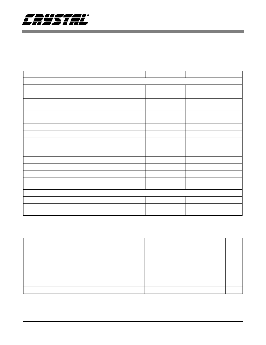
Parameter*
Symbol
Min
Typ
Max
Units
Dynamic Performance
DAC Resolution
16
-
-
Bits
DAC Differential Nonlinearity
DNL
-
-
±
0.9
LSB
Total Harmonic Distortion
AOUTL, AOUTR
(Note 1)
AOUTM
THD
-
0.01
0.02
0.015
0.03
%
Instantaneous Dynamic Range
AOUTL, AOUTR
(Note 1)
(DAC not muted, A weighted)
AOUTM
IDR
85
80
90
85
-
dB
Interchannel Isolation
(Note 1)
-
85
-
dB
Interchannel Gain Mismatch
-
-
0.2
dB
Frequency Response
-3.0
-
+0.2
dB
Full Scale output Voltage
AOUTL, AOUTR
(Note 1)
AOUTM
2.66
2.7
2.88
3.0
3.2
3.3
Vpp
Gain Drift
-
100
-
ppm/∞C
Deviation from Linear Phase
-
-
5
Deg
Out of Band Energy
(Fs/2 to 2Fs)
-
-60
-
dB
Analog Output Load
Resistance:
Capacitance:
8
-
-
-
-
100
k
pF
Power Supply
Power Supply Rejection
(1 kHz)
-
40
-
dB
Power Supply Consumption
VA+
VD+
-
-
20
100
40
140
mA
mA
Parameter
Symbol
Min
Typ
Max
Units
Passband (to -3 dB corner)
(Fs is conversion freq.).
0
-
0.476Fs
Hz
Passband
Ripple. -
-
±
0.1
dB
Transition Band.
0.442Fs
-
0.567Fs
Hz
Stop Band.
0.567Fs
-
-
Hz
Stop Band Rejection.
50
-
-
dB
Stop Band Rejection with Ext. 2Fs RC filter.
57
-
-
dB
Group
Delay. -
12/Fs
-
s

CS4922
5
ABSOLUTE MAXIMUM RATINGS
(AGND, DGND = 0V, all voltages with respect to ground.)
WARNING: Operation at or beyond these limits may result in permanent damage to the device.
Normal operation is not guaranteed at these extremes.
RECOMMENDED OPERATING CONDITIONS
(AGND, DGND = 0V; all voltages with respect
to ground.)
DIGITAL CHARACTERISTICS
(T
A
= 25
∞
C; VA+, VD+ = 5V
±
10%; measurements performed under
static conditions.)
Notes: 2. Not Valid for pin numbers 9, 12, 13, and 30 which are configured with on-chip pull-down resistors. Not
valid for pin number 29 which is a static input signal and should be tied to either VD+ or DGND.
Parameter
Symbol
Min
Max
Units
DC Power Supplies:
Positive Digital
Positive Analog
| | VA+ | - | VD+ | |
VD+
VA+
-0.3
-0.3
-
6.0
6.0
0.4
V
V
V
Input Current, Any Pin Except Supplies
I
in
-
±
10
mA
Digital Input Voltage
V
IND
-0.3
(VD+) + 0.4
V
Ambient Operating Temperature (power applied)
T
Amax
-55
125
∞C
Storage Temperature
T
stg
-65
150
∞C
Parameter
Symbol
Min
Typ
Max
Units
DC Power Supplies:
Positive Digital
Positive Analog
| | VA+ | - | VD+ | |
VD+
VA+
4.50
4.50
-
5.0
5.0
-
5.50
5.50
0.4
V
V
V
Ambient Operating Temperature
T
A
0
-
70
∞C
Parameter
Symbol
Min
Typ
Max
Units
High-Level Input Voltage
V
IH
TBD
2.25
-
V
Low-Level Input Voltage
V
IL
-
-
0.8
V
High-Level Output Voltage at I
o
= -2.0 mA
V
OH
VD x 0.9
-
-
V
Low-Level Output Voltage at I
o
= 2.0 mA
V
OL
-
-
VD x 0.1
V
Input Leakage Current
(Note 2)
I
in
-
-
1.0
µ
A