 | –≠–ª–µ–∫—Ç—Ä–æ–Ω–Ω—ã–π –∫–æ–º–ø–æ–Ω–µ–Ω—Ç: CS61600-I | –°–∫–∞—á–∞—Ç—å:  PDF PDF  ZIP ZIP |
Document Outline
- CS61600: PCM Jitter Attenuator
- Features
- General Description
- Characteristics & Specifications
- ABSOLUTE MAXIMUM RATINGS
- RECOMMENDED OPERATING CONDITIONS
- DIGITAL CHARACTERISTICS
- DIGITAL CHARACTERISTICS
- SWITCHING CHARACTERISTICS
- Figure 1. Signal Rise and Fall Characteristics
- Figure 2. Clock Signal Quality
- Figure 3. Switching Characteristics
- Figure 4. Input Jitter Tolerance
- Figure 5. Jitter Attenuation Characteristic
- CIRCUIT DESCRIPTION
- Jitter Attenuation
- Figure 6. Jitter Attenuation Characteristics
- Using the CS61600 in a Slave Configuration
- Oscillator and Crystal
- FIFO Overflow/Underflow
- FIFO Reset
- Power-Up Reset
- Schematic & Layout Review Service
- PIN DESCRIPTIONS
- Pin-out drawing
- Power Supplies
- Oscillator
- Control
- Inputs
- Outputs
- APPLICATIONS
- Figure A1. Typical Application Circuit
- Selecting an Oscillator Crystal
- General Applications
- Master/Slave Configuration
- Figure A2. Master / Slave configuration
- Maintaining Clock
- Jitter Attenuation at Different Clock Rates
- Figure A3. Maintaining Clock Integrity
- Figure A4. Low Clock Frequency Jitter Attenuation
- Package Dimensions
- 14 PIN PLASTIC (PDIP) PACKAGE DRAWING

Features
∑
∑
Unique Clock-Tracking Circuitry Filters
50 Hz or Higher Frequency Jitter for
T1 and PCM-30 Applications
∑
∑
Minimal External Components Required
∑
∑
14 Pin DIP
∑
∑
Single 5 Volt Supply
∑
∑
3 Micron CMOS for High Reliability
and Low Power Dissipation: 50 mW
Typical at 25
∞
C
General Description
The CS61600 from Crystal Semiconductor accepts T1
(1.544 Mb/s) or CCITT standard (2.048 Mb/s) data and
clock inputs, and tolerates at least 7 (and up to 14) unit
intervals, peak-to-peak, of jitter. Before outputting data
and clock, jitter is attenuated using an internal clock-
tracking variable oscillator and a 16 bit FIFO elastic
store.
The jitter attenuation function can be determined by
appropriate specification of the external crystal.
The CS61600 is transparent to data format, and is in-
tended for application in carrier systems, switching
systems, Local Area Network gateways and multiplex-
ers.
ORDERING INFORMATION
CS61600-IP1
-
14 Pin Plastic DIP; T1 and 2.048 MHz
APR '90
DS9F3
1
Crystal Semiconductor Corporation
P.O. Box 17847, Austin, TX 78760
(512) 445-7222 FAX: (512) 445-7581
PCM Jitter Attenuator
Semiconductor Corporation
CS61600
16-BIT FIFO
VARIABLE OSCILLATOR
4
13
8
XTALIN
CLKIN
DIN
FIFO CONTROL
2
3
1
FIFORST
OVR
RESET
HALF FULL
DETECT
OSCOUT
5
XTALOUT
11
10
6
CLKOUT
ARE
14
7
GND
V+
12
ARC
9
DOUT
˜
4
Copyright
©
Crystal Semicondutor Corporation 1994
(All Rights Reserved)
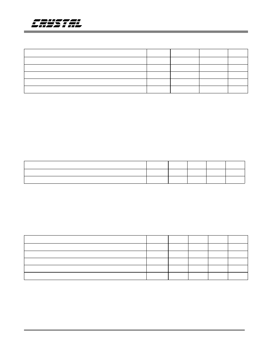
ABSOLUTE MAXIMUM RATINGS
Parameter
Symbol
Min
Max
Units
DC Supply
(V+)-GND
-0.3
7.0
V
Input Voltage
V
in
GND - 0.3
(V+) + 0.3
V
Input Current, Any Pin
(Note 1)
I
in
-10
10
mA
Ambient Operating Temperature
T
A
-40
85
∞C
Storage Temperature
T
stg
-65
150
∞C
Note:
1. Transient currents of up to 100 mA will not cause SCR latch-up.
WARNING: Operation at or beyond these limits may result in permanent damage to the device.
Normal operation is not guaranteed at these extremes.
RECOMMENDED OPERATING CONDITIONS
Parameter
Symbol
Min
Typ
Max
Units
DC Supply
(V+)-GND
4.5
5.0
5.5
V
Ambient Operating Temperature
T
A
-40
25
85
∞C
DIGITAL CHARACTERISTICS
(T
A
= -40∞ to 85∞ C; V+ = 5V
±
10%; GND = 0V)
Parameter
Symbol
Min
Typ
Max
Units
High-Level Input Voltage
V
IH
2.0
-
-
V
Low-Level Input Voltage
V
IL
-
-
0.8
V
High-Level Output Voltage
(Notes 2 and 3)
V
OH
2.4
-
-
V
Low-Level Output Voltage
(Notes 2 and 4)
V
OL
-
-
0.4
V
Input Leakage Current
I
in
-
-
±
10.0
µ
A
Notes:
2. Outputs will drive CMOS logic levels into a CMOS load.
3. I
out
= -40
µ
A
4. I
out
= 1.6 mA
Specifications subject to change without notice.
CS61600
2
DS9F3

DIGITAL CHARACTERISTICS
(T
A
= -40∞ to 85∞ C; V+ = 5V
±
10%; GND = 0V)
Parameter
Symbol
Min
Typ
Max
Units
Power Dissipation
P
D
-
50
85
mW
Input Jitter Tolerance
7
-
14*
U.I.
* Depends on accuracy of crystal with respect to CLKIN frequency. See
Applications
section.
SWITCHING CHARACTERISTICS
(T
A
= -40∞ to 85∞ C; V+ = 5V
±
10%; GND = 0V;
Inputs: Logic 0 = 0V, Logic 1 = V+)
Parameter
Symbol
Min
Typ
Max
Units
Crystal Frequency
T1
CCITT
(Note 5)
f
c
-
-
6.176000
8.192000
-
-
MHz
CLKIN Frequency
T1
CCITT
(Note 6)
f
in
-
-
1.544
2.048
-
-
MHz
CLKOUT Frequency
T1
CCITT
(Note 6)
f
out
-
-
1.544
2.048
-
-
MHz
Clock Pulse Width
T1
CCITT
(Note 7)
t
pwh
t
pwl
-
-
324
324
-
-
ns
t
pwh
t
pwl
-
-
244
244
-
-
ns
Acceptable CLKIN range
(Note 8)
-
±
130
-
ppm
Duty Cycle
(Note 9)
-
50
-
%
Rise Time, All Digital Outputs
(Note 10)
t
r
-
36
100
ns
Fall Time, All Digital Outputs
(Note 10)
t
f
-
17
100
ns
DIN to CLKIN Falling Setup Time
t
su
30
-
-
ns
CLKIN Falling to DIN Hold Time
t
h
50
-
-
ns
CLKOUT Falling to DOUT Propogation Delay
t
phl
-
-
200
ns
Note:
5. Crystal should have sufficient pull range when in the oscillator circuit, to meet the system's frequency
tolerance requirement over the operating temperature range. See
Applications
section for more
information on crystals.
6. Although CLKIN and CLKOUT will vary in instantaneous frequency (jitter) over time, CLKOUT
will have the same average frequency as CLKIN.
7. The sum of the pulse widths must always meet the frequency specifications.
8. Crystal must have at least
±
130ppm pull range over operating temperature range.
9. Duty cycle is (t
PWH
/ (t
PWH
+ t
PWL
)) x 100%.
10. At C
L
= 50pF.
CS61600
DS9F3
3

CLKIN, CLKOUT
t
pwh
t
pwl
Figure 2. Clock Signal Quality
CLKIN
DIN
CLKOUT
DOUT
t
su
t
h
t
phl
Figure 3. Switching Characteristics
Any Digital Output
t r
t f
10%
10%
90%
90%
Figure 1. Signal Rise and Fall Characteristics
CS61600
4
DS9F3

0
-10
-20
-30
-40
JITTER
GAIN
(dB)
10
100
1k
10k
BELL SYSTEM
PUB 43802
SPECIFICATION
CS61600
PERFORMANCE
Input of five
unit intervals
of jitter at all
frequencies.
JITTER FREQUENCY (Hz)
20 dB/
decade
Figure 5. Jitter Attenuation Characteristic
7.0
5.0
0.1
10.0
500
8.0k
AT&T
43802
SPECIFICATION
CS61600 PERFORMANCE
PEAK-TO-PEAK
(SINUSOIDAL)
JITTER
AMPLITUDE
IN UNIT
INTERVALS
JITTER FREQUENCY (Hz)
10.0
1.0
0.2
CCITT
G.823
SPECIFICATION
100.0
1.0k
10.0k
18k
2.4k
20
1.5
Figure 4. Input Jitter Tolerance
CS61600
DS9F3
5
CIRCUIT DESCRIPTION
Jitter Attenuation
The CS61600 will tolerate and attenuate at least
seven unit intervals of jitter from clock and data
signals of 1.544 MHz and 2.048 MHz. An
external clock divide circuit can be added for
jitter attenuation for lower frequency signals.
Jitter attenuation is accomplished by means of a
FIFO and a variable oscillator. The frequency of
the oscillator is controlled by logic in the
CS61600 to be the same as the average of the
input clock signal, CLKIN. Signal jitter is ab-
sorbed in the FIFO.
The FIFO's write pointer is controlled by the
CLKIN signal. Data present on DIN is written
into the memory location selected by the write
pointer. The CLKOUT signal corresponds to the
FIFO's read pointer and is controlled by the
crystal oscillator. Internal logic determines the
relationship of the read pointer and the write
pointer, and adjusts the speed of the oscillator.
For example, if the CLKIN signal is at a higher
frequency than the CLKOUT signal, the write
pointer will start to catch up with the read
pointer. When this situation is detected, the ca-
pacitive loading the device presents to the crystal
is reduced, resulting in an increase in oscillator
frequency and read pointer (CLKOUT) fre-
quency. The oscillator frequency is periodically
updated and adjusted to maintain the FIFO at
half full. High frequency variations in the phase
of the CLKIN signal (jitter) are absorbed in the
FIFO.
There are some advantages to this method of
jitter attenuation. The device can tolerate large
amplitude jitter at high frequencies. The device
can track slow changes of the input clock fre-
quency (wander) and tolerate input frequencies
ranging over a specified frequency tolerance.
A by product of this method of jitter attenuation
is that the greater the input jitter, the greater the
jitter attenuation, and the lower the frequency at
which the device starts to attenuate jitter.
Conversely, low amplitude jitter receives little
attenuation. This performance characteristic is
shown graphically in Figure 6.
Using the CS61600 in a Slave Configuration
It is possible to use an externally generated clock
signal to clock data out of the CS61600. When
an external clock is used, a crystal is not neces-
sary. The external clock is input to the Alternate
Read Clock input, ARC (pin 12). Holding the
Alternate Read Enable pin, ARE (pin 6), high di-
rects the CS61600 to clock data out of the FIFO
at the rate determined by ARC. Unless the clock
signal on ARC is at exactly the same average
frequency as the clock signal on CLKIN, the
CS61600 will be prone to underflow or overflow,
and data will be lost. See the Applications sec-
tion of this data sheet for more information on
the use of an alternate clock.
Oscillator and Crystal
The CS61600 requires an external 6.176000
MHz (8.192000 MHz for CCITT) crystal be
connected to pins XTALOUT and XTALIN. The
oscillator circuit divides the crystal frequency by
four, and switches various capacitive loads to
provide a clock that swings in five steps from at
le ast 1.544 MHz - 130 ppm to at least
1.544 MHz + 130 ppm (2.048 MHz - 50 ppm to
JITTER
GAIN
(dB)
0
-10
-20
-30
-40
10
100
1k
10k (Hz)
dB
5
...
UNIT INTERVALS
OF INPUT JITTER
3
1
Measurement made at 1.544 MHz
with 6.176 MHz ±200 ppm crystal.
Figure 6. Jitter Attenuation Characteristics
CS61600
6
DS9F3

2.048 MHz + 50 ppm for CCITT). The crystal
oscillator must be able to reach these signal fre-
quency tolerances over the system's operating
temperature range. The oscillator adjusts to and
holds the average frequency of the signal input
to CLKIN.
Some applications specify a narrower frequency
tolerance. In these cases, it is possible to im-
prove jitter attenuation performance by specify-
ing a crystal with less pull range. A narrow pull
range crystal has the effect of shifting the curves
shown in Figure 6 to the left. Care must be taken
to ensure that the crystal/oscillator will reach the
signal's frequency extremes over the operating
temperature range of the system. More informa-
tion on specifying and testing crystals is pro-
vided in the Applications section at the back of
this data sheet.
FIFO Overflow/Underflow
Because the oscillator clock, which is used to
empty the FIFO, has a wider frequency range
than the standard T1 input signal, the FIFO
should never underflow or overflow. However, if
underflow or overflow occurs, the buffer
overflow/underflow flag, OVR (pin 3), goes
high. A RESET (pin 1) resets the overflow flag.
If an overflow occurs, the 16 bits of data in the
FIFO are lost. An underflow condition causes the
next 16 bits read from the FIFO to be invalid. In
either case, the CS61600 will immediately
attempt to relock on to the clock signal. Holding
RESET low disables the overflow flag, OVR.
FIFO Reset
Taking the FIFORST pin low causes most of the
subcircuits of the CS61600 to go into a reset
state. These circuits will remain in a reset
condition until FIFORST is returned to a logic 1
state. However, the outputs of the CS61600 are
undefined if FIFORST is held low for more
than 500 ms. The FIFO reset function will set
the FIFO write and read pointers to the first and
eighth locations respectively. The oscillator will
continue to run and CLKOUT will be held low.
Power-Up Reset
Upon power up, the CS61600 goes through an
i n i t i al i z at i o n p r o c ed u r e w h i ch r eq u i r es
approximately 3 ms. During this initialization
procedure, OVR is held high. After initialization
is complete, OVR goes low. When the clock
signal is input to CLKIN, the CS61600 will
immediately try to lock onto the clock signal on
CLKIN. At this point, the FIFO may overflow,
and the RESET pin should be toggled to clear
the overflow/underflow flag, OVR.
Schematic & Layout Review Service
Confirm Optimum
Schematic & Layout
Before Building Your Board.
For Our Free Review Service
Call Applications Engineering.
C a l l : ( 5 1 2 ) 4 4 5 - 7 2 2 2
CS61600
DS9F3
7

PIN DESCRIPTIONS
Power Supplies
V+ - Positive Power Supply, PIN 14.
Typically +5V volts.
GND - Ground, PIN 7.
Ground reference.
Oscillator
XTALIN, XTALOUT - Crystal Input 1, 2; PINS 4, 5.
6.176 MHz or 8.192 MHz crystal inputs. A 200 kohm resistor should be connected across these
pins. There is no need for external capacitors. The crystal should be connected to XTALIN and
XTALOUT with minimal length traces on the pc board.
Control
RESET - Reset, PIN 1.
When RESET is taken low, the OVR signal is reset.
FIFORST - FIFO Reset, PIN 2.
Taking FIFORST low resets the read and write pointers of the FIFO. Resetting the pointers will
cause some data loss. When FIFORST is low, the OSCOUT output is disabled.
ARE - Alternate Read Enable, PIN 6.
For normal operation, ARE is held at logic 0. In this configuration the oscillator controls the
read pointer of the FIFO. When ARE is at logic 1, the read pointer of the FIFO will be
controlled by the clock signal on pin 12, ARC.
1
2
3
4
5
6
7
14
13
12
11
10
9
8
RESET
RESET
V+
POWER SUPPLY
FIFO RESET
FIFORST
DIN
DATA INPUT
BUFFER OVERFLOW/UNDERFLOW
OVR
ARC
ALTERNATE READ CLOCK
CRYSTAL OUTPUT
XTALIN
OSCOUT
OSCILLATOR OUTPUT
CRYSTAL INPUT
XTALOUT
CLKOUT
OUTPUT CLOCK
ALTERNATE READ ENABLE
ARE
DOUT
DATA OUTPUT
GROUND
GND
CLKIN
INPUT CLOCK
CS61600
8
DS9F3

Inputs
CLKIN - Clock Input, PIN 8.
Clock for the data input. This clock contains the jitter to be removed.
DIN - Data Input, PIN 13.
Input data is sampled on the falling edge of CLKIN.
ARC - Alternate Read Clock, PIN 12.
When ARE, Pin 6, is at logic 1, a clock signal on ARC will control the FIFO's read pointer.
CLKOUT, pin 10, will be at the same frequency and phase as ARC. Setting ARE to logic 0
results in the device using its oscillator to generate CLKOUT.
Outputs
OVR - Buffer Overflow/Underflow, PIN 3.
Goes high if the FIFO overflows or underflows, and is cleared by RESET.
DOUT - Data Output, PIN 9.
Output data with jitter attenuated. DOUT is stable and valid on the rising edge of CLKOUT.
CLKOUT - Output Clock, PIN 10.
Jitter reduced clock output corresponding to the data on DOUT.
OSCOUT - Oscillator Output, Pin 11.
Output of on-chip oscillator, divided by four. This pin should be left floating for normal
operation.
CS61600
DS9F3
9

APPLICATIONS
Selecting an Oscillator Crystal
Specific crystal parameters are required for
proper operation of the CS61600. It is recom-
me nd ed that th e Crystal Semi conducto r
CXT6176 crystal be used for T1 applications
and the CXT8192 crystal be used for PCM-30
applications.
General Applications
The CS61600 will tolerate and attenuate at least
seven unit intervals of jitter over the specified
range of input clock and oscillator frequencies. If
the oscillator crystal is chosen so that the center
frequency of its pull range is close to the input
frequency, CLKIN, the CS61600 will tolerate
more jitter; up to 14 unit intervals will be toler-
ated under optimal conditions.
Consider the case where the average clock
frequency at CLKIN approaches the slow end of
the range, 1.544 MHz - 130 ppm. In this case,
the oscillator will be near the bottom of its
pull range, restricting its ability to achieve
frequencies well below the CLKIN frequency.
The result is that the read pointer of the FIFO
will begin to catch up to the write pointer. If
enough jitter is introduced, the read pointer will
overtake the write pointer resulting in an error
(i.e. the device will try to read out data before it
is written in). A similar situation occurs when
the CLKIN signal approaches the fast end of its
range, 1.544 MHz + 130 ppm.
Taking care in selecting the proper crystal can
result in improved jitter tolerance without de-
grading the performance of the CS61600. If the
center frequency of the oscillator is precisely
four times the CLKIN frequency, and the crystal
has at least the specified pull range, the CS61600
will tolerate 14 unit intervals of jitter. In this
case, the read and write pointers of the FIFO
will maintain optimal separation when the
signal is jitter free, allowing the device to toler-
ate maximum jitter input.
Master/Slave Configuration
Some T1 applications require separate repre-
sentations of the positive and negative going
pulses for an AMI signal. Two CS61600s can be
used to remove jitter from a set of signals con-
sisting of POS, NEG and CLK. Figure A2 shows
the master/slave configuration.
This configuration requires one crystal (on the
master). The CLKOUT signal from the master
controls the FIFO read pointer of the slave
CS61600. Setting ARE, pin 6, of the slave to
logic 1 directs the device to use the clock input
to ARC, pin 12, to control the FIFO read pointer.
For this configuration to function properly, the
positions of the FIFO read and write pointers in
both devices must correspond. The FIFO pointer
reset, FIFORST, of both devices must be tied to-
RESET
FIFORST
OVR
XTALIN
ARE
GND
V+
DIN
ARC
OSCOUT
CLKOUT
DOUT
CLKIN
14
13
12
11
10
9
8
1
2
3
4
5
6
7
JITTERED CLOCK INPUT
JITTER FREE CLOCK
JITTER FREE DATA
JITTERED DATA INPUT
+5V
V+
RESET
V+
10k
10k
XTALOUT
200k
6.176 MHz
Figure A1. Typical Application Circuit
CS61600
10
DS9F3
gether. After the power supplies have stabilized,
and the clock has been input at CLKIN, FI-
FORST should be momentarily pulled low to re-
set the pointers of both devices. The overflow
flags should then be reset by momentarily pull-
ing RESET, pin 1, low.
Additional slaves may be added. The ARC input
may be derived from either the CLKOUT pin on
the master, or the CLKOUT pin on a preceding
slave. When using the master's CLKOUT pin,
the fan out must be considered. Attaching several
inputs to the CLKOUT pin increases the load
that the output must drive. The added capaci-
tance will reduce the switching speed of the out-
put driver. Similarly, a configuration which uses
the CLKOUT signal of each CS61600 to drive
the subsequent CS61600 will induce some
propagation delay. These potential timing prob-
lems should be considered when cascading
CS61600s.
Maintaining Clock
Many applications require that the clock signal
from CLKOUT be maintained within some
specified range of frequencies when the clock
signal on CLKIN (often generated from a recov-
ered T1 signal clock) goes away. Figure A3
shows one method for maintaining the CLKOUT
signal. The reference clock is a locally generated
clock whose frequency lies within the tolerance
of the applicable specifications which govern the
system's design. When the CLKIN signal goes
away, the multiplexor should switch in the refer-
ence clock. Since this clock goes through the jit-
ter attenuator, phase and frequency integrity at
CLKOUT is maintained.
Jitter Attenuation at Different Clock Rates
The CS61600 can be used to attenuate jitter at
frequencies below 2.048 MHz. For signal fre-
quencies above about 900 kHz, selection of the
appropriate crystal will suffice. For jitter attenu-
10k
V+
1
2
3
4
5
6
7
NC
NC
NC
NC
14
13
12
11
10
9
8
V+
V+
DIN
1
DIN
2
CLKIN
DOUT
2
CLKOUT
10k
V+
CS61600
MASTER
ARC
ARE
DOUT
1
OVR
RESET
OVR
RESET
200k
multiple
slaves
may be
added
NC
OVR
OVR
Q
S
R
D
Q
CLKIN
V+
10k
V+
1
2
3
4
5
6
7
14
13
12
11
10
9
8
CS61600
SLAVE
10k
V+
FIFO
POINTER
RESET
Figure A2. Master / Slave configuration
LOCALLY
GENERATED
REFERENCE
CLOCK
RECOVERED
CLOCK
LOSS OF
CLOCK
DETECTOR
MULTIPLEXER
CS61600
CLKIN
pin 8
1.544 MHz
1.544 MHz
CLKOUT
pin 10
Figure A3. Maintaining Clock Integrity
CS61600
DS9F3
11

ation of lower frequency signals, an external di-
vider is required. Figure A4 shows how the
CS61600 can be configured for low frequency
jitter attenuation.
Frequency tolerance of the input signal is still
based on the pull range of the crystal in ppm.
For example, a 64 kbps jitter attenuator which
uses an external divide by 32, and a 8.192 MHz
crystal with
±
200 ppm pull range will have
+ 200 ppm tolerance at 64 kbps or + 12.8 Hz.
1
2
3
4
5
6
7
14
13
12
11
10
9
8
DIN
1
CLKIN
CLKOUT
10k
V+
CS61600
DOUT
1
200k
RESET
10k
FIFORST
+5V
4.5 MHz to 8.2 MHz
10k
V+
ARE
DIVIDER
ARC
OSCOUT
Figure A4. Low Clock Frequency Jitter Attenuation
CS61600
12
DS9F3
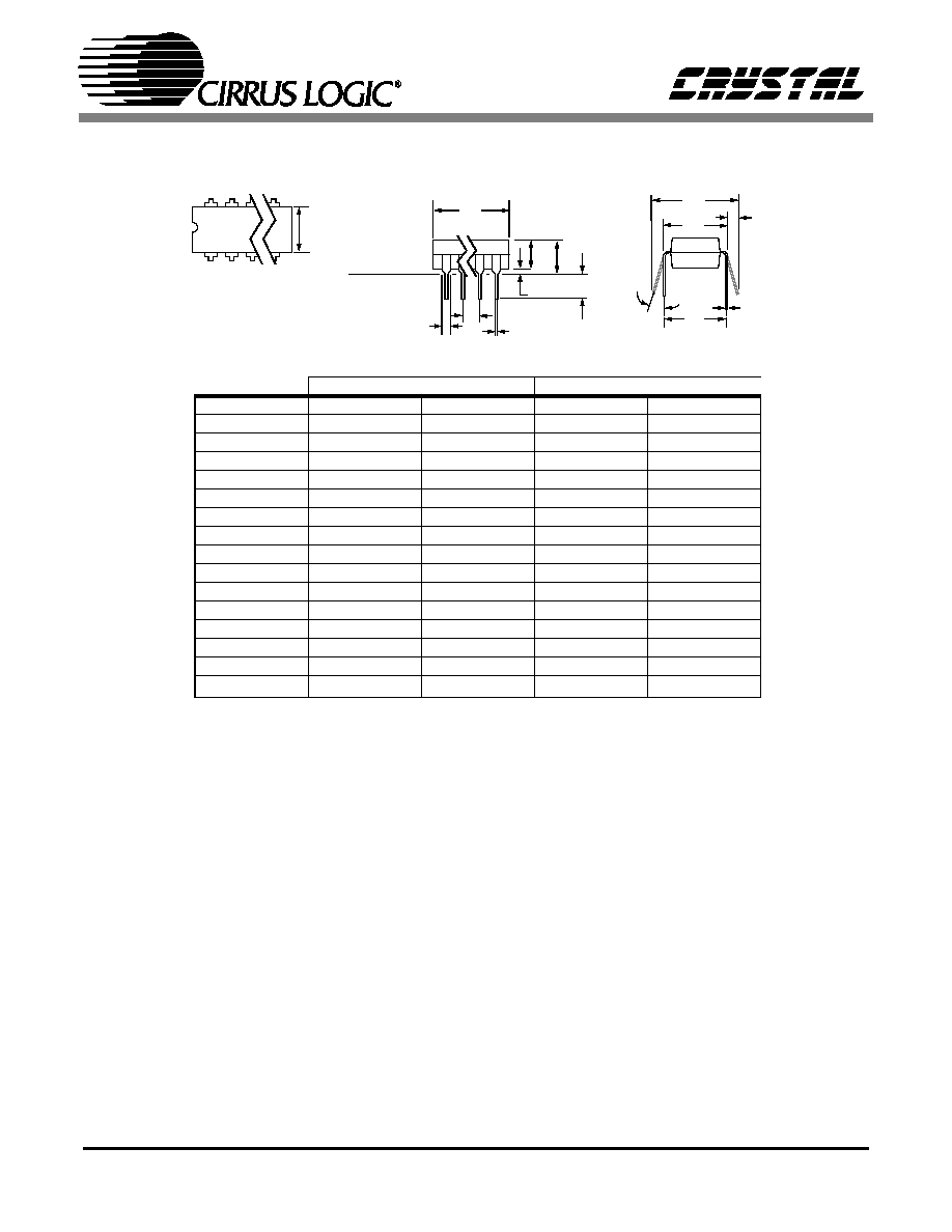
8/24/99 : CIRRUS LOGIC --- CRYSTAL SEMICONDUCTOR : 14 PIN PLASTIC (PDIP) PACKAGE DRAWING
INCHES
MILLIMETERS
DIM
MIN
MAX
MIN
MAX
A 0.000
0.210
0.00
5.33
A1
0.015
0.025
0.38
0.64
A2
0.115
0.195
2.92
4.95
b
0.014
0.022
0.36
0.56
b1
0.045
0.070
1.14
1.78
c
0.008
0.014
0.20
0.36
D
0.735
0.775
18.67
19.69
E
0.300
0.325
7.62
8.26
E1
0.240
0.280
6.10
7.11
e
0.090
0.110
2.29
2.79
eA
0.280
0.320
7.11
8.13
eB
0.300
0.430
7.62
10.92
eC
0.000
0.060
0.00
1.52
L
0.115
0.150
2.92
3.81
0∞
15∞
0∞
15∞
14 PIN PLASTIC (PDIP) PACKAGE DRAWING
E1
D
SEATING
PLANE
b1
e
b
A
L
A1
TOP VIEW
BOTTOM VIEW
SIDE VIEW
1
eA
c
A2
E
eC
eB

Contacting Cirrus Logic Support
For a complete listing of Direct Sales, Distributor, and Sales Representative contacts, visit the Cirrus Logic web site at:
http://www.cirrus.com/corporate/contacts/
Preliminary product information describes products which are in production, but for which full characterization data is not yet available. Advance product infor-
mation describes products which are in development and subject to development changes. Cirrus Logic, Inc. has made best efforts to ensure that the information
contained in this document is accurate and reliable. However, the information is subject to change without notice and is provided "AS IS" without warranty of
any kind (express or implied). No responsibility is assumed by Cirrus Logic, Inc. for the use of this information, nor for infringements of patents or other rights
of third parties. This document is the property of Cirrus Logic, Inc. and implies no license under patents, copyrights, trademarks, or trade secrets. No part of
this publication may be copied, reproduced, stored in a retrieval system, or transmitted, in any form or by any means (electronic, mechanical, photographic, or
otherwise) without the prior written consent of Cirrus Logic, Inc. Items from any Cirrus Logic website or disk may be printed for use by the user. However, no
part of the printout or electronic files may be copied, reproduced, stored in a retrieval system, or transmitted, in any form or by any means (electronic, mechanical,
photographic, or otherwise) without the prior written consent of Cirrus Logic, Inc.Furthermore, no part of this publication may be used as a basis for manufacture
or sale of any items without the prior written consent of Cirrus Logic, Inc. The names of products of Cirrus Logic, Inc. or other vendors and suppliers appearing
in this document may be trademarks or service marks of their respective owners which may be registered in some jurisdictions. A list of Cirrus Logic, Inc. trade-
marks and service marks can be found at http://www.cirrus.com.