| –≠–ª–µ–∫—Ç—Ä–æ–Ω–Ω—ã–π –∫–æ–º–ø–æ–Ω–µ–Ω—Ç: CS61881 | –°–∫–∞—á–∞—Ç—å:  PDF PDF  ZIP ZIP |
Document Outline
- CS61881
- Features
- Description
- Table of Contents
- List of Figures
- List of Tables
- Contacting Cirrus Logic Support
- 1. CHARACTERISTICS AND SPECIFICATIONS
- ABSOLUTE MAXIMUM RATINGS
- RECOMMENDED OPERATING CONDITIONS
- DIGITAL CHARACTERISTICS
- ANALOG SPECIFICATIONS
- SWITCHING CHARACTERISTICS
- Figure 1. Signal Rise and Fall Characteristics
- Figure 2. Recovered Clock and Data Switching Characteristics
- Figure 3. Transmit Clock and Data Switching Characteristics
- 2. THEORY OF OPERATION
- 2.1 Transmitter
- Figure 4. Mask of the Pulse at the 2048 kbps Interface
- 2.2 Receiver
- 2.3 Loss-of-Signal Detector
- 2.4 Loopback
- 2.4.1 Local Loopback
- 2.4.2 Remote Loopback
- 2.5 5V Logic Support
- 2.6 JTAG Support
- 2.6.1 TAP Controller
- Figure 5. Test Access Port Architecture
- Figure 6. TAP Controller State Diagram
- 2.6.2 Test-Logic-Reset
- 2.6.3 Run-Test-Idle
- 2.6.4 Select-DR-Scan
- 2.6.5 Capture-DR
- 2.6.6 Shift-DR
- 2.6.7 Exit1-DR
- 2.6.8 Pause-DR
- 2.6.9 Exit2-DR
- 2.6.10 Update-DR
- 2.6.11 Select-IR-Scan
- 2.6.12 Capture-IR
- 2.6.13 Shift-IR
- 2.6.14 Exit1-IR
- 2.6.15 Pause-IR
- 2.6.16 Exit2-IR
- 2.6.17 Update-IR
- 2.7 JTAG Instruction Register (IR)
- Table 1. JTAG Instructions
- 2.7.1 EXTEST
- 2.7.2 SAMPLE/PRELOAD
- 2.7.3 IDCODE
- 2.7.4 BYPASS
- 2.8 Boundary Scan Register (BSR)
- Table 2. Boundary Scan Register
- 3. PIN DESCRIPTION
- 3.1 Pinout - 144-Pin LQFP
- Figure 7. 144-Pin LQFP Pin Description Drawing
- 3.2 Pinout - 160-Pin FBGA
- Figure 8. 160-Pin FBGA Pin Description Drawing
- 3.3 Pin Descriptions
- Power Supplies
- Control
- Status
- RX/TX Data I/O
- JTAG Test Interface
- Miscellaneous
- No Connects
- 4. PACKAGE DIMENSIONS
- 144L TQFP PACKAGE DRAWING
- 160-BALL FBGA (2 LAYER) PACKAGE DRAWING
- 5. APPLICATIONS
- Figure 9. Internal RX Impedance Matching
- Figure 10. External RX Impedance Matching

Preliminary Product Information
This document contains information for a new product.
Cirrus Logic reserves the right to modify this product without notice.
1
Copyright
Cirrus Logic, Inc. 2000
(All Rights Reserved)
P.O. Box 17847, Austin, Texas 78760
(512) 445 7222 FAX: (512) 445 7581
http://www.cirrus.com
CS61881
Octal E1 Analog Front End
Features
s
Octal E1 Line Interface Unit Compliant with G.703
s
Very Low Power <100mW per Channel
s
Single Supply 3.3 V Operation, 5 V Tolerant I/O
s
No External Component Changes for 120
/75
Operation
s
Analog LOS Detection per ITU G.775
s
Transmitter Short Circuit Current Limiter (<50mA)
s
TX Drivers with Fast Tristate and Power Down
s
Transmit Return Loss Exceeds ETS 300 166
s
JTAG Boundary Scan compliant to IEEE 1149.1
s
144 Pin LQFP or 160 BGA Package
ORDERING INFORMATION
CS61881-IQ
144-pin LQFP
CS61881-IB
160-pin BGA
Description
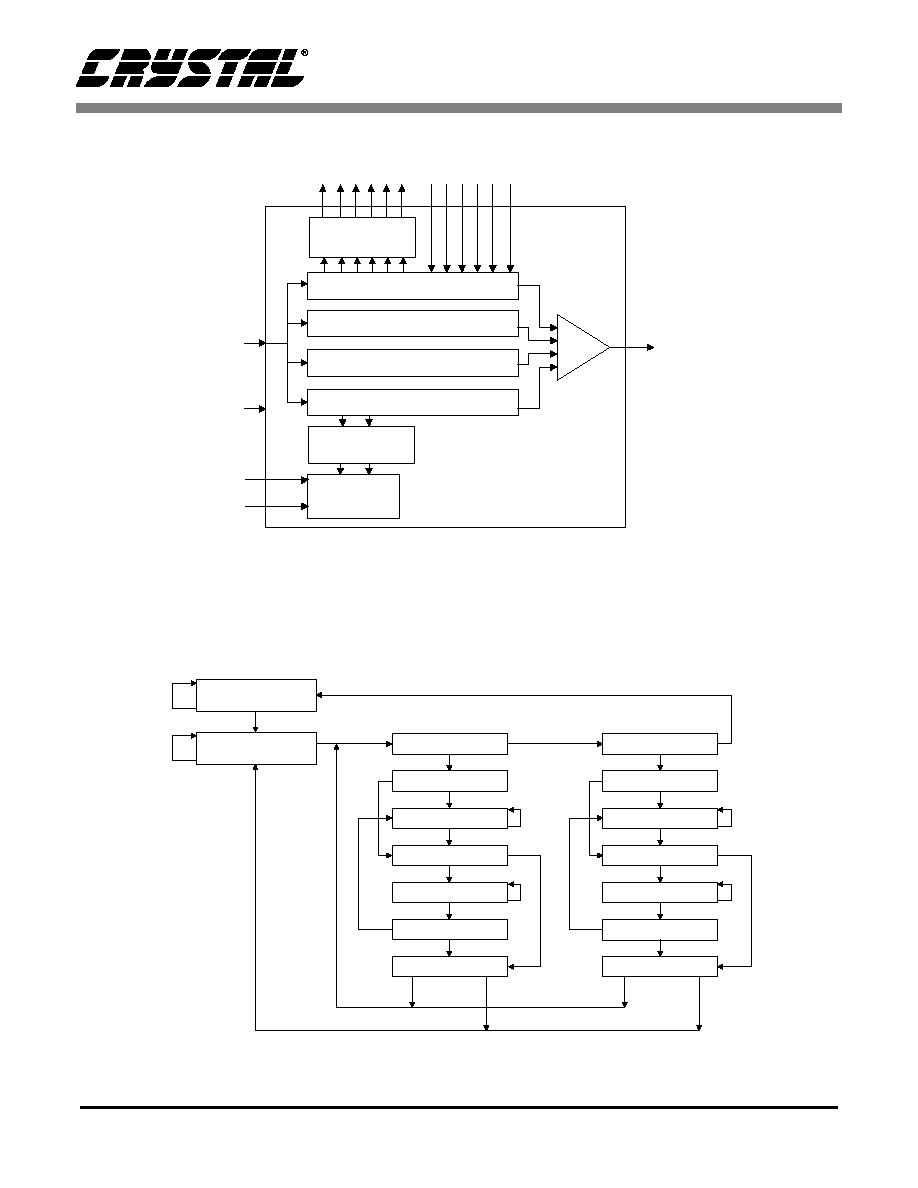
The CS61881contains eight analog front ends that each
provide the line interface for E1 transmission systems.
The device contains eight receivers and transmitters
supporting a 2.048 Mbps data rate compliant to ITU
G.703. This device is commonly used with external cir-
cuitry that supplies data encoding/decoding, clock
recovery, and jitter attenuation.
The CS61881 makes use of ultra low power matched im-
pedance transmitters to reduce power beyond that
achieved by traditional driver designs. By achieving a
more precise line match, this technique also provides su-
perior return loss characteristics, exceeding ETS 300
166. The internal line matching circuitry reduces the ex-
ternal component count and eliminates the need to
change components to support both 75
and 120
lines. All transmitters have controls for independent pow-
er down and tristate.
The receiver has a high noise margin, providing reliable
data recovery even with cable attenuation of over 12 dB.
It has an impedance matched front end, eliminating the
need to change components to support both 75
and
120
line impedances. The receiver also incorporates
LOS detection compliant to the most recent
specifications.
A five wire JTAG interface is also provided for improved
diagnostics and reduced manufacturing cost.
Driver
Peak
Detect
RPOS
RNEG
TPOS
TNEG
TCLK
LOS
Slicer
G.775
LOS
Pulse
Shaper
1
2
8
RTIP
RRING
TTIP
TRING
Lo
c
a
l
Lo
op
ba
c
k
XOR
RCLK
Re
m
o
t
e
Lo
op
ba
c
k
JTAG
Serial
Port
JTAG Interface
APR `00
DS451PP3

CS61881
2
DS451PP3
TABLE OF CONTENTS
1. CHARACTERISTICS AND SPECIFICATIONS ........................................................................ 4
ABSOLUTE MAXIMUM RATINGS ........................................................................................... 4
RECOMMENDED OPERATING CONDITIONS ....................................................................... 4
DIGITAL CHARACTERISTICS ................................................................................................. 5
ANALOG SPECIFICATIONS .................................................................................................... 6
SWITCHING CHARACTERISTICS .......................................................................................... 7
2. THEORY OF OPERATION ....................................................................................................... 9
2.1 Transmitter ......................................................................................................................... 9
2.2 Receiver ............................................................................................................................. 9
2.3 Loss-of-Signal Detector ................................................................................................... 10
2.4 Loopback ......................................................................................................................... 10
2.4.1 Local Loopback ................................................................................................... 10
2.4.2 Remote Loopback ............................................................................................... 10
2.5 5V Logic Support ............................................................................................................. 10
2.6 JTAG Support .................................................................................................................. 10
2.6.1 TAP Controller ..................................................................................................... 10
2.6.2 Test-Logic-Reset ................................................................................................. 12
2.6.3 Run-Test-Idle ...................................................................................................... 12
2.6.4 Select-DR-Scan .................................................................................................. 12
2.6.5 Capture-DR ......................................................................................................... 12
2.6.6 Shift-DR ............................................................................................................... 12
2.6.7 Exit1-DR .............................................................................................................. 12
2.6.8 Pause-DR ............................................................................................................ 12
2.6.9 Exit2-DR .............................................................................................................. 12
2.6.10 Update-DR ........................................................................................................ 12
2.6.11 Select-IR-Scan .................................................................................................. 12
2.6.12 Capture-IR ......................................................................................................... 12
2.6.13 Shift-IR .............................................................................................................. 12
2.6.14 Exit1-IR ............................................................................................................. 12
2.6.15 Pause-IR ........................................................................................................... 12
2.6.16 Exit2-IR ............................................................................................................. 12
2.6.17 Update-IR .......................................................................................................... 12
2.7 JTAG Instruction Register (IR) ......................................................................................... 13
2.7.1 EXTEST .............................................................................................................. 13
2.7.2 SAMPLE/PRELOAD ........................................................................................... 13
2.7.3 IDCODE .............................................................................................................. 13
2.7.4 BYPASS .............................................................................................................. 13
2.8 Boundary Scan Register (BSR) ....................................................................................... 13
Contacting Cirrus Logic Support
For a complete listing of Direct Sales, Distributor, and Sales Representative contacts, visit the Cirrus Logic web site at:
http://www.cirrus.com/corporate/contacts/
Preliminary product information describes products which are in production, but for which full characterization data is not yet available. Advance product infor-
mation describes products which are in development and subject to development changes. Cirrus Logic, Inc. has made best efforts to ensure that the information
contained in this document is accurate and reliable. However, the information is subject to change without notice and is provided "AS IS" without warranty of
any kind (express or implied). No responsibility is assumed by Cirrus Logic, Inc. for the use of this information, nor for infringements of patents or other rights
of third parties. This document is the property of Cirrus Logic, Inc. and implies no license under patents, copyrights, trademarks, or trade secrets. No part of
this publication may be copied, reproduced, stored in a retrieval system, or transmitted, in any form or by any means (electronic, mechanical, photographic, or
otherwise) without the prior written consent of Cirrus Logic, Inc. Items from any Cirrus Logic website or disk may be printed for use by the user. However, no
part of the printout or electronic files may be copied, reproduced, stored in a retrieval system, or transmitted, in any form or by any means (electronic, mechanical,
photographic, or otherwise) without the prior written consent of Cirrus Logic, Inc.Furthermore, no part of this publication may be used as a basis for manufacture
or sale of any items without the prior written consent of Cirrus Logic, Inc. The names of products of Cirrus Logic, Inc. or other vendors and suppliers appearing
in this document may be trademarks or service marks of their respective owners which may be registered in some jurisdictions. A list of Cirrus Logic, Inc. trade-
marks and service marks can be found at http://www.cirrus.com.

CS61881
DS451PP3
3
3. PIN DESCRIPTION ................................................................................................................. 15
3.1 Pinout - 144-Pin LQFP .................................................................................................... 15
3.2 Pinout - 160-Pin FBGA .................................................................................................... 16
3.3 Pin Descriptions ............................................................................................................... 17
4. PACKAGE DIMENSIONS ..................................................................................................... 24
5. APPLICATIONS .............................................................................................................. 26
LIST OF FIGURES
Figure 1. Signal Rise and Fall Characteristics .............................................................................. 8
Figure 2. Recovered Clock and Data Switching Characteristics ................................................... 8
Figure 3. Transmit Clock and Data Switching Characteristics ...................................................... 8
Figure 4. Mask of the Pulse at the 2048 kbps Interface ................................................................ 9
Figure 5. Test Access Port Architecture ...................................................................................... 11
Figure 6. TAP Controller State Diagram ..................................................................................... 11
Figure 7. 144-Pin LQFP Pin Description Drawing ....................................................................... 15
Figure 8. 160-Pin FBGA Pin Description Drawing ...................................................................... 16
Figure 9. Internal RX Impedance Matching ................................................................................. 26
Figure 10. External RX Impedance Matching ............................................................................. 27
LIST OF TABLES
Table 1. JTAG Instructions............................................................................................................ 13
Table 2. Boundary Scan Register ................................................................................................. 14

CS61881
4
DS451PP3
1. CHARACTERISTICS AND SPECIFICATIONS
ABSOLUTE MAXIMUM RATINGS
WARNING: Operations at or beyond these limits may result in
permanent damage to the device. Normal operation is not guaranteed at these extremes
1. Transient currents of up to 100 mA will not cause SCR latch-up. Also TTIP, TRING, TVCC and TGND
can withstand a continuous current of 100 mA.
RECOMMENDED OPERATING CONDITIONS
Notes: 2. TVCC must not exceed RVCC by more than 0.3 V.
3. Power consumption while driving line load over operating temperature range. Includes IC and load.
Digital input levels are within 10% of the supply rails and digital outputs are driving a 50 pF capacitive
load.
4. Typical consumption corresponds to 50% ones density and medium line length at 3.3V.
5. Maximum consumption corresponds to 100% ones density and maximum line length at 3.465V.
Parameter
Symbol
Min
Max
Units
DC Supply
(referenced to RGND=TGND=0 V)
RVCC
TVCC
-
-
4.0
(RVCC) + 0.3
V
V
DC Supply
VCCIO
-0.5
4.6
V
Input Voltage, Any Digital Pin
V
in
GNDIO-0.5
5.8
V
Input Voltage, Any Three Level Pin (LOOPn, CBLSEL)
V
in
GNDIO-0.5
VCCIO+0.5
V
Input Voltage, RTIP & RRING
V
in
RGND-0.5
(RVCC)+ 0.5
V
Input Current, Any Pin
(Note 1)
I
in
-10
10
µ
A
Ambient Operating Temperature
T
A
-40
85
∞
C
Storage Temperature
T
stg
-65
150
∞
C
Parameter
Symbol
Min
Typ
Max
Units
DC Supply
(Note 2)
RVCC,
TVCC
3.135
3.3
3.465
V
DC Supply
VCCIO
3.135
3.3
3.465
V
Ambient Operating Temperature
T
A
-40
25
85
∞
C
Power Consumption, 75
Mode
(Notes 3,4,5)
P
C
-
TBD
112
mW
Power Consumption, 120
Mode (Notes
3,4,5)
P
C
-
TBD
99
mW

CS61881
DS451PP3
5
DIGITAL CHARACTERISTICS
(TA = -40
∞
C to 85
∞
C; TVCC, RVCC = 3.3 V
±
5%; GND = 0 V)
Notes: 6. This specification guarantees TTL compatibility (V
OH
= 2.4 V @ I
OUT
= -400
µ
A).
7. Output drivers are TTL compatible.
Parameter
Symbol
Min
Typ
Max
Units
High-Level Input Voltage, Any Digital Pin
(Note 6)
V
IH
2.0
-
-
V
Low-Level Input Voltage, Any Digital Pin
(Note 6)
V
IL
-
-
0.8
V
Low-Level Input Voltage, Any Three Level Pin
(LOOPn, CBLSEL)
(Note 6)
V
IHL
-
-
1/3 VCCIO-0.2
V
Mid-Level Input Voltage, Any Three Level Pin
(LOOPn, CBLSEL)
(Note 6)
V
IHM
1/3 VCCIO+0.2
0.5VCCIO
2/3 VCCIO-0.2
V
High-Level Input Voltage, Any Three Level
Pin (LOOPn, CBLSEL)
(Note 6)
V
IHH
2/3 VCCIO+0.2
-
-
V
High-Level Output Voltage
(Notes 6, 7)
I
OUT
= -400
µ
A
V
OH
2.4
-
-
V
Low-Level Output Voltage
(Notes 6, 7)
I
OUT
= 1.6 mA
V
OL
-
-
0.4
V
Input Leakage Current
-
-
±
10
µ
A

CS61881
6
DS451PP3
ANALOG SPECIFICATIONS
(TA = -40
∞
C to 85
∞
C; TVCC, RVCC = 3.3V
±
5%; GND = 0 V)
Notes: 8. Pulse amplitude measured at the output of the transformer across a 75
load.
9. Pulse amplitude measured at the output of the transformer across a 120
load.
10. Assuming that jitter free clock is input to TCLK.
11. Not production tested. Parameters guaranteed by design and characterization.
12. Using components in CDB61881 evaluation board
Parameter
Min
Typ
Max
Units
Transmitter
Output Pulse Amplitudes
75
(Note 8)
120
(Note 9)
2.14
2.7
2.37
3.0
2.6
3.3
V
V
Positive to Negative Pulse Imbalance
(Notes 8, 9, 11)
Amplitude at center of pulse
Width at 50% of nominal amplitude
-5
-5
-
-
5
5
%
%
Transmit Return Loss - 75
Coaxial
(Note 11,12)
51kHz to 102kHz
102kHz to 2048kHz
2048kHz to 3072kHz
17
17
17
-
-
-
-
-
-
dB
Transmit Return Loss - 120
Twisted Pair
(Note 11,12)
51kHz to 102kHz
102kHz to 2048kHz
2048kHz to 3072kHz
17
17
17
-
-
-
-
-
-
dB
Transmitter Short Circuit Current
(Notes 11)
-
-
50
mA RMS
Transmit Intrinsic Jitter; 20Hz to 100kHz
(Notes 10,11)
-
TBD
TBD
UI
Receiver
RTIP/RRING Input Impedance
120
Load, CBLSEL open
75
Load, CBLSEL High or Low
-
40k
40k
-
Receiver Dynamic Range
0.5
-
-
Vp
Signal to Noise margin (Per G.703, O.151 @ 6dB cable Atten.)
18
-
-
dB
Receiver Squelch Level
150
mV
LOS Threshold
-
200
-
mV
LOS Hysteresis
50
mV
Data Decision Threshold
43
50
57
% of peak
Input Return Loss
(Notes 11, 12)
20kHz to 51kHz
51 kHz - 102 kHz
102 kHz - 2048 kHz
2048 kHz - 3072 kHz
20
20
20
14
-
-
-
-
-
-
-
-
dB
dB
dB
dB
LOS occurrence to ALOS asserted delay
30
µ
S
LOS Reset
10
-
255
Marks

CS61881
DS451PP3
7
SWITCHING CHARACTERISTICS
(TA = -40
∞
C to 85
∞
C; TVCC, RVCC = 3.3 V
±
5%;
GND = 0 V; Inputs: Logic 0 = 0 V, Logic 1 = RVCC; See Figures 1, 2, & 3)
Notes: 13. Output load capacitance = 50 pF.
Parameter
Symbol
Min
Typ
Max
Units
TCLK Frequency
2.048
MHz
Transmit Pulse Width (NRZ Mode)
219
244
269
nS
TCLK Duty Cycle (NRZ Mode)
t
TCH
/t
TCPW
10
-
90
%
TPOS/TNEG to TCLK Falling Setup Time (NRZ Mode)
t
su2
25
-
-
ns
TCLK Falling to TPOS/TNEG Hold Time (NRZ Mode)
t
h2
25
-
-
ns
TCLK Pulse Width (RZ Mode)
236
252
nS
TXOE Asserted Low to TX Driver Hi-Z
-
-
1
µ
S
TCLK Held Low to Driver Hi-Z
8
15
µ
S
Rise Time, All Digital Outputs
(Note 13)
t
r
-
-
85
ns
Fall Time, All Digital Outputs
(Note 13)
t
f
-
-
85
ns
RPOS/RNEG Pulse Width
t
RPW
200
244
300
ns
RRTIP/RRING input to RPOS/RNEG output
t
RXD
-
85
-
ns
RPOS/RNEG Output to RCLK Output
-
-
5
ns

CS61881
8
DS451PP3
t r
t
f
1 0 %
10 %
90 %
9 0 %
Any Digital Output
Figure 1. Signal Rise and Fall Characteristics
t
RXD
RTIP
RRING
t
RPW
t
RPW
RPOS
RNEG
t
RXD
Figure 2. Recovered Clock and Data Switching Characteristics
TCLK
TPOS / TNEG
t
su2
t
h2
t
pwh2
t
pw2
Figure 3. Transmit Clock and Data Switching Characteristics

CS61881
DS451PP3
9
2. THEORY OF OPERATION
The CS61881 is designed to provide the analog
front end (AFE) for up to eight E1 lines. The device
provides an interface to twisted pair or co-axial me-
dia. A patented matched impedance technique is
employed that reduces power and eliminates the
need for matching resistors. As a result, the device
can interface directly to the line through a trans-
former without the need for matching resistors on
either the receive side or the transmit side.
2.1 Transmitter
The CS61881 contains eight identical transmitters
that each use a low power matched impedance driv-
er to eliminate the need for external load matching
resistors. As a result, the TTIP/TRING outputs can
be direct connected to the pulse transformer allow-
ing one hardware circuit for both 120
and 75
applications (see the Applications section). In addi-
tion, the matched impedance driver provides im-
proved return loss when compared to solutions
with external matching resistors. The appropriate
line matching is selected via the CBLSEL control
pin.
The line drivers transmit data received in either
NRZ or RZ format depending on the state of
TCLK. When TCLK is driven with an external
clock, NRZ data sampled on TPOS/TNEG will be
transmitted onto the line via TTIP/TRING. In this
mode, a transmit pulse shape compliant to G.703
will be generated internally (see Figure 4). Data on
TPOS/TNEG is sampled on the falling edge of
TCLK.
If TCLK is held high for at least 12
µ
S, RZ data
driven into TPOS/TNEG is transmitted on
TTIP/TRING. In this mode, the width of positive
pulses is controlled by the width of the pulses on
TPOS and the width of negative pulses is con-
trolled by the width of the pulses on TNEG.
The transmitter can be forced into a high impedance,
low power state by holding TCLK low. Alternately,
the TXOE pin can be used to force all eight trans-
mitters into a high impedance state. This feature is
useful in applications that require redundancy.
2.2 Receiver
The CS61881 contains eight identical receivers that
each use a matched impedance technique that al-
lows a common set of external components for both
120
and 75
operation. This allows one stuffing
option to accommodate both line impedances. The
appropriate line matching is set via the CBLSEL
pin.
The receiver slices the incoming signal on
RTIP/RING and outputs the recovered data on
RPOS/RNEG. To maximize the signal-to-noise ra-
tio, the slicing threshold is dynamically adjusted
based on the amplitude of the incoming signal. In
the absence of a signal, a minimum threshold is
maintained to reduce the occurrence of impulse
noise. The receiver is capable of recovering signals
with over 12 dB of attenuation (referenced to
2.37 V nominal).
269 ns
244 ns
194 ns
219 ns
488 ns
Nominal Pulse
0
10
50
80
90
100
110
120
-10
-20
Percent of
nominal
peak
voltage
Figure 4. Mask of the Pulse at the 2048 kbps Interface

CS61881
10
DS451PP3
For added flexibility the receive polarity select pin
(RPS) is provided to define whether RPOS/RNEG
have active high or low polarity. In addition, a re-
ceiver power down pin (RPD) is provided that
powers down all receivers and places RPOS,
RNEG, and RCLK into a high impedance state. Fi-
nally, to support applications that employ external
clock recovery, signals on RPOS and RNEG are
XORed and output on RCLK.
2.3 Loss-of-Signal Detector
Each receiver in the CS61881 has an analog loss-
of-signal (LOS) detector for ITU-G.775. An analog
LOS condition will be signaled on ALOS when the
input signal is less than 200 mV for 30
µ
S (Typ).
The LOS condition is cleared once the signal am-
plitude exceeds 250 mV. The ALOS signal will oc-
cur between 10 and 255 bits as specified by ITU
G.775.
Notes: During LOS the RPOS/RNEG outputs will be
active.
2.4 Loopback
The CS61881 provides two loopback modes for
each port. The LOOP pins are used to activate or
disable each port's loopback operation. When the
LOOP pins are left open, loopback operation is dis-
abled. When a LOOP pin is tied either High or
Low, Local or Remote loopback is enabled respec-
tively.
2.4.1 Local Loopback
Local loopback is selected by driving LOOP High.
In this mode the data being transmitted on
TTIP/TRING is internally connected to the receiv-
er, and the RTIP/RRING inputs are disconnected.
2.4.2 Remote Loopback
Remote Loopback is selected by driving LOOP
Low. In remote loopback, the RPOS/RNEG and
RCLK outputs are internally input to the transmit
circuits for output on TTIP/TRING. In this mode
the TCLK, TPOS, and TNEG inputs are ignored.
2.5 5V Logic Support
The CS61881 provides digital interface pins capa-
ble of interfacing with 5 V logic. The overall power
consumption will still be minimized because the
IC's core circuitry is powered by 3.3 V supplies.
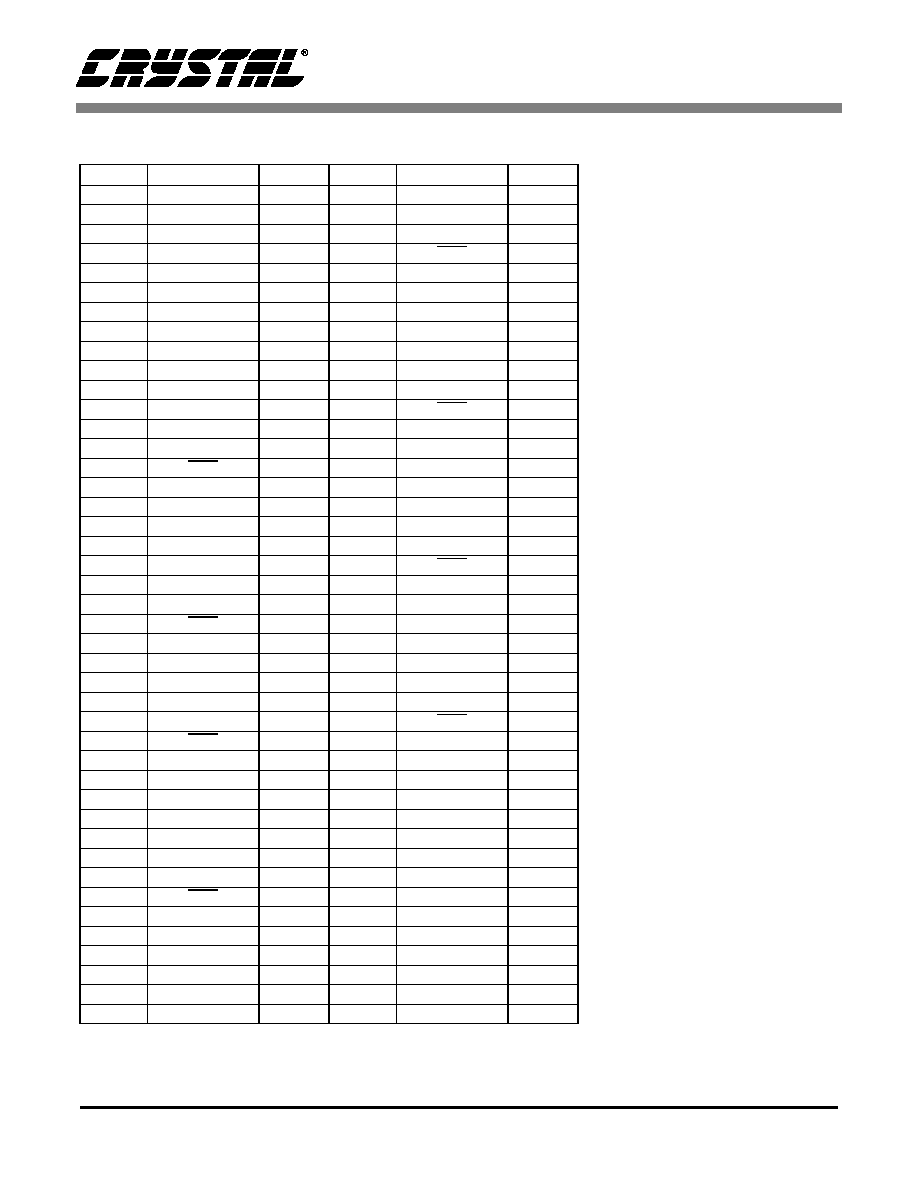
2.6 JTAG Support
The CS61881 supports the IEEE Boundary Scan
Specification as described in the IEEE 1149.1 stan-
dards. A Test Access Port (TAP) is provided that
consists of the TAP controller, the boundary scan
register (BSR), and the 5 standard pins (TRSTB,
TCK, TMS, TDI, and TDO). A block diagram of
the test access port is shown in Figure 5. The test
clock input (TCK) is used to sample input data on
TDI, and shift output data through TDO. The TMS
input is used to step the TAP controller through its
various states.
The Test Access Port consists of the Tap Control-
ler, Instruction Register, by-pass register, device
ID register, and boundary scan register. The TMS
input is used to manipulate the TAP controller to
allow loading of the instruction and data registers.
The instruction register is used to select test execu-
tion or register access. The by-pass register pro-
vides a direct connection between the TDI input
and the TDO output. The device identification reg-
ister contains an n-bit device identifier.
The Boundary Scan Register is used to support test-
ing of IC inter-connectivity. Using the Boundary
Scan Register, the digital input pins can be sampled
and shifted out on TDO. In addition, this register
can also be used to drive digital output pins to a
user defined state.
2.6.1 TAP Controller
The TAP Controller is a 16 state synchronous state
machine clocked by the rising edge of TCK. The
TMS input governs state transitions as shown in
Figure 6. The value shown next to each state tran-
sition in the diagram is the value that must be on
TMS when it is sampled by the rising edge of TCK.
CS61881
DS451PP3
11
MUX
TDI
TCK
TDO
JTAG Block
Boundary Scan Data Register
Digital output pins
Digital input pins
parallel latched
output
TAP
Controller
Instruction (shift) Register
Bypass Data Register
Device ID Data Register
parallel latched
output
TMS
TRSTB
Figure 5. Test Access Port Architecture
Test-Logic-Reset
Run-Test/Idle
Select-DR-Scan
Capture-DR
Shift-DR
Exit1-DR
Pause-DR
Exit2-DR
Update-DR
Select-IR-Scan
Capture-IR
Shift-IR
Exit1-IR
Pause-IR
Exit2-IR
Update-IR
1
0
0
1
1
0
1
0
1
1
0
1
0
0
1
0
1
0
0
1
1
0
1
1
0
1
0
0
1
0
1
0
Figure 6. TAP Controller State Diagram

CS61881
12
DS451PP3
2.6.2 Test-Logic-Reset
The test-logic-reset state is used to disable the test
logic when the part is in normal mode of operation.
This state is entered by asynchronously asserting
TRSTB or forcing TMS High for 5 TCK periods.
2.6.3 Run-Test-Idle
The run-test-idle state is used to run tests.
2.6.4 Select-DR-Scan
This is a temporary controller state.
2.6.5 Capture-DR
In this state, the Boundary Scan Register captures
input pin data if the current instruction is EXTEST
or SAMPLE/PRELOAD.
2.6.6 Shift-DR
In this controller state, the active test data register
connected between TDI and TDO, as determined
by the current instruction, shifts data out on TDO
on each rising edge of TCK.
2.6.7 Exit1-DR
This is a temporary state. The test data register se-
lected by the current instruction retains its previous
value.
2.6.8 Pause-DR
The pause state allows the test controller to tempo-
rarily halt the shifting of data through the current
test data register.
2.6.9 Exit2-DR
This is a temporary state. The test data register se-
lected by the current instruction retains its previous
value.
2.6.10 Update-DR
The Boundary Scan Register is provided with a
latched parallel output to prevent changes while
data is shifted in response to the EXTEST and
SAMPLE/PRELOAD instructions. When the TAP
controller is in this state and the Boundary Scan
Register is selected, data is latched into the parallel
output of this register from the shift-register path
on the falling edge of TCK. The data held at the
latched parallel output changes only in this state.
2.6.11 Select-IR-Scan
This is a temporary controller state. The test data
register selected by the current instruction retains
its previous state.
2.6.12 Capture-IR
In this controller state, the instruction register is
loaded with a fixed value of "01" on the rising edge
of J-TCK. This supports fault-isolation of the
board-level serial test data path.
2.6.13 Shift-IR
In this state, the shift register contained in the in-
struction register is connected between TDI and
TDO and shifts data one stage towards its serial
output on each rising edge of TCK.
2.6.14 Exit1-IR
This is a temporary state. The test data register se-
lected by the current instruction retains its previous
value.
2.6.15 Pause-IR
The pause state allows the test controller to tempo-
rarily halt the shifting of data through the instruc-
tion register.
2.6.16 Exit2-IR
This is a temporary state. The test data register se-
lected by the current instruction retains its previous
value.
2.6.17 Update-IR
The instruction shifted into the instruction register
is latched into the parallel output from the shift-reg-
ister path on the falling edge of J-TCK. When the
new instruction has been latched, it becomes the

CS61881
DS451PP3
13
current instruction. The test data registers selected
by the current instruction retain their previous val-
ue.
2.7 JTAG Instruction Register (IR)
The 2-bit instruction register selects the test to be
performed and/or the data register to be accessed.
The valid instructions are shifted in LSB first and
are listed in Table 1.
2.7.1 EXTEST
The EXTEST instruction allows testing of off-chip
circuitry and board-level interconnect. EXTEST
connects the BSR to the TDI and TDO pins.
CS61881 inputs can be sampled by loading the
BSR with the Capture DR state. The sample values
can then be viewed by shifting the BSR register us-
ing the Shift-DR state. The device output pins can
be set by shifting a pattern into the boundary scan
register and then using the Update-DR state.
2.7.2 SAMPLE/PRELOAD
The SAMPLE/PRELOAD instruction samples all
device inputs and outputs. This instruction places
the BSR between the TDI and TDO pins. The BSR
is loaded with samples of the I/O pins by the Cap-
ture-DR state.
2.7.3 IDCODE
The IDCODE instruction connects the device iden-
tification register to the TDO pin. The device iden-
tification code can then be shifted out TDO using
the Shift-DR state
2.7.4 BYPASS
The BYPASS instruction connects a one TCK de-
lay register between TDI and TDO. The instruction
is used to bypass the device.
2.8 Boundary Scan Register (BSR)
The BSR is a shift register that provides access to
the digital I/O pins. The BSR is used to read and
write the device pins to verify interchip connectiv-
ity. Each pin has a corresponding scan cell in the
register. The pin to scan cell mapping is given in
the BSR description shown in Table 2.
Notes: 1)
Data is shifted LSB first into the BSR
register.
2) HIZ controls the RPOSx, RNEGx, and
RCLKx pins. When HIZ is High, the outputs
are enabled; when HIZ is Low, the outputs
are tri-stated.
IR CODE
INSTRUCTION
000
EXTEST
100
SAMPLE/PRELOAD
110
IDCODE
111
BYPASS
Table 1. JTAG Instructions
CS61881
14
DS451PP3
BSR Bit
Pin Name
Cell Type
BSR Bit
Pin Name
Cell Type
0
LOOP0
I
43
RCLK5
O
1
LOOP1
I
44
RPOS5
O
2
LOOP2
I
45
RNEG5
O
3
LOOP3
I
46
HIZ5
note 1
4
LOOP4
I
47
ALOS5
O
5
LOOP5
I
48
TCLK4
I
6
LOOP6
I
49
TPOS4
I
7
LOOP7
I
50
TNEG4
I
8
TCLK1
I
51
RCLK4
O
9
TPOS1
I
52
RPOS4
O
10
TNEG1
I
53
RNEG4
O
11
RCLK1
O
54
HIZ4
note 1
12
RPOS1
O
55
ALOS4
O
13
RNEG1
O
56
TXOE
I
14
HIZ1
note 1
57
RPS
I
15
ALOS1
O
58
ALOS7
O
16
TCLK0
I
59
RNEG7
O
17
TPOS0
I
60
RPOS7
O
18
TNEG0
I
61
RCLK7
O
19
RCLK0
O
62
HIZ7
note 1
20
RPOS0
O
63
TNEG7
I
21
RNEG0
O
64
TPOS7
I
22
HIZ0
note 1
65
TCLK7
I
23
ALOS0
O
66
ALOS6
O
24
ALOS3
O
67
RNEG6
O
25
RNEG3
O
68
RPOS6
O
26
RPOS3
O
69
RCLK6
O
27
RCLK3
O
70
HIZ6
note 1
28
HIZ3
note 1
71
TNEG6
I
29
TNEG3
I
72
TPOS6
I
30
TPOS3
I
73
TCLK6
I
31
TCLK3
I
74
CBLSEL
I
32
ALOS2
O
33
RNEG2
O
34
RPOS2
O
35
RCLK2
O
36
HIZ2
note 1
37
TNEG2
I
38
TPOS2
I
39
TCLK2
I
40
TCLK5
I
41
TPOS5
I
42
TNEG5
I
Table 2. Boundary Scan Register

CS61881
DS451PP3
15
3. PIN DESCRIPTION
3.1 Pinout - 144-Pin LQFP
14
4
14
3
14
2
14
0
13
9
13
8
13
7
13
6
13
5
14
1
13
4
13
3
13
2
13
1
13
0
12
9
12
8
12
7
12
6
12
5
12
4
12
3
12
2
12
1
12
0
CS61881
144-Pin
LQFP
37
38
39
41
42
43
44
45
46
40
47
48
49
50
51
52
53
54
55
56
57
58
59
60
61
62
63
64
65
66
67
68
69
70
71
72
108
107
106
104
103
102
101
100
99
105
98
97
96
95
94
93
92
91
90
89
88
87
86
85
84
83
82
81
80
79
78
77
76
75
74
73
11
9
11
8
11
7
11
6
11
5
11
4
11
3
11
2
11
1
11
0
10
9
1
2
3
5
6
7
8
9
10
4
11
12
13
14
15
16
17
18
19
20
21
22
23
24
25
26
27
28
29
30
31
32
33
34
35
36
TN
E
G
7
RCL
K7
RPO
S
7
RNEG
7
AL
O
S
7
RT
I
P
7
RRI
NG
7
T
V
CC7
TTI
P
7
TR
I
N
G7
T
G
ND7
RRI
NG
6
RT
I
P
6
T
G
ND6
TR
I
N
G6
TTI
P
6
T
V
CC6
RT
I
P
5
RRI
NG
5
T
V
CC5
TTI
P
5
TR
I
N
G5
T
G
ND5
RRI
NG
4
RT
I
P
4
T
G
ND4
TR
I
N
G4
TTI
P
4
T
V
CC4
RPS
TX
OE
AL
O
S
4
RNEG
4
RPO
S
4
RCL
K4
TN
E
G
4
TPOS7
TCLK7
ALOS6
RNEG6
RPOS6
RCLK6
TNEG6
TPOS6
TCLK6
RPD#
GND
GND
GND
GND
GND
GND
VCCIO
GNDIO
RVCC0
RGND0
LOOP0
LOOP1
LOOP2
LOOP3
LOOP4
LOOP5
LOOP6
LOOP7
TCLK1
TPOS1
TNEG1
RCLK1
RPOS1
RNEG1
ALOS1
TCLK0
TPOS4
TCLK4
ALOS5
RNEG5
RPOS5
RCLK5
TNEG5
TPOS5
TCLK5
TDI
TDO
TCK
TMS
TRST
REF
CBLSEL
VCCIO
GNDIO
RVCC1
RGND1
GND
GND
GND
GND
GND
NC
NC
TCLK2
TPOS2
TNEG2
RCLK2
RPOS2
RNEG2
ALOS2
TCLK3
TPOS3
TP
OS
0
TN
E
G
0
RCL
K0
RPO
S
0
RNEG
0
AL
O
S
0
GN
D
T
V
CC0
TTI
P
0
TR
I
N
G0
T
G
ND0
RT
I
P
0
RRI
NG
0
T
G
ND1
TR
I
N
G1
TTI
P
1
T
V
CC1
RRI
NG
1
RT
I
P
1
T
V
CC2
TTI
P
2
TR
I
N
G2
T
G
ND2
RT
I
P
2
RRI
NG
2
T
G
ND3
TR
I
N
G3
TTI
P
3
T
V
CC3
RRI
NG
3
RT
I
P
3
AL
O
S
3
RNEG
3
RPO
S
3
RCL
K3
TN
E
G
3
(Top View)
Figure 7. 144-Pin LQFP Pin Description Drawing
CS61881
16
DS451PP3
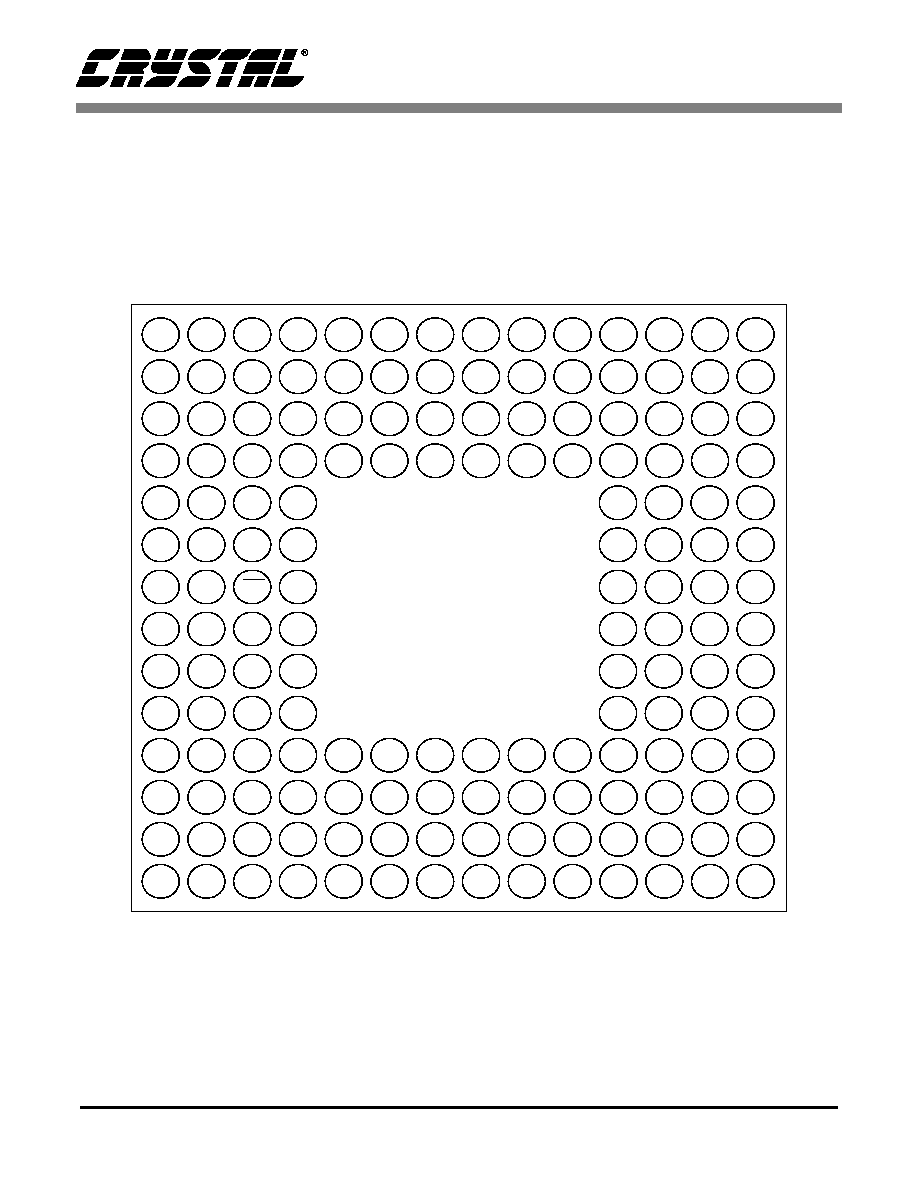
3.2 Pinout - 160-Pin FBGA
1
2
3
4
5
6
7
8
9
10
11
12
13
14
TXOE
TCK
VCCIO
RVCC
1
GND
NC
TCLK
5
RCLK
4
TCLK
4
RCLK
5
TCLK
2
RCLK
3
TCLK
3
RCLK
2
RPOS
TDO
CBLSEL
REF
GND
NC
TPOS
5
RPOS
4
TPOS
4
RPOS
5
TPOS
2
RPOS
3
TPOS
3
RPOS
2
ALOS
5
TDI
TRST
GND
GND
ALOS
2
TNEG
5
RNEG
4
TNEG
4
RNEG
5
TNEG
2
RNEG
3
TNEG
3
RNEG
2
ALOS
4
TMS
GNDIO
RGND
1
GND
ALOS
3
TVCC
5
TVCC
4
TVCC
4
TVCC
5
TVCC
2
TVCC
3
TVCC
3
TVCC
2
TTIP
5
TRING
4
TTIP
4
TRING
5
TTIP
2
TRING
3
TTIP
3
TRING
2
TGND
5
TGND
4
TGND
4
TGND
5
TGND
2
TGND
3
TGND
3
TGND
2
RRING
5
RTIP
4
RRING
4
RTIP
5
RRING
2
RTIP
3
RRING
3
RTIP
2
RRING
6
RTIP
7
RRING
7
RTIP
6
RRING
1
RTIP
0
RRING
0
RTIP
1
TGND
6
TGND
7
TGND
7
TGND
6
TGND
1
TGND
0
TGND
0
TGND
1
TTIP
6
TRING
7
TTIP
7
TRING
6
TTIP
1
TRING
0
TTIP
0
TRING
1
TVCC
6
TVCC
7
TVCC
7
TVCC
6
TVCC
1
TVCC
0
TVCC
0
TVCC
1
ALOS
7
GND
GNDIO
LOOP
3
ALOS
0
RGND
0
TNEG
6
RNEG
7
TNEG
7
RNEG
6
TNEG
1
RNEG
0
TNEG
0
RNEG
1
ALOS
6
GND
GND
LOOP
4
ALOS
1
LOOP
1
TPOS
6
RPOS
7
TPOS
7
RPOS
6
TPOS
1
RPOS
0
TPOS
0
RPOS
1
GND
GND
LOOP
0
LOOP
5
GND
LOOP
2
TCLK
6
RCLK
7
TCLK
7
RCLK
6
TCLK
1
RCLK
0
TCLK
0
RCLK
1
RPD#
GND
VCCIO
LOOP
6
LOOP
7
RVCC
0
1
2
3
4
5
6
7
8
9
10
11
12
13
14
A
B
C
D
E
F
G
H
J
K
L
M
N
P
A
B
C
D
E
F
G
H
J
K
L
M
N
P
CS61881
160 FBGA
(Bottom View)
Figure 8. 160-Pin FBGA Pin Description Drawing

CS61881
DS451PP3
17
3.3 Pin Descriptions
Power Supplies
VCCIO - Power Supply, Digital Interface, LQFP Pins 17 & 92, BGA Pins G1 & G14.
Power supply for digital interface pins; typically +3.3 Volts.
GNDIO - Ground, Digital Interface, LQFP Pins 18 & 91. BGA Pins G4 & G11.
Power supply ground for the digital interface; typically 0 Volts.
RVCC0, RVCC1 - Power Supply, Core Circuitry, LQFP Pins 19 & 90. BGA Pins H1 & H14.
Power supply for all subcircuits except the transmit driver; typically +3.3 Volts
RGND0, RGND1 - Ground, Core Circuitry, LQFP Pins 20 & 89, BGA Pins H4 & H11.
Ground for subcircuits except the transmit driver; typically 0.0 Volts
TVCC0 - Power Supply, Transmit Driver 0, LQFP Pin 44, BGA Pins N4, P4.
Power supply for transmit driver 0; typically +3.3 Volts.
TGND0 - Ground, Transmit Driver 0, LQFP Pin 47, BGA Pins N6, P6.
Power supply ground for transmit driver 0; typically 0 Volts.
TVCC1 - Power Supply, Transmit Driver 1, LQFP Pin 53, BGA Pins L4, M4.
TGND1 - Ground, Transmit Driver 1, LQFP Pin 50, BGA Pins L6, M6.
TVCC2 - Power Supply, Transmit Driver 2, LQFP Pin 56, BGA Pins L11, M11.
TGND2 - Ground, Transmit Driver 2, LQFP Pin 59, BGA Pins L9, M9.
TVCC3 - Power Supply, Transmit Driver 3, LQFP Pin 65, BGA Pins N11, P11.
TGND3 - Ground, Transmit Driver 3, LQFP Pin 62, BGA Pins N9, P9.
TVCC4 - Power Supply, Transmit Driver 4, LQFP Pin 116, BGA Pins A11, B11.
TGND4 - Ground, Transmit Driver 4, LQFP Pin 119, BGA Pins A9, B9.
TVCC5 - Power Supply, Transmit Driver 5, LQFP Pin 125, BGA Pins C11, D11.
TGND5 - Ground, Transmit Driver 5, LQFP Pin 122, BGA Pins C9, D9.
TVCC6 - Power Supply, Transmit Driver 6, LQFP Pin 128, BGA Pins C4, D4.
TGND6 - Ground, Transmit Driver 6, LQFP Pin 131, BGA Pins C6, D6.
TVCC7 - Power Supply, Transmit Driver 7, LQFP Pin 137, BGA Pins A4, B4.
TGND7 - Ground, Transmit Driver 7, LQFP Pin 134, BGA Pins A6, B6.
GND - Ground, LQFP Pins 11-16, 43, 84-88, BGA Pins E2, F1-F4, G3, K2, J11-14, H12.
Connect these pins to ground to insure proper operation.

CS61881
18
DS451PP3
Control
RPD - Receiver Power Down, LQFP Pin 10, BGA Pin E1
When RPD is Low, the complete receive path for all ports is powered down the output pins
RPOS, RNEG and RCLK are switched to the high impedance state.
TXOE - Transmitter Output Enable, LQFP Pin 114, BGA Pin E14
When TXOE is asserted Low, all of the TX drivers are forced to a high impedance state in
1
µ
S (max). All other internal circuitry remains active.
RPS - Receiver Polarity Select, LQFP Pin 115, BGA Pin E13
This pin is used to set the polarity of RPOS/RNEG. When RPS is High, RPOS/RNEG has an
active high output polarity. When RPS is low, RPOS/RNEG have an active Low polarity.
LOOP0 - Loopback Mode Select Port #0, LQFP Pin 21, BGA Pin G2
This pin selects the loopback mode for LIU transceiver 0. The mode is selected as follows:
No Loopback - LOOP0 is left open (unconnected)
Local Loopback - LOOP0 is tied High. In this mode, data transmitted on TTIP0 and TRING0
is looped back into port 0's receiver and output on RPOS0 and RNEG0. Data present on RTIP0
and RRING0 is ignored.
Remote Loopback - LOOP0 is tied Low. In this mode, data received on RTIP0 and RRING0 is
looped back for retransmission on TTIP0 and TRING0. Data on TPOS0 and TNEG0 is
ignored.
LOOP1 - Loopback Mode Select Port #1, LQFP Pin 22, BGA Pin H3
LOOP2 - Loopback Mode Select Port #2, LQFP Pin 23, BGA Pin H2
LOOP3 - Loopback Mode Select Port #3, LQFP Pin 24, BGA Pin J4
LOOP4 - Loopback Mode Select Port #4, LQFP Pin 25, BGA Pin J3
LOOP5 - Loopback Mode Select Port #5, LQFP Pin 26, BGA Pin J2
LOOP6 - Loopback Mode Select Port #6, LQFP Pin 27, BGA Pin J1
LOOP7 - Loopback Mode Select Port #7, LQFP Pin 28, BGA Pin K1

CS61881
DS451PP3
19
CBLSEL - Cable Impedance Select, LQFP Pin 93, BGA Pin G13
This pin is used to select the impedance matching network used by all eight transceivers. The
transmitters always make use of an internal cable matching network to eliminate external line
matching component. The receiver can be operated with either internal or external line
matching. The CBLSEL input sets the desired cable matching for the transmitter and configures
the receiver for either internal or external impedance matching. The Application section
provides sample schematics for both internal and external RX matching.
Status
ALOS0 - Analog Loss Of Signal Output Port #0, LQFP Pin 42, BGA Pin K4
ALOS0 is asserted "high" to indicate analog loss of signal (LOS) compliant to ITU-T G.775.
ALOS1 - Analog Loss Of Signal Port #1, LQFP Pin 35, BGA Pin K3
ALOS2 - Analog Loss Of Signal Port #2, LQFP Pin 75, BGA Pin K12
ALOS3 - Analog Loss Of Signal Port #3, LQFP Pin 68, BGA Pin K11
ALOS4 - Analog Loss Of Signal Port #4, LQFP Pin 113, BGA Pin E11
ALOS5 - Analog Loss Of Signal Port #5, LQFP Pin 106, BGA Pin E12
ALOS6 - Analog Loss Of Signal Port #6, LQFP Pin 3, BGA Pin E3
ALOS7 - Analog Loss Of Signal Port #7, LQFP Pin 140, BGA Pin E4
RX/TX Data I/O
TCLK0 - Transmit Clock Input, LQFP Pin 36, BGA Pin N1.
If a 2.048MHz transmit clock is input on this pin, the TPOS and TNEG inputs function as NRZ
inputs. In this mode, the falling edge of TCLK samples NRZ encoded data on TPOS and
TNEG.
If TCLK0 is held High, the TPOS and TNEG inputs function as RZ inputs. In this mode, the
transmit pulse width is set by the duty cycle of the signal input on TPOS and TNEG. To enter
this mode, TCLK must be held high for at least 12
µ
S.
If TCLK0 is held low for at least 12
µ
S, the output drivers enter a low-power, high impedance
state.
CBLSEL
Cable
TX Match
RX Matching Mode
No Connect
120
120
Supports both Internal and External 120
Matching
HIGH
75
75
Internal 75
Matching
LOW
75
75
External 75
Matching

CS61881
20
DS451PP3
TPOS0 - Transmit Positive Pulse Input, LQFP Pin 37, BGA Pin N2.
TNEG0 - Transmit Negative Pulse Input, LQFP Pin 38, BGA Pin N3.
When TCLK0 is active (NRZ input mode), data on TPOS0 and TNEG0 is sampled on the
falling edge of TCLK0 and transmitted onto the line at TTIP0 and TRING0 respectively. An
input on TPOS0 results in transmission of a positive pulse; an input on TNEG0 results in
transmission of a negative pulse.
When TCLK0 is held high (RZ input mode), the pulse widths of TPOS0 and TNEG0
determine the pulse widths output on TTIP0 and TRING0. If TPOS0 and TRING0 are high at
the same time, TTIP0 and TRING0 will both be 0.
RCLK0 - Receive Clock Output, LQFP Pin 39, BGA Pin P1.
This output is the XOR of RPOS and RNEG. It can be used for external clock recovery
circuits. This output is in a high-impedance state when RPD is Low.
RPOS0 - Receive Positive Pulse Output, LQFP Pin 40, BGA Pin P2.
RNEG0 - Receive Negative Pulse Output, LQFP Pin 41, BGA Pin P3.
These pins output the RZ data recovered by the receive slicers. A positive pulse on RTIP with
respect to RRING generates a logic 1 on RPOS; a positive pulse on RRING with respect to
RTIP generates a logic 1 on RNEG. The polarity of the output on RPOS/RNEG is selectable
with the RPS pin. Note: RPOS and RNEG will be active when the transceiver is in LOS.
RPOS/RNEG will be in a high impedance state if the RPD pin is Low.
TCLK1 - Transmit Clock Input Port 1, LQFP Pin 29, BGA Pin L1.
TPOS1 - Transmit Positive Pulse Input, LQFP Pin 30, BGA Pin L2.
TNEG1 - Transmit Negative Pulse Input, LQFP Pin 31, BGA Pin L3.
RCLK1 - Receive Clock Output, LQFP Pin 32, BGA Pin M1.
RPOS1 - Receive Positive Pulse Output, LQFP Pin 33, BGA Pin M2.
RNEG1 - Receive Negative Pulse Output, LQFP Pin 34, BGA Pin M3.
TCLK2 - Transmit Clock Input Port 2, LQFP Pin 81, BGA Pin L14.
TPOS2 - Transmit Positive Pulse Input, LQFP Pin 80, BGA Pin L13.
TNEG2 - Transmit Negative Pulse Input, LQFP Pin 79, BGA Pin L12.
RCLK2 - Receive Clock Output, LQFP Pin 78, BGA Pin M14.
RPOS2 - Receive Positive Pulse Output, LQFP Pin 77, BGA Pin M13.
RNEG2 - Receive Negative Pulse Output, LQFP Pin 76, BGA Pin M12.
TCLK3 - Transmit Clock Input Port 3, LQFP Pin 74, BGA Pin N14.
TPOS3 - Transmit Positive Pulse Input, LQFP Pin 73, BGA Pin N13.
TNEG3 - Transmit Negative Pulse Input, LQFP Pin 72, BGA Pin L2.
RCLK3 - Receive Clock Output, LQFP Pin 71, BGA Pin P14.
RPOS3 - Receive Positive Pulse Output, LQFP Pin 70, BGA Pin P13.
RNEG3 - Receive Negative Pulse Output, LQFP Pin 69, BGA Pin P12.

CS61881
DS451PP3
21
TCLK4 - Transmit Clock Input Port 4, LQFP Pin 107, BGA Pin B14.
TPOS4 - Transmit Positive Pulse Input, LQFP Pin 108, BGA Pin B13.
TNEG4 - Transmit Negative Pulse Input, LQFP Pin 109, BGA Pin B12.
RCLK4 - Receive Clock Output, LQFP Pin 110, BGA Pin A14.
RPOS4 - Receive Positive Pulse Output, LQFP Pin 111, BGA Pin A13.
RNEG4 - Receive Negative Pulse Output, LQFP Pin 112, BGA Pin A12.
TCLK5 - Transmit Clock Input Port 5, LQFP Pin 100, BGA Pin D14
TPOS5 - Transmit Positive Pulse Input, LQFP Pin 101, BGA Pin D13.
TNEG5 - Transmit Negative Pulse Input, LQFP Pin 102, BGA Pin D12.
RCLK5 - Receive Clock Output, LQFP Pin 103, BGA Pin C14.
RPOS5 - Receive Positive Pulse Output, LQFP Pin 104, BGA Pin C13.
RNEG5 - Receive Negative Pulse Output, LQFP Pin 105, BGA Pin C12.
TCLK6 - Transmit Clock Input Port 6, LQFP Pin 9, BGA Pin D1.
TPOS6 - Transmit Positive Pulse Input, LQFP Pin 8, BGA Pin D2.
TNEG6 - Transmit Negative Pulse Input, LQFP Pin 7, BGA Pin D3.
RCLK6 - Receive Clock Output, LQFP Pin 6, BGA Pin C1.
RPOS6 - Receive Positive Pulse Output, LQFP Pin 5, BGA Pin C2.
RNEG6 - Receive Negative Pulse Output, LQFP Pin 4, BGA Pin C3.
TCLK7 - Transmit Clock Input Port 7, LQFP Pin 2, BGA Pin B1.
TPOS7 - Transmit Positive Pulse Input, LQFP Pin 1, BGA Pin B2.
TNEG7 - Transmit Negative Pulse Input, LQFP Pin 144, BGA Pin B3.
RCLK7 - Receive Clock Output, LQFP Pin 143, BGA Pin A1.
RPOS7 - Receive Positive Pulse Output, LQFP Pin 142, BGA Pin A2.
RNEG7 - Receive Negative Pulse Output, LQFP Pin 141, BGA Pin A3.
TTIP0 - Transmit Tip Output, LQFP Pin 45, BGA Pin N5.
TRING0 - Transmit Ring Output, LQFP Pin 46, BGA Pin P5.
These pins are the output of the differential transmit driver. The driver matches impedances for
75
unbalanced and 120
balanced lines requiring only a 1:1.15 transformer. The CBLSEL
pin is used to select the appropriate impedance for line matching.
Note: TTIP and TRING are forced to a high impedance state when the TCLK pin is Low for
over 12
µ
S.
RTIP0 - Receive Tip Input, LQFP Pin 48, BGA Pin P7.
RRING0 - Receive Ring Input, LQFP Pin 49, BGA Pin N7.
The pins are the differential line inputs to the receiver. The receiver internally matches
impedances for 75
unbalanced and 120
balanced lines requiring only a 1:2 transformer,
two external 15
resistors, and one capacitor. The CBLSEL pin is used to select the
appropriate impedance for line matching.
Data recovered from the signal input on these pins is output via RPOS, RNEG, and RCLK.

CS61881
22
DS451PP3
TTIP1 - Transmit Tip Output, LQFP Pin 52, BGA Pin L5.
TRING1 - Transmit Ring Output, LQFP Pin 51, BGA Pin M5.
RTIP1 - Receive Tip Output, LQFP Pin 55, BGA Pin M7.
RRING1 - Receive Ring Output, LQFP Pin 54, BGA Pin L7.
TTIP2 - Transmit Tip Output, LQFP Pin 57, BGA Pin L10.
TRING2 - Transmit Ring Output, LQFP Pin 58, BGA Pin M10.
RTIP2 - Receive Tip Output, LQFP Pin 60, BGA Pin M8.
RRING2 - Receive Ring Output, LQFP Pin 61, BGA Pin L8.
TTIP3 - Transmit Tip Output, LQFP Pin 64, BGA Pin N10.
TRING3 - Transmit Ring Output, LQFP Pin 63, BGA Pin P10.
RTIP3 - Receive Tip Output, LQFP Pin 67, BGA Pin P8.
RRING3 - Receive Ring Output, LQFP Pin 66, BGA Pin N8.
TTIP4 - Transmit Tip Output, LQFP Pin 117, BGA Pin B10.
TRING4 - Transmit Ring Output, LQFP Pin 118, BGA Pin A10.
RTIP4 - Receive Tip Output, LQFP Pin 120, BGA Pin A8.
RRING4 - Receive Ring Output, LQFP Pin 121, BGA Pin B8.
TTIP5 - Transmit Tip Output, LQFP Pin 124, BGA Pin D10.
TRING5 - Transmit Ring Output, LQFP Pin 123, BGA Pin C10.
RTIP5 - Receive Tip Output, LQFP Pin 127, BGA Pin C8.
RRING5 - Receive Ring Output, LQFP Pin 126, BGA Pin D8.
TTIP6 - Transmit Tip Output, LQFP Pin 129, BGA Pin D5.
TRING6 - Transmit Ring Output, LQFP Pin 130, BGA Pin C5.
RTIP6 - Receive Tip Output, LQFP Pin 132, BGA Pin C7.
RRING6 - Receive Ring Output, LQFP Pin 133, BGA Pin D7.
TTIP7 - Transmit Tip Output, LQFP Pin 136, BGA Pin B5.
TRING7 - Transmit Ring Output, LQFP Pin 135, BGA Pin A5.
RTIP7 - Receive Tip Output, LQFP Pin 139, BGA Pin A7.
RRING7 - Receive Ring Output, LQFP Pin 138, BGA Pin B7.
JTAG Test Interface
TRST - JTAG Reset, LQFP Pin 95, BGA Pin G12.
This active low input resets the JTAG controller. This input is pulled up internally and may be
left as a NC.
TMS - JTAG Test Mode Select Input, LQFP Pin 96, BGA Pin F11.
This input enables the JTAG serial port when active high. This input is sampled on the rising
edge of JTCK. This input is pulled up internally and may be left as a NC.

CS61881
DS451PP3
23
TCK - JTAG Test Clock, LQFP Pin 97, BGA Pin F14.
Data on TDI is valid on the rising edge of TCK. Data on TDO is valid on the falling edge of
TCK. When TCK is stopped high or low, the contents of all JTAG registers remain unchanged.
Tie low when not used.
TDO- JTAG Test Data Output, LQFP Pin 98, BGA Pin F13.
TAG test data is shifted out of the device on this pin. Data is output on the falling edge of
TCK. Leave as NC when not used.
TDI- JTAG Test Data Input, LQFP Pin 99, BGA Pin F12.
JTAG test data is shifted into the device using this pin. The pin is sampled on the rising edge
of TCK. TDI is pulled up internally and may be left as a NC when not used.
Miscellaneous
REF - Reference Output, LQFP Pin 94, BGA Pin H13.
This pin must be tied to ground through 13.3 k
1% resistor.
No Connects
NC - No Connects, LQFP Pin 82-83, BGA Pin K13-K14.
CS61881
24
DS451PP3
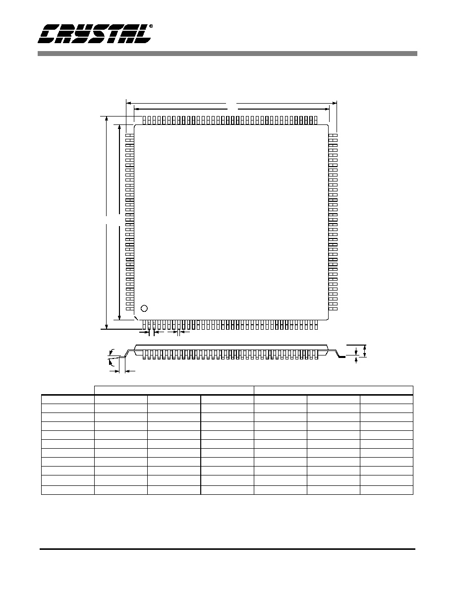
4. PACKAGE DIMENSIONS
INCHES
MILLIMETERS
DIM
MIN
NOM
MAX
MIN
NOM
MAX
A
---
0.55
0.063
---
1.40
1.60
A1
0.002
0.004
0.006
0.05
0.10
0.15
B
0.007
0.008
0.011
0.17
0.20
0.27
D
0.854
0.866 BSC
0.878
21.70
22.0 BSC
22.30
D1
0.783
0.787 BSC
0.791
19.90
20.0 BSC
20.10
E
0.854
0.866 BSC
0.878
21.70
22.0 BSC
22.30
E1
0.783
0.787 BSC
0.791
19.90
20.0 BSC
20.10
e*
0.016
0.020
0.024
0.40
0.50 BSC
0.60
0.000∞
4∞
7.000∞
0.00∞
4∞
7.00∞
L
0.018
0.024
0.030
0.45
0.60
0.75
* Nominal pin pitch is 0.50 mm
Controlling dimension is mm.
JEDEC Designation: MS022
144L LQFP PACKAGE DRAWING
E1
E
D1
D
1
e
L
B
A1
A

CS61881
DS451PP3
25
Notes: 14. All dimensions and tolerance conform to ASME Y 14.5 M - 1994.
Dimension is measured at the maximum solder ball diameter, parallel to primary datum
.
Primary datum
and seating plane are defined by the spherical crowns of the solder balls.
4. Maximum mold to substrate offset shall be 0.127.
5. The surface finish of the package shall be EDM charmille #18 - #21.
6. Unless otherwise specified tolerance: Decimal ±0.05; Angular ±2
JEDEC #: MO-158
TOP VIEW
BOTTOM VIEW
A
B
C
D
E
F
G
H
I
J
K
L
M
Pin #A1 Corner
14 13 12 11 10
9
8
7
6
5
4
3
21
4.72 ± 0.10
1.00 REF
4.72 ±0.10
1.00 REF
15.00/M+3A1BE0.20
13.00 ± 0.20
13.00 ± 0.20
Pin #A1 Identifier (shiny)
1.00x0.15 Depth
8xR0.5
3x
1.00
4x1.20x45
0.20 (4x)
A
13.00
1.00
0.50 ± 0.10
1.00
13.00
2
0.30 C A B
0.10 C
M
SIDE VIEW
1.61 ± 0.19
0.40 ± 0.10
0.85
0.36 ± 0.04
0.1
5
C
C
Seating Plane
3
B
15.00/M+3A1BE0.20
A
A
3.0∞
160-BALL FBGA (2 LAYER) PACKAGE DRAWING
C
C
2
3

CS61881
26
DS451PP3
5. APPLICATIONS
+
RGND
+3.3V
RV+
T1 1:2
REF
CS61881
One
Channel
TRANSMIT
LINE
T2 1:1.15
R1
R2
13.3k
GND
CBLSEL
TV+
VCCIO
+3.3V
+
0.1
µ
F
TGND
+
GNDIO
NC
120
Cable
+3.3V
Note 1
Note 2
RECEIVE
LINE
RTIP
RRING
TRING
TTIP
0.1
µ
F
0.1
µ
F
68
µ
F
0.1
µ
F
75
Cable
Figure 9. Internal RX Impedance Matching
Notes: 1) Required Capacitor between each TVCC, RVCC, VCCIO and TGND, RGND, GNDIO respectively.
2) Common decoupling capacitor for all TVCC and TGND pins.
Component
75
Coaxial Cable
120
Coaxial Cable
R1 (
)
15
15
R2 (
)
15
15

CS61881
DS451PP3
27
+
RGND
+3.3V
RV+
T1
1:2
REF
CS61881
On
e Ch
an
nel
TRANSMIT
LINE
T2 1:1.15
GND
NC
GND
CBLSEL
TV+
VCCIO
+3.3V
+
TGND
+
GNDIO
R1
R2
1k
1k
13.3k
Note 1
Note 2
0.1
µ
F
68
µ
F
0.1
µ
F
0.1
µ
F
RECEIVE
LINE
RTIP
RRING
TRING
TTIP
120
Cable
75
Cable
0.1
µ
F
Figure 10. External RX Impedance Matching
Notes: 1) Required Capacitor between each TVCC, RVCC, VCCIO and TGND, RGND, GNDIO respectively.
2) Common decoupling capacitor for all TVCC and TGND pins.
Component
E1 75
Coaxial Cable
E1 120
Twisted Pair Cable
R1 (
)
9.31
15
R2 (
)
9.31
15