
Features
∑
Monolithic T1 Framing Device
∑
Both Framers Support SF(D4
Æ
) and
ESF Framing Formats
∑
CS62180B Supports SLC-96
Æ
and
T1DM Framing Formats
∑
CS62180B Contains Updated AIS and
Carrier Loss Detection Criteria
∑
CS62180B is Pin Compatible with
CS62180A, DS2180A, and DS2180
General Description
The CS62180A and CS62180B are monolithic CMOS
devices which encode and decode T1 framing formats.
The devices support bit-seven and B8ZS zero suppres-
sion, and bit-robbed signaling. Clear channel mode can
be selected on a per channel basis.
The serial interface has been enhanced to allow the
CS62180A and CS62180B to share a chip select sig-
nal and register address space with the CS61535A,
CS61574A, and CS61575 Line Interface Units.
Applications
∑
T1 Line Cards
∑
ISDN Primary Rate Line Cards
Ordering Information:
CS62180A-IP 40 Pin Plastic DIP
-40 to 85
∞
C
CS62180A-IL 44 Pin PLCC
-40 to 85
∞
C
CS62180B-IP 40 Pin Plastic DIP
-40 to 85
∞
C
CS62180B-IL 44 Pin PLCC
-40 to 85
∞
C
MAY'96
DS225PP1
1
Crystal Semiconductor Corporation
P.O. Box 17847, Austin, TX 78760
(512) 445-7222 FAX: (512) 445-7581
T1 Framer
CS62180A
CS62180B
Serial
Interface
Registers
Control
VDD
VSS
TEST
TSER TABCD
TSIGSEL
TMO
TCHCLK
TSIGFR
TPOS
TNEG
TMSYNC
TFSYNC
Transmit Timing
Data
Selector
F-Bit Data
Yellow Alarm
Bipolar
Coder
Transmitter
Data
DeMUX
Synchronizer
RLOS
RBV
RCL
RPOS
RNEG
RFER
RCLK
RMSYNC RFSYNC
Code Gen.
Receive Sync
Controller
CRC
Receiver
Receive
Timing
Bipolar
Decoder
SCLK
SDI
SDO
SPS
RSER
RABCD
RLINK
RLCLK
RSIGFR
RSIGSEL
RCHCLK
TCLK
TLCLK
TLINK
CS
INT
RST
3
11
10
28
27
39
37
36
34
35
38
24
7
6
4
8
12
13
40
20
33
32
1
2
5
9
14
17
18
15
16
19
26
29
22
23
30
31
25
Alarm
Detect
RYEL
21
RBL (CS2180B-IL only)
CRC
Copyright
©
Crystal Semiconductor Corporation 1996
(All Rights Reserved)

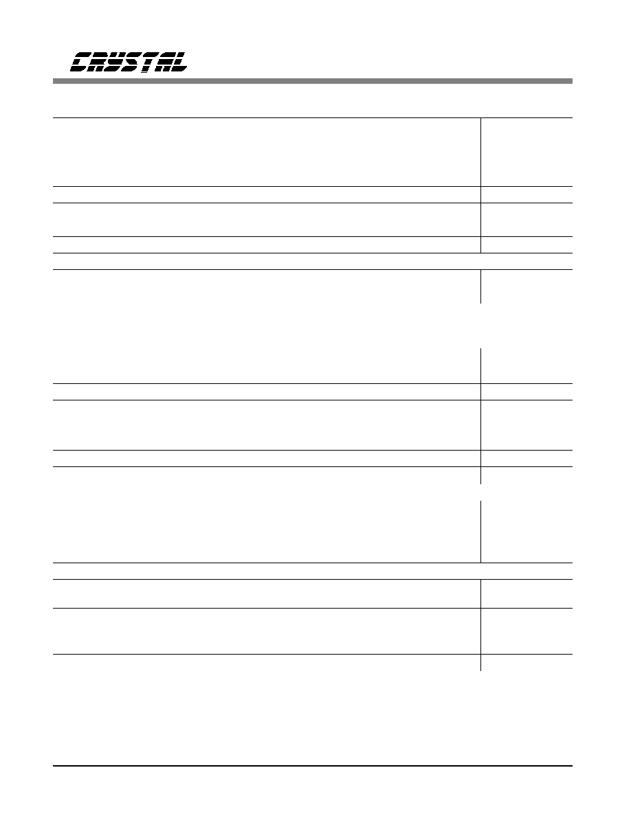
ABSOLUTE MAXIMUM RATINGS
Parameter
Symbol
Min
Typ
Max
Units
DC Supply
(Referenced to GND)
V
DD
-
-
6.0
V
Input voltage, any pin
(Referenced to GND)
V
IN
-1.0
-
+7
V
Input Current, any pin
(Note 1)
I
IN
-10
-
+10
mA
Ambient Operating Temperature
T
A
-40
-
85
∞C
Storage Temperature
T
STG
-65
-
150
∞C
Soldering Temperature for 10 s.
-
-
-
260
∞C
Notes: 1. Transient current of up to 100 mA will not cause SCR latch-up.
WARNING:
Operation at or beyond these limits may result in permanent damage to the device.
Normal operation is not guaranteed at these extremes.
RECOMMENDED OPERATING CONDITIONS
Parameter
Symbol
Min
Typ
Max
Units
DC Voltage
V
DD
4.5
5.0
5.5
V
Supply Current
(Notes 2 and 3)
I
DD
-
3
10
mA
Ambient Operating Temperature
T
A
-40
25
85
∞C
Power Consumption
(Notes 2 and 3)
P
C
-
15
85
mW
Notes: 2. TCLK = RCLK = 1.544 MHz. If RCLK is static and RST is high, I
DD
will typically be 1.0 mA.
3. Outputs open.
DIGITAL CHARACTERISTICS (T
A
= -40 to 85 ∞C; V
DD
= 5.0 V
±
10%; GND = 0 V)
Parameter
Symbol
Min
Typ
Max
Units
High-Level Input Voltage
(Note 4)
V
IH
2.0
-
V
DD
+0.3
V
Low-Level Input Voltage
H
IL
-0.3
-
+0.8
V
High-level Output Voltage
(Note 5)
V
OH
V
DD
- 1.0
-
-
V
Low-Level Output Voltage
(IOUT = 1.6 mA)
V
OL
-
-
0.4
V
Output Current @ 2.4 V
(Note 6)
I
OH
-
-
-1
mA
Output Current @ 0.4 V
(Note 7)
I
OL
+4
-
-
mA
Input Leakage Current
I
IL
-
-
1
µ
A
Output Leakage Current
(Note 8)
I
LO
-
-
1
µ
A
Input Capacitance
C
IN
-
-
5
pF
Output Capacitance
C
OUT
-
-
7
pF
Notes: 4. V
IH
(min) = 2.2 V for V
DD
= 5.25 to 5.5 V and T
A
> 70 ∞C.
5. I
OUT
= -100
µ
A. This guarantees the ability to drive one TTL load (V
OH
= 2.4 V @ I
OUT
= -40
µ
A).
6. All outputs except INT, which is open drain.
7. All outputs.
8. Applies to SDO when tristated.
CS62180A
CS62180B
2
DS225PP1

SCLK
SDO
MSB
High-Z
High-Z
CS
CDZ
t
CDV
t
CDH2
t
Serial Port Read Timing
13. Serial port write must precede a port read to provide address information.
14. SDO will go High-Z: 1) if CS returns high at anytime; 2) after outputing MSB.
SCLK
SDI
LSB
LSB
MSB
Control Byte
Data Byte
DC
t
CC
t
CH
t
CDH1
t
CD
t
CL
t
CDH1
t
CCH
t
CWH
t
CS
Serial Port Write Timing
11. For the CS62180A only, data bytes must be valid across low clock periods to prevent transients in
operating modes. t
CD
is not a requirement for the CS62180B. In the CS62180B data is latched on the
rising edge of SCLK.
12. Shaded regions indicate
don't care states.
SWITCHING CHARACTERISTICS - SERIAL PORT
(T
A
= -40 to 85
∞
C; V
DD
= 5V
±
10%; V
IH
= 2.0V; V
IL
= 0.8V; Maximum input rise & fall times of 10 ns)
Parameter
Symbol
Min
Typ
Max
Units
SDI to SCLK Setup
t
DC
50
-
-
ns
SCLK to SDI Hold
t
CDH1
50
-
-
ns
SDI to SCLK Falling Edge (Applies to CS62180A)
t
CD
50
-
-
ns
SCLK Low Time
t
CL
250
-
-
ns
SCLK High Time
t
CH
250
-
-
ns
SCLK Rise & Fall Times
(Note 9)
t
R
, t
F
-
-
500
ns
CS to SCLK Set up
t
CC
50
-
-
ns
SCLK to CS Hold
t
CCH
50
-
-
ns
CS Inactive Time
t
CWH
250
-
-
ns
SCLK to SDO Valid
(Note 9)
t
CDV
-
-
200
ns
SCLK Rising to MSB of SDO Hold
(Note 10)
t
CDH2
25
-
-
ns
CS to SDO High-Z
t
CDZ
-
-
75
ns
Notes: 9. Output load capacitance = 100 pF.
10. SDO goes High-Z after rising edge of SCLK for MSB, regardless of the state of CS.
CS62180A
CS62180B
DS225PP1
3
Notes:15. Average reframe time is the time from the rising edge of RLOS until the rising edge of RMSYNC
which updates the receiver output timing.
16. With error free data.
SWITCHING CHARACTERISTICS - TRANSMITTER
(T
A
= -40 to 85
∞
C; V
DD
= 5V
±
10%; V
IH
= 2.0V; V
IL
= 0.8V; Maximum input rise & fall times of 10 ns)
Parameter
Symbol
Min
Typ
Max
Units
TCLK Period
t
P
250
648
-
ns
TCLK Pulse Width
t
WL
, t
WH
125
324
-
ns
TCLK Rise & Fall Times
t
F
, t
R
-
20
-
ns
TSER, TABCD, TLINK Setup to TCLK Falling
t
STD
50
-
-
ns
TSER, TABCD, TLINK Hold from TCLK Falling
t
HTD
50
-
-
ns
TFSYNC, TMSYNC Setup to TCLK Rising
t
STS
-125
-
125
ns
TFSYNC, TMSYNC Pulse Width
t
TSP
100
-
-
ns
Propagation Delays
TFSYNC to TMO, TSIGSEL, TSIGFR, TLCLK
t
PTS
-
-
75
ns
TCLK Rising to TCHCLK
t
PTCH
-
-
75
ns
SWITCHING CHARACTERISTICS - RECEIVER
(T
A
= -40 to 85
∞
C; V
DD
= 5V
±
10%; V
IH
= 2.0V; V
IL
= 0.8V; Maximum input rise & fall times of 10 ns)
Parameter
Symbol
Min
Typ
Max
Units
Transition Time, All Outputs
t
TTR
-
-
20
ns
RCLK Period
t
P
250
648
-
ns
RCLK Pulse Width
t
WL
, t
WH
100
324
-
ns
RCLK Rise & Fall Times
t
F
, t
R
-
20
-
ns
RPOS, RNEG Setup to RCLK Falling
t
SRD
50
-
-
ns
RPOS, RNEG Hold to RCLK Falling
t
HRD
50
-
-
ns
Minimum RST Pulse Width on System Power Up or Restart
t
RST
1
-
-
µ
s
Propagation Delays
RCLK to RMSYNC, RFSYNC,RSIGSEL,
RSIGFR, RLCLK, RCHCLK
t
PRS
-
-
75
ns
RCLK to RSER, RABCD, RLINK
t
PRD
-
-
75
ns
RCLK to RYEL, RCL, RFER, RLOS, RBV
t
PRA
-
-
75
ns
Average Reframe Time
(Notes 15 and 16)
193S
RCR.2 = 0
RCR.2 = 1
t
RS
-
-
3.75
7.25
-
-
ms
ms
193E
RCR.2 = 0
RCR.2 = 1
t
RS
-
-
7.5
14.5
-
-
ms
ms
T1DM
t
RS
-
750
-
µ
s
SLC-96
Æ
t
RS
-
6.0
-
ms
CS62180A
CS62180B
4
DS225PP1

TCLK
TCHCLK
TMO, TLCLK,
TSIGSEL
TSIGFR
TFSYNC,
TMSYNC
TSER,
TABCE,
TLINK
TLCLK
STD
t
HTD
t
WH
t
WL
t
P
t
STS
t
PTS
t
TSP
t
PTCH
t
Transmitter Timing.
Note: TMO, TLCLK, TSIGSEL and TSIGFR are generally coincident with the
rising edge of TCLK.
10%
90%
t
R
F
t
Logic 0
Logic 1
VDD - 1.0 V
0.4 V
TTR
t
Transition Times for All Receiver Outputs.
Old Alignment
New Alignment
RLOS
RMSYNC
t
RS
Rise and Fall Times for RCLK & TCLK.
Reframe Timing.
CS62180A
CS62180B
DS225PP1
5

WH
t
WL
t
P
t
PRD
t
RCLK
RSER, RABCD
SRD
t
HRD
t
RST
t
PRA
t
RFSYNC, RMSYNC,
RSIGSEL, RSIGFR
RLCLK, RCHCLK
RPOS, RNEG
RYEL, RCL, RBV,
RFER, RLOS
RST
(RFSYNC)
PRS
t
t
P
RLINK
Receiver Timing.
CS62180A
CS62180B
6
DS225PP1

GENERAL DESCRIPTION
The CS62180A is a monolithic CMOS circuit
that encodes and decodes T1 (1.544 MHz) digi-
tal transmission formats for SF(D4
Æ
) (193S: 12
frames per superframe), and ESF (193E: 24
frames per superframe) framing formats. The
CS62180B also encodes and decodes the SLC-
96
Æ
(SLC-96
Æ
: 72 frames per superframe) and
DDS
Æ
T1DM (T1DM: 12 frames per superframe
plus unique channel number 24) formats.
Both the CS62180A and the CS62180B provide
full support for individual clear channels, bit-
robbed signaling, alarm detection and generation,
zero suppression, and idle channels. An overview
of the 193S, 193E, SLC-96
Æ
and T1DM framing
formats is provided in the Applications Section.
The device provides independent transmit and
receive sides, with a shared serial controller in-
terface for use with a host processor. A hardware
mode is also available for operation independent
of a host controller. The SLC-96
Æ
and T1DM
formats can be selected only via the CS62180B
serial controller interface.
The serial interface provides access to 16 on-
chip control and status registers. The control
registers are used to configure global parameters
such as the framing format and zero suppression
mode, as well as transmitter or receiver specific
parameters. A hardware interrupt is provided,
which can be configured via interrupt mask and
status registers to signal any combination of
alarm conditions.
Transmitter commands include enabling external
framing bit, CRC, or S-bit insertion, declaring
individual DS0 channels clear and/or idle, and
enabling yellow and blue alarm modes in differ-
ent formats. The receiver can be configured to
replace individual incoming channels with idle
or digital milliwatt (
µ
-LAW) codes, and a large
variety of resync options are provided. Bipolar
violations, CRC and framing errors are automat-
ically counted in another set of registers which
can be arbitrarily reset via the serial interface to
provide variable saturation points. The Receive
Status Register (RSR) provides data on all error
and alarm conditions, and in conjunction with
the Receive Interrupt Mask Register (RIMR),
can be configured to signal an interrupt on INT
in response to any alarm condition.
Note: there are two different naming conventions
in practice concerning the numbering of bits
within a word. The most common convention in
EE and Computer Science is to number the bits
as 0 - 7, starting from the LSB. This is the con-
vention used throughout this data sheet when
referring to register bits. A different convention
is used in the telecom literature when referring
to the bits in a digital transmission stream. In
this case, they are numbered 1 - 8, starting from
the MSB. This convention is maintained in this
data sheet whenever referring to the bits of a
DS0 channel word.
CS62180B ENHANCEMENTS
Enhancements made in the CS62180B include
the following. The SLC-96
Æ
and DDS
Æ
T1DM
framing formats are supported in host mode. The
AIS (Blue Code) detection is made compatible
with TR-TSY-000191 requirements (unframed all
ones), and a received-blue-alarm output pin is
added to the PLCC package. The Receive Carrier
Loss detection criteria is made compatible with
the industry standard requirement of 175
±
75 ze-
ros. The receiver line code decoder is now
universal. The decoder will automatically decode
either AMI or B8ZS. The CS62180B B8ZS con-
trol option controls only the transmitter's
encoder. The universal decoder simplifies the
provisioning of B8ZS in the network. Lastly, the
serial control interface was simplified. When
writing data bytes on SDI, it is no longer neces-
sary to have SDI valid for both the rising and
falling edges of SCLK. Rather, SDI need be sta-
ble only on the rising edge of SCLK.
CS62180A
CS62180B
DS225PP1
7
HOST MODE
Serial Interface
For applications in which the device is to interface
with a host processor, the CS62180A and
CS62180B can be configured to run in host mode
by tying the Serial Port Select pin (SPS) to the +5
V supply (VDD). This allows access to the serial
port, providing a large number of configuration op-
tions via the 16 on-chip control and status registers.
Serial read/write timing, controlled by SCLK, is
entirely independent of the transmit and receive
timing. This allows the host microcontroller to
monitor the status register and counters, modify
configuration options, and issue commands asyn-
chronously with the T1 system. A serial timing
overview is provided in Figure 1.
All data transfers are initiated by setting Chip Se-
lect (CS) low. Any read or write to the serial port is
initiated by writing an 8-bit command word. The
command word consists of 4 separate fields (see
Figure 2). When reading from the port, data is out-
put on the falling edge of SCLK, and held until the
next falling edge.
CS62180A Only: All data is written to and read
from the port LSB first. When writing to the port,
input data is not latched, and the device registers
are open to the bus during SCLK low. To avoid
transient corruption of the device registers, data
must be valid for the entire low period of SCLK.
CS62180B Only: All data is written to and read
from the port LSB first. When writing to the port,
SDI input data is sampled on the rising edge of
SCLK.
D0 (LSB) is the R/W field, and specifies whether
the current operation is to be a read or a write: 1 =
read, 0 = write. The second 4 bits (D1 - D4) con-
tain the address field. Written LSB first, they
specify which of the sixteen registers to access. D5
(Device Select) should be set to zero when address-
ing the CS62180A or CS62180B. However, if the
CS62180A or CS62180B shares the same serial in-
terface lines with a Crystal TI Line Interface (see
Figure 3), D5 will be set to a "1" when addressing
the Line Interface device. The CS62180A and
CS62180B will ignore any read/write commands
with a "1" in D5, allowing both parts to share CS.
D6 is reserved, and must be set to 0 for normal
operation.
7
(MSB)
6
5
4
3
2
1
0
(LSB)
BM
0
DS
ADD3
ADD2
ADD1
ADD0
R/W
0
Individual
Set to "0"
0
CS62180A
CS62180B
(MSB)
Register Address Field
(LSB)
0
Write
1
Burst
1
Crystal
LIU
1
Read
Figure 2. Address Command Byte (ACB)
R/W
ADD0 ADD1 ADD2 ADD3
0
0
BM
D7
D6
D5
D4
D3
D2
D1
D0
CS
SCLK
SDO
SDI
Write Address Command Byte (ACB)
Read or Write Register Data
D6
D5
D4
D3
D2
D1
D0
D7
Figure 1. Serial Read/Write Timing
CS62180A
CS62180B
8
DS225PP1
D7 (MSB) specifies burst mode if set to 1. When
using burst mode, the address field of the com-
mand word must be "0000", any other value will
invalidate the command, and the CS62180A and
CS62180B will simply ignore it. This effectively
means that the command for a burst write is 80
(hex) and a burst read is 81 (hex).
Burst mode allows the sixteen registers to be
consecutively read or written. Writing all regis-
ters allows fast initialization at power-up or
system reset. (Note that the Receiver Status Reg-
ister, RSR, is read-only, so a write during burst
mode will have no effect.) When using burst
mode, registers are read or written in address or-
der, 0000 (RSR) to 1111 (RMR3). Burst mode
ends on the first rising edge of CS. See Table 1
for a complete list of the CS62180A and
CS62180B on-chip registers.
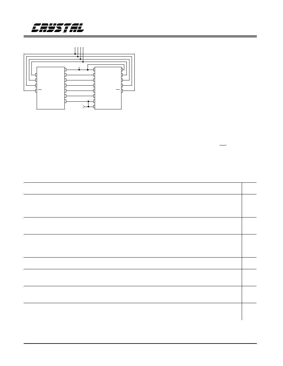
ACLKI
TCLK
RCLK
RPOS
RNEG
TPOS
TNEG
CS62180A/B
MODE
V+
TCLK
TPOS
TNEG
RNEG
RPOS
RCLK
SCLK
SDO
SDI
TO HOST CONTROLLER
CS61535A
CS61574A or CS61575
CS
SPS
SCLK
SDO
SDI
CS
1.544 MHz
CLOCK
SIGNAL
CLKE
Figure 3. Interfacing to a Crystal T1 LIU.
ADDR
(T) TRANSMIT
REGISTER NAME AND DESCRIPTION
(R) RECEIVE
0000
RSR
Receive Status Register - A read only register which reports all active receiver
alarm conditions.
R
0001
RIMR
Receive Interrupt Mask Register - A mask which allows selection of individual
alarm conditions for generation of hardware interrupt.
R
0010
BVCR
Bipolar Violation Count Register - A bipolar violation alarm is generated after
this 8 bit counter surpasses it's user definable limit.
R
0011
ECR
Error Count Register - Two separate 4 bit counters, which record OOF errors,
and frame bit or CRC errors. Like BVCR, each can be preset to a saturation
point.
R
0100
CCR
Common Control Register - Selects global configuration options, such as:
framing mode, zero suppression, or loopback.
T/R
0101
RCR
Receive Control Register - Selects receiver specific options, such as the resync
algorithm or insertion of digital milliwatt codes.
R
0110
TCR
Transmit Control Register - Selects transmitter specific options, such as alarm
generation, clear or idle channel enable, and external S-bit or CRC insertion.
T
0111
1000
1001
TIR1
TIR2
TIR3
Transmit Idle Registers - Each bit of the three TIR registers corresponds to an
individual DS0 channel. When set, that channel is replaced with an idle code.
T
1010
1011
1100
TTR1
TTR2
TTR3
Transmit Transparent Registers - Each bit corresponds to a DS0 channel. When
set, that signaling and B7 zero suppression is disabled for that channel.
T
1101
1110
1111
RMR1
RMR2
RMR3
Receive Mark Registers - Each bit corresponds to a DS0 channel. When set, the
channel data is replaced with an idle or digital milliwatt code.
R
Table 1. On-Chip Registers
CS62180A
CS62180B
DS225PP1
9

Common Control Register
The Common Control Register (CCR) deter-
mines global operating characteristics common
to both the transmitter and receiver. It currently
provides for selection of the framing mode
(193S, 193E, SLC-96
Æ
or T1DM), the format of
yellow alarms, the zero suppression format (B7
or B8ZS), loopback operation, and control of
output to RSR.2. In the CS62180A, CCR.7 is re-
served for future use, and should always be set 0
for proper operation. See Figure 4a for an over-
view of the CCR.
Loopback
CCR.0: LPBK
S e t t i n g L P B K (C C R . 0 ) t o "1 " p u t s t h e
CS62180A and CS62180B into loopback mode.
While in loopback, the TPOS/TNEG and TCLK
outputs are internally rerouted directly to the
RPOS/RNEG and RCLK inputs, while an un-
framed, all "1's" stream is output on the
TPOS/TNEG pins. All operating modes, except
blue alarm transmission, remain functional dur-
ing loopback. Note that enabling loopback will
usually invoke an out-of-frame (OOF) error un-
til the receiver can resync to the new framing
alignment. See the section on the Receive Con-
trol Register (RCR) for a description of the
resync options available.
Zero Suppression
CCR.1: B7
CCR.2: B8ZS
B7 and B8ZS select the zero suppression mode.
Setting B7 (CCR.1) to "1" will enable bit 7
zero substitution. This causes any channel word
with all zeros to be transmitted with bit 7 (2
nd
LSB) forced to a "1". B7 mode only affects the
transmitter, the receiver does not decode B7.
Note that bit 7 stuffing can be disabled on an
individual channel basis for clear channel trans-
mission via the Transmit Transparent Registers
TTR1 - TTR3 (see description of transmitter
which follows).
B8ZS coding operates independent of channel
boundaries, and is transparent to all other func-
tions. When using B8ZS, the final transmission
stream is examined before transmission, and
any eight consecutive zeros will be replaced
with a B8ZS code word before transmission.
CS62180A Only: If B8ZS (CCR.2) is set to a
"1", B8ZS zero substitution will be enabled in
both the transmitter and receiver. Incoming
B8ZS codes will be intercepted by the receiver
and replaced with 8 zeros before being proc-
essed by the rest of the receive side.
CS62180B Only: If B8ZS (CCR.2) is set to a
"1", B8ZS zero substitution will be enabled in
the transmitter. Independent of the setting of
CCR.2, any incoming B8ZS codes will be inter-
cepted by the receiver and replaced with 8
zeros before being processed by the rest of the
receive side. The receiver is always capable of
receving either AMI or B8ZS encoded data.
Note: For T1DM, CCR.1 and CCR.2 should be
set to a "0" since DDS
Æ
equipment assures a 1-
in-8 one's density.
7
(MSB)
6
5
4
3
2
1
0
(LSB)
FM1
FRSR2 EYELMD
FM
YELS
B8ZS
B7
LPBK
See Fig. 4b
0
B8ZS
0
FDL
See Fig. 4b
0
Bit 2
0
Disable
0 Transparent 0
Normal
1
COFA
1
Bit 2
1
S-bit
1
Enable
1 B7 Stuffing 1
Loopback
Figure 4a. Common Control Register (CCR)
CS62180A
CS62180B
10
DS225PP1

193S Yellow Alarm Format
CCR.3: YELS
The CS62180A and CS62180B supports two dif-
ferent yellow alarm formats for 193S framing.
Whichever format is selected, it will be used by
both the transmit side, for yellow alarm genera-
tion, and the receive side, for alarm detection.
When using 193S framing, a "0" in YELS
(CCR.3) will encode/decode yellow alarms as a
"0" in bit 2 (2
nd
MSB) of all channels. Setting
CCR.3 to "1" will cause yellow alarms to be en-
coded/decoded as a "1" is the S-bit position of
frame 12.
Note: For T1DM and SLC-96
Æ
, CCR.3 should
be set to a "0".
Framing Format
CCR.4: FM
CCR.7: FM1
As shown in Figure 4b, CCR.4 and CCR.7 select
the framing format. Note that in the CS62180A,
CCR.7 must be set to "0", and the SLC-96
Æ
and
T1DM formats are not available. See the text for
the Transmit Control Register (TCR) and Re-
ceive Control Register (RCR) for further
information on the particular options available
for each framing format.
Note: Changing the framing mode does not
force the receiver to resynchronize. A forced
resync should be done to insure correct receiver
synchronization after the framing mode is
changed.
193E Yellow Alarm Format
CCR.5: EYELMD
The CS62180A and CS62180B supports two dif-
ferent yellow alarm formats for 193E framing.
Whichever format is selected, it will be used by
both the transmit side, for yellow alarm genera-
tion, and the receive side, for alarm detection.
When using 193E framing, a "0" in EYELMD
(CCR.5) will encode/decode yellow alarms as a
repeating sequence of 00FF (hex) on the 4 kHz
facility data link (FDL). If CCR.5 is set, 193E
yellow alarms will be handled as a "0" in bit 2
(2
nd
MSB) of all channels.
Control of RSR.2
CCR.6: FRSR2
CCR.6 allows you to change the meaning of D2
in the Receive Status Register (RSR.2). If CCR.6
is clear, RSR.2 will report the detection of B8ZS
codes in the received T1 input. If CCR.6 is set to
a "1", RSR.2 will be used to signal a Change of
Frame Alignment (COFA). A COFA is reported
when the last receiver resync resulted in a
change of framing or multiframing alignment.
Refer to the description of the Receive Status
Register for further information.
7
4
FM1
FM
Format Selected
0
0
193S (D4)
0
1
193E (ESF)
1
0
SLC-96 (CS62180B only)
1
1
T1DM (CS62180B only)
Figure 4b. Framing Format Selection
CS62180A
CS62180B
DS225PP1
11

TRANSMITTER
The transmit sides of the CS62180A and
CS62180B have three types of inputs, the clock,
sync, and data inputs. Control is handled through
the serial port in host mode, and through the
mode control pins in hardware mode (see the last
section for a description of hardware mode op-
eration).
Input Data
None of the data inputs are buffered, so the data
at each input must be available at the appropriate
time for the CS62180A and CS62180B to multi-
plex into the output stream. All inputs are
sampled on the falling edge of TCLK. The delay
from input to output is 10 TCLK cycles.
NRZ data for DS0 channels is input on TSER.
Framing bits (F
T
or FPS bits) and CRC data may
either be generated internally or supplied by the
host system. If this data is to be externally sup-
plied, it must be inserted into the DS0 input
stream at the appropriate frames and input via
TSER.
S-bits may be generated internally, or externally
provided via TLINK. FDL bits are always pro-
v id e d ext e rna lly o n TLINK. B it-ro bbe d
signaling, when enabled, is always sampled at
TABCD. The CS62180A and CS62180B muxes
in data from these 3 sources (TSER, TLINK, and
TABCD) automatically depending on the trans-
mitter configuration.
Output Data
The completed T1 data stream, ready for line
transmission, is output on TPOS/TNEG. For op-
eration with a line interface which is transparent
to line coding, the output can be set to dual-
unipolar format by clearing bit 7 of the Transmit
Control Register (TCR.7). TCR.7 should be set
to a "1" for operation with a line interface which
provides AMI or B8ZS coding. In this configura-
tion, the data will be output on TPOS in NRZ
format, and TNEG will remain low. When oper-
ating in hardware mode, output defaults to the
dual-unipolar format. TPOS and TNEG may not
be tied together, so an external OR gate is rec-
ommended if NRZ output is required while in
hardware mode.
Frame/Multiframe Synchronization
The CS62180A and CS62180B maintain timing
for frame and multiframe alignment with internal
counters driven by TCLK. The timing signals
generated by those counters are output on
TCHCLK, TMO, TSIGSEL, TSIGFR, and
TLCLK. These counters determine when the
CS62180A and CS62180B will insert F-bits and
sample external signaling data. The frame and
multiframe counters can be reset independently
via TMSYNC and TFSYNC. If left to run with-
out a sync pulse, the CS62180A and CS62180B
will arbitrarily choose a framing alignment.
A low to high transition of TMSYNC, occurring
near the rising edge of TCLK, resets the
CS62180A's and CS62180B's counters to mark
the bit-period concurrent with the next falling
edge of TCLK as the F-bit of the first frame of a
new superframe. All other timing will be set to
match the superframe alignment automatically.
TMSYNC may be pulsed once at start-up and
left low, or left running in sync with superframe
timing.
A low to high transition of TFSYNC, occurring
near the rising edge of TCLK, resets the
CS62180A's and CS62180B's counters to mark
the bit-period concurrent with the next falling
edge of TCLK as the F-bit of a new frame. If
TMSYNC is used to set superframe alignment,
frame alignment will also be set, and TFSYNC
may be tied low. There is, of course, no harm in
using both TMSYNC and TFSYNC together, as
TFSYNC has no effect on multiframe alignment
if it is in sync. If, however, TFSYNC is used out
of sync with TMSYNC, the superframe align-
CS62180A
CS62180B
12
DS225PP1
ment will be moved forward by the least number
of bits necessary to be in alignment with the new
frame boundary.
Figure 5 shows the bit-level timing (with signal-
ling enabled). Note that the delay from input to
output is 10 TCLK cycles. TCHCLK transitions
high at the beginning of every DS0 channel
(50% duty cycle).
193S Timing
Frame and multiframe timing is output on
TCHCLK, TMO, TSIGSEL, TSIGFR, and
TLCLK. TMO transitions high at the beginning
of every superframe (50% duty cycle). TSIGFR
goes high during signaling frames (every 6
frames). TLCLK is a 4 kHz clock for the TLINK
input. TLCLK goes high during odd frames (ex-
ternal S-bit insertion).
TSIGSEL runs at twice the frequency of TMO.
Logical combination of TMO and TSIGSEL pro-
vides a way to distinguish the 6
th
and 12
th
frames for external multiplexing of signaling
channels. TMO is high for channel A, and low
for B. See Figure 6 for timing diagram.
193E Timing
Frame and multiframe timing is output on
TCHCLK, TMO, TSIGSEL, TSIGFR, and
TLCLK. TMO transitions high at the beginning
of every superframe (50% duty cycle). TSIGFR
goes high during signaling frames (every 6
frames). TLCLK is a 4 kHz clock for the TLINK
input. TLCLK goes high during odd frames
(FDL insertion).
TSIGSEL runs at twice the frequency of TMO.
Logical combination of TMO and TSIGSEL pro-
vides a way to distinguish the 6th, 12th, 18th,
and 24th frames for external multiplexing of sig-
naling channels. TMO is high for channels A
and B, and TSIGSEL is high for channels A and
C. See Figure 7 for timing diagram.
TCLK
TMSYNC
TFSYNC
TLINK
TSIGFR
TABCD
TSER
TCHCLK
10 TCLK Cycle Delay
TMO,
TSIGSEL,
TLCLK
TPOS,
TNEG
1
2
3
4
5
6
7
8
1
2
3
1
2
3
4
5
6
7
7
1
1
2
3
4
5
6
7
7
D
23
F
1
D
24
F
1
D
24
D
23
Figure 5. Bit Level Transmit Timing (193E, signaling enabled)
CS62180A
CS62180B
DS225PP1
13

SLC-96
Æ
Timing
Figure A6 of the Application Section, shows the
SLC-96
Æ
superframe structure. Note that in Fig-
ure A6, the first C bit (C1) resides in frame 12.
A low to high transition of TMSYNC identifies
Frame 1 of Figure A6.
Frame and multiframe timing is output on
TCHCLK, TMO, TSIGSEL, TSIGFR and
TLCLK. TSIGSEL can be used to identify the
location of the DL bits. The TSIGSEL output is
high during frames 58 to 11, and is low during
frames 12 to 57. When TSIGSEL is low, the
CS62180B accepts DL bits on TLINK at a 4
kHz rate, The DL bits which are input on
TLINK are: C1-C11, DC, DC, DC, M1-M3, A1,
A2, S1-S4. "DC" signifies "don't care" bits. The
DC-bit positions correspond to the spoiler bits.
The CS62180B internally generates the spoiler
bits. The data input on TLINK in the DC posi-
tion is ignored by the CS62180B. TLCLK is a 4
kHz clock for the TLINK input. TLCLK goes
high during odd frames.
TMO transitions high at the beginning of every
12th frame. TSIGFR goes high during signaling
frames (every 6 frames). The rising edge of
TMO identifies the 6
th
frame, and the falling
edge of TMO identifies the 12
th
frame for exter-
nal multiplexing of signaling channels. See
Figure 8 for timing diagram.
Frame
TMSYNC
TFSYNC
TMO
TSIGSEL
TSIGFR
TLCLK
X
2 3 4 5 6 7
1
8 9 10 11 12
2 3 4 5 6 7
1
8 9
14 15 16 17
19 20 21 22 23 24
13
18
A
B
C
D
A
Figure 7. 193E Multiframe Transmit Timing
Frame
TMSYNC
TFSYNC
TMO
TSIGSEL
TSIGFR
TLCLK
X
2 3 4 5 6 7
1
8 9 10 11 12
2 3 4 5 6 7
1
8 9 10 11 12
2 3 4 5 6 7
1
8 9
A
B
A
B
A
Figure 6. 193S Multiframe Transmit Timing
CS62180A
CS62180B
14
DS225PP1

T1DM Timing
Frame and multiframe timing is output on
TCHCLK, TMO, and TLCLK. TMO transitions
high at the beginning of every superframe (50%
duty cycle). TSIGFR goes high during signaling
frames (every 6 frames).
The channel 24 data link is input on TLINK us-
ing TLCLK. TLCLK is a 8 kHz clock with a
duty cycle of 1 bit period high per frame. When
TLCLK is high, TLINK will be sampled on the
falling edge of TCLK. See Figure 9 and
"Switching Characteristics - Transmitter" for tim-
ing diagrams.
TSIGSEL and TSIGFR serve no purpose in the
T1DM mode and can be ignored. However,
TSIGSEL and TSIGFR operate as in 193S
mode.
TMSYNC
TFSYNC
TMO
TSIGSEL
TSIGFR
TLCLK
A
B
A
B
Data Link
C1
C2
C3
C4
C5
C6
S4
M3
A1
S1
S2
S3
A2
Frame
X
12 13 14 15 16 17
11
18 19 20 21 22
56 57
72 1
55
2 3
44 45 46 47
49 50 51 52 53 54
48
B
58
Figure 8. SLC-96
Æ
Multiframe Transmit Timing
Frame
TMSYNC
TFSYNC
TMO
TSIGSEL
TSIGFR
TLCLK
X
2 3 4 5 6 7
1
8 9 10 11 12
2 3 4 5 6 7
1
8 9 10 11 12
2 3 4 5 6 7
1
8 9
Figure 9. T1DM Multiframe Transmit Timing
CS62180A
CS62180B
DS225PP1
15

Transmitter Control Register (TCR)
When in host mode, there are a number of op-
tions available for transmitter configuration
which can be enabled via the Transmit Control
Register (TCR), Transmit Transparent Registers
(TTR1 - TTR3), and Transmit Idle Registers
(TIR1 - TIR3). Serial read and write operations
to access these registers are explained in the Se-
rial Interface section above. When operating in
hardware mode, all control bits in the TCR de-
fault to "0" (except TCR.4, which defaults to "1"
to enable bit-robbed signaling), and dynamic
control is limited to the mode control pins as de-
scribed under hardware mode below.
The TCR provides control to enable bit-robbed
signaling, external framing bit, CRC, or S-bit in-
sertion, and yellow and blue alarm modes. It also
provides for two different idle code formats, and
selection of bipolar or NRZ output. Figure 10
shows an overview of the Transmit Control Reg-
ister.
Transmit Yellow Alarm
TCR.0: TYEL
Setting TYEL (TCR.0) to a "1" causes the
CS62180A and CS62180B to automatically gen-
erate and transmit a yellow alarm in the
appropriate format. In 193S mode the yellow
alarm format used will be determined by the set-
ting of CCR.3. In 193E mode, the yellow alarm
format will be determined by the setting of
CCR.5. See Common Control Register, above,
for description of the available yellow alarm for-
mats for 193S and 193E modes. In SLC-96
Æ
mode, the CS62180B does not generate the yel-
low alarm code. rather, the user transmits the
SLC-96
Æ
yellow alarm via the data link. In
T1DM mode, the yellow alarm is transmitted in
bit 5 of channel 24 (and CCR.3 should be set to
a "0"). Clearing TCR.0 disables yellow alarm
transmission.
Transmit Blue Alarm
TCR.1: TBL
Setting TBL (TCR.1) to a "1" generates a blue
alarm; an unframed sequence of all "1's". If a
framed, all "1's" signal is required, an FF (hex)
idle code may be output on all channels via ap-
propriate settings of TCR.3 and the TIR registers
(see Transmit Idle Code Select below). Blue
alarm (Alarm Indication Signal, or AIS) over-
rides all other transmission data, and a blue
alarm is automatically output during loopback.
Clearing TCR.1 disables blue alarm transmis-
sion.
193S, SLC-96
Æ
and T1DM S-bit Insertion
TCR.2: 193SI
TCR.2 is applicable to 193S, SLC-96
Æ
a nd
T1DM modes, but not to the 193E mode.
In the 193S and T1DM modes, setting 193SI
(TCR.2) to a "1" allows the S-bit (all even F-
bits) to be externally supplied via TLINK. When
TCR.2 is clear, the S-bit will be internally gen-
erated.
In the SLC-96
Æ
mode, setting 193SI (TCR.2) to
a "1" allows the S-bit (selected even F-bits) to be
externally supplied via TLINK, and the user
must input all Fs, spoiler and DL bits. When
TCR.2 is clear, the CS62180B generates the
SLC-96
Æ
spoiler bits and Fs bits, and the user
7
(MSB)
6
5
4
3
2
1
0
(LSB)
ODF
TFPT
TCP
RBSE
TIS
193SI
TBL
TYEL
0
Bipolar
0
Internal
0
Internal
0
Disabled
0
7F (Hex)
0
Internal
0
Normal
0
Normal
1
NRZ
1
External
1
External
1
Enabled
1
FF (Hex)
1
External
1 Blue Alarm 1
Yel. Alarm
Figure10. Transmit Control Register (TCR)
CS62180A
CS62180B
16
DS225PP1

inputs all other DL bits on TLINK using
TLCLK.
Note: When using internal S-bit generation
(TCR.2 = 0) in conjunction with external F
T
bit
insertion (TCR.6 = 1), the CS62180A and
CS62180B will logically 'OR' the value at TSER
with the internally generated value. This means
that the data on TSER during S-bit periods
should always be "0" to avoid corrupting the
generated F
S
pattern.
Transmit Idle Code Select
TCR.3: TIS
Individual DS0 channels can be replaced with
idle codes by setting the corresponding bits in
the Transmit Idle Registers (TIR1 - TIR3) de-
scribed below. TIS (TCR.3) selects which of two
codes to use. A "0" in TCR.3 will cause a 7F
(hex) to be inserted into the channels specified in
the TIR. Setting TCR.3 to a "1" will select an FF
(hex) code. By asserting all 24 channels idle in
the TIR, this setting can be used to generate a
"framed" blue alarm. Whichever mode is se-
lected, bit-robbed signaling will still effect idle
channels unless they are programmed clear (see
Transmit Transparent Registers, below).
Robbed Bit Signaling Enable
TCR.4: RBSE
A "0" in RBSE (TCR.4) will disable bit-robbed
signaling. Setting TCR.4 to a "1" will enable sig-
naling in all channels. In this mode, data on
TABCD is inserted into the LSB of all DS0
channels during signaling frames. For mixed
voice and data transmission, individual DS0
channels can be programmed clear by setting the
corresponding bits in the Transmit Transparent
Registers (TTR1 - TTR3) described below.
CRC Pass-through
TCR.5: TCP
In 193E framing mode, the CRC bits (F-bit of
frames 2, 6, 10, 14, 18, and 22) may be either
generated internally, or supplied by the user.
Clearing TCP (TCR.5) causes the CS62180A
and CS62180B to generate and insert the CRC
bits automatically. If TCR.5 is set to a "1", data
for the CRC channel may be externally supplied.
When using this mode, CRC bits are sampled
from TSER, and must be externally multiplexed
into the DS0 channel data at the F-bit times of
CRC frames.
F
T
/FPS Pass Through
TCR.6: TFPT
When TFPT (TCR.6) is clear, the framing bits
for 193S, T1DM and SLC-96
Æ
(F
T
), or 193E
(FPS) are generated internally and automatically
inserted into the outgoing data stream. Setting
TCR.6 to a "1" allows the framing bits to be ex-
ternally provided. When using this mode,
framing bits are sampled from TSER, and must
be externally multiplexed into the DS0 channel
data at the F-bit times of the appropriate frames.
See note under TCR.2, above.
Output Data Format
TCR.7: ODF
ODF (TCR.7) allows the format of the output
data at TPOS/TNEG to be set to either dual-
unipolar or NRZ format. Clearing TCR.7 selects
for dual-unipolar format on TPOS/TNEG. Set-
ting TCR.7 to a "1" causes data to be output on
TPOS in NRZ format, and TNEG is held low.
When operating in hardware mode, output de-
faults to the dual-unipolar format. TPOS and
TNEG may not be tied together, so an external
OR gate is recommended if NRZ is required
while in hardware mode.
CS62180A
CS62180B
DS225PP1
17

Transmit Transparent Registers (TTR)
The Transmit Transparent Registers allow indi-
vidual DS0 channels to be programmed clear,
disabling robbed bit signaling and B7 zero sup-
pression for that channel (if selected, B8ZS is
unaffected by transparent channels). There are 3
TTR registers: TTR1, TTR2, and TTR3. Each bit
in the TTR registers corresponds to a DS0 chan-
nel: TTR1.0 = channel 1, TTR1.7 = channel 8,
TTR2.7 = channel 16, etc. A channel is pro-
gra mmed cl ear b y sett ing the bit whic h
corresponds to that channel in the appropriate
TTR register. See Figure 11.
Transmit Idle Registers (TIR)
By setting the appropriate bits in the Transmit
Idle Registers, individual DS0 channels can be
replaced with the idle code selected via TCR.3
(see above). If the idle channel is not also pro-
grammed clear (via TTR1 - TTR3), the code
may be corrupted during signaling frames if
robbed bit signaling is enabled (TCR.4 = 1).
There are 3 TIR registers: TIR1, TIR2, and
TIR3. Each bit in the TIR registers corresponds
to a DS0 channel: TIR1.0 = channel 1, TIR1.7 =
channel 8, TIR2.7 = channel 16, etc. A channel
is programmed idle by setting the bit which cor-
responds to that channel in the appropriate TIR
register. See Figure 12.
Transmission Insertion Hierarchy
Figures 13a - 13c give an overview of the deci-
sion hierarchy which determines the final
composition of the output stream. It shows the
various control options as inputs into decision
branches of the flow chart, and the order in
which the various optional signals are muxed
into the final data stream.
7
(MSB)
6
5
4
3
2
1
0
(LSB)
TIR1
CH8
CH7
CH6
CH5
CH4
CH3
CH2
CH1
TIR2
CH16
CH15
CH14
CH13
CH12
CH11
CH10
CH9
TIR3
CH24
CH23
CH22
CH21
CH20
CH19
CH18
CH17
"0" = Normal
"1" = Corresponding DS0 Channel is Replaced with Idle Code. (See TCR.3)
Figure 12. Transmit Idle Registers (TIR1 - TIR3)
7
(MSB)
6
5
4
3
2
1
0
(LSB)
TTR1
CH8
CH7
CH6
CH5
CH4
CH3
CH2
CH1
TTR2
CH16
CH15
CH14
CH13
CH12
CH11
CH10
CH9
TTR3
CH24
CH23
CH22
CH21
CH20
CH19
CH18
CH17
"0" = Normal
"1" = Corresponding DS0 Channel is Transparent. (Not signaling or B7 Insertion.)
Figure11. Transmit Transparent Registers (TTR1 - TTR3)
CS62180A
CS62180B
18
DS225PP1
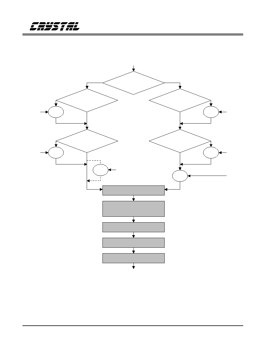
F-bit Insertion
Framing Mode
193S, SLC-96 , T1DM
TSER
193E
TLINK
TSER
TLINK
F
T
F
S
TCR.6
F Passthrough
T
TCR.6
FPS Passthrough
0 = Internal
1 = External
0 = Internal
1 = External
TCR.5
CRC Passthrough
TCR.2
S-bit Insertion
0 = Internal
1 = External
TSER
0 = Internal
1 = External
TSER
FDL
FPS
CRC
Robbed Bit Signaling &
B7 Zero Suppression
Idle Code Insertion
Yellow Alarm Insertion
B8ZS Zero Suppression
Blue Alarm or Loopback
TPOS/TNEG
TLINK
F
S
SLC-96
DL bits
Æ
Æ
Figure 13a. Transmit Insertion Hierarchy: Framing Bits
CS62180A
CS62180B
DS225PP1
19
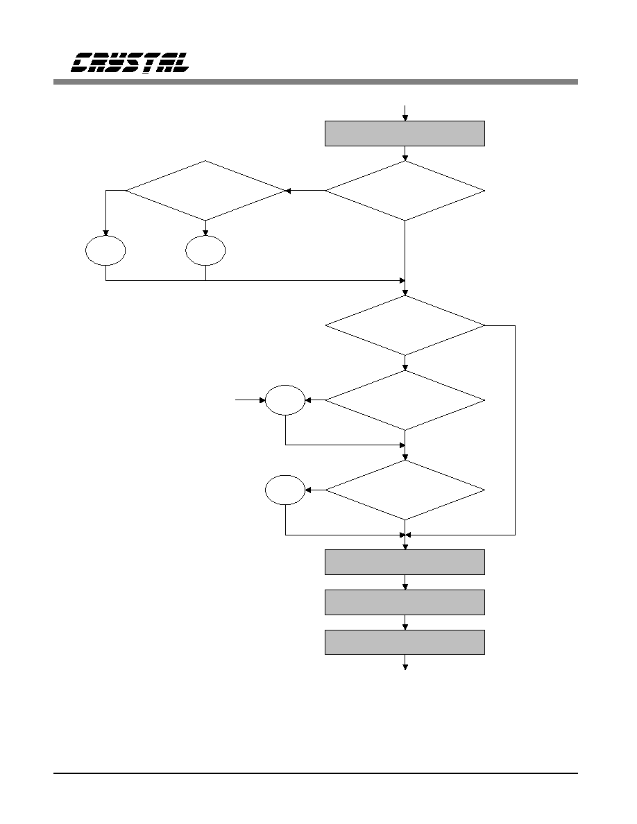
TABCD
TTR
Transparent Channels?
TCR.4
Robbed Bit
Signaling?
CCR.1
B7 Zero Suppression
TSER
1 = Idle
0 = Normal
FF
7F
1
0
1 = Transparent
0 = Normal
1 = Signaling
0 = Disabled
b
8
1 = B7
0 = Disabled
B7
Idle Code Insertion
Robbed Bit Signaling &
B& Zero Suppression
TIR
Idle Channels?
TCR.3
Idle Code
F-bit Insertion
Yellow Alarm Insertion
B8ZS Zero Suppression
Blue Alarm or Loopback
TPOS/TNEG
Figure 13b. Transmit Insertion Hierarchy: Idle Codes, Signaling, and B7
CS62180A
CS62180B
20
DS225PP1

CCR.5
Alarm Format
193E
CCR.3
Alarm Format
193S
CCR.0
Loopback?
CCR.2
B8ZS Zero Suppression?
TCR.1
Blue Alarm?
TSER
1 = Yes
0 = No
B8ZS
BLUE
BLUE
1
0
1
0
FDL
TPOS/TNEG
B8ZS Zero Suppression
Yellow Alarm Insertion
F-bit Insertion
Blue Alarm
Robbed Bit Signaling &
B7 Zero Suppresion
1 = Yes
1 = Yes
0 = No
0 = No
Loopback
Idle Code Insertion
TCR.0
Yellow Alarm?
1 = Yes
0 = No
193S
193E
T1DM
SLC-96
DL
TLINK
S
12
b
2
C
24
b
2
Æ
Figure 13c. Transmit Insertion Hierarchy: Alarms, B8ZS, and Loopback
CS62180A
CS62180B
DS225PP1
21

RECEIVER
The receive sides of the CS62180A and CS62180B
have only three inputs: the clock (RCLK), the in-
coming signal (RPOS/RNEG), and a reset pin
(RST). The receiver determines the framing syn-
chronization of the incoming data, and outputs the
timing information on the six timing clocks:
RLCLK, RCHCLK, RFSYNC, RMSYNC,
RSIGFR, and RSIGSEL. Alarms and error condi-
tions are recorded in the Receive Status Register,
and output in real time on the five status pins:
RYEL, RCL, RBV, RFER, and RLOS. The de-
coded data is separated into it's component
channel, link, and signaling components and output
on RSER, RLINK, and RABCD respectively.
When in host mode, the Receive Control Register
allows control of the sync algorithm, and insertion
of idle or digital milliwatt (
µ
-LAW) codes into in-
dividual DS0 channels. The internal error counters
can be accessed, and the Interrupt Mask Register
can be programmed to specify the conditions under
which a hardware interrupt is generated on INT.
When running in hardware mode, receiver status
can still be monitored on the status pins; and access
to the error counters, sync algorithm, interrupt
mask, and the insertion of idle codes are disabled.
Input Data
The receiver accepts the incoming T1 stream via
RPOS/RNEG in dual-unipolar format. Tying
RPOS/RNEG together disables the bipolar viola-
tion alarm and allows reception of data in NRZ
format. Input data is sampled on the falling edge of
RCLK. Delay from input at RPOS/RNEG to out-
put on RSER is 13 RCLK periods.
Output Data
The receiver will attempt to sync and decode the
framing format selected via CCR.4 and CCR.7.
The decoded T1 stream is output in NRZ format on
RSER, and updated every RCLK period. Output
data is latched on the rising edge of RCLK, and
held until the next update.
Link and signaling data is always output on
RLINK and RABCD respectively, independent of
the transmitter configuration. RABCD outputs the
LSB of every DS0 channel word, whether it is cur-
rently a signaling frame or not. The data is updated
on the channel boundary, concurrent with the MSB,
and held until the next update (8 or 9 bits). RLINK
outputs either S-bit, SLC-96
Æ
DL or FDL bits,
depending on the framing format. Data is up-
dated 1 bit period prior to the F
S
or FDL frame
and held until the next update (2 frames).
Output Clocks
Several timing clocks are provided for identify-
ing this data. The timing clocks are RLCLK,
RCHCLK, RFSYNC, RMSYNC, RSIGFR, and
RSIGSEL. Logical combination of these six sig-
nals allows easy extraction of any part of the
received data stream. RMSYNC runs on a 50%
duty cycle, and transitions high at the start of
each new superframe output on RSER. RFSYNC
transitions high at the start of every new frame.
Individual DS0 channels are identified by
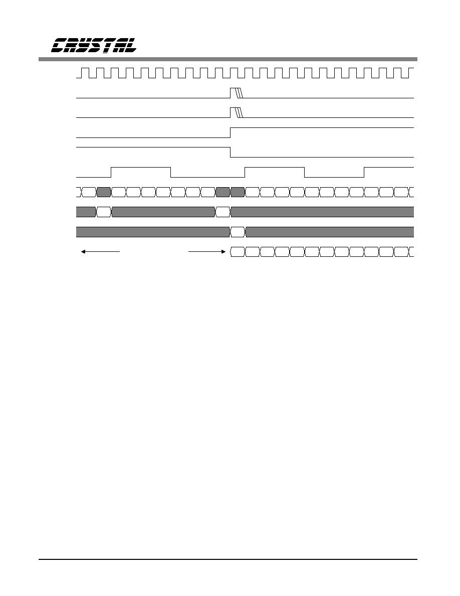
RCHCLK, which runs on a 50% duty cycle and
transitions high at the MSB of every individual
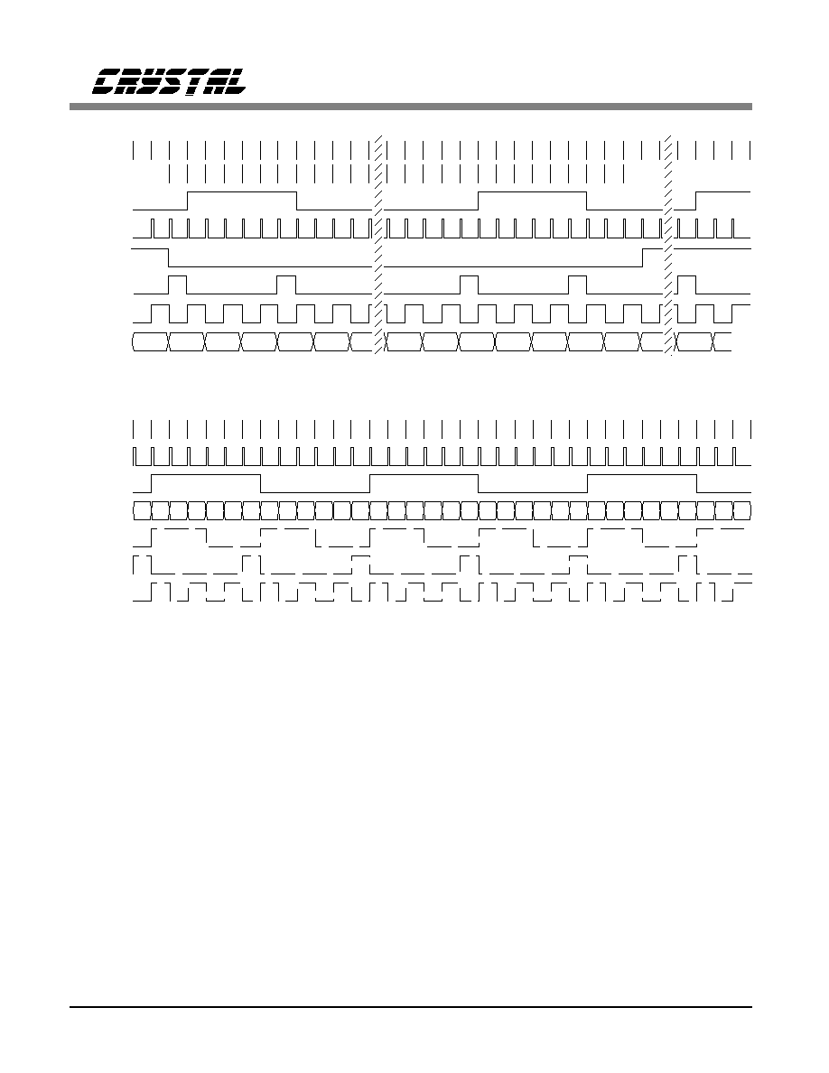
time slot. Bit level timing is shown in Figure 14.
193S Timing
Link data can be identified by RLCLK, which
goes high for all odd numbered frames. RSIGFR
is high for signaling frames, and low at all other
times. RSIGSEL runs at twice the frequency of
RMSYNC. Logical combination of RMSYNC
and RSIGSEL provides a way to distinguish the
6
th
and 12
th
frames for external multiplexing of
signaling channels. RMSYNC is high for those
frames containing A signaling bits, and low for
frames containing B bits. Refer to Figure 15 for
a timing diagram.
CS62180A
CS62180B
22
DS225PP1

Frame
RMSYNC
RFSYNC
RSIGSEL
RSIGFR
RLCLK
RLINK
12
2 3 4 5 6 7
1
8 9 10 11 12
2 3 4 5 6 7
1
8 9 10 11 12
2 3 4 5 6 7
1
8 9
B
A
A
B
A
B
S
2
S
4
S
12
S
6
S
8
S
10
S
2
S
4
S
12
S
6
S
8
S
10
S
2
S
4
S
12
S
6
S
8
Figure 15. 193S Multiframe Receive Timing
Frame
RMSYNC
RFSYNC
RSIGSEL
RSIGFR
RLCLK
RLINK
D
A
B
C
A
D
24
2 3 4 5 6 7
1
8 9 10 11 12
2 3 4 5 6 7
1
8 9
14 15 16 17
19 20 21 22 23 24
13
18
F
1
F
3
F
5
F
7
F
9
F
11
F
13
F
15
F
17
F
19
F
21
F
23
F
1
F
3
F
5
F
7
Figure 16. 193E Multiframe Receive Timing
RCLK
RFSYNC
RLINK
RSIGFR
RABCD
RSER
RCHCLK
RMSYNC,
RSIGSEL,
RLCLK
Channel 1 LSB
RPOS,
RNEG
1
2
3
4
5
6
7
8
1
2
3
4
5
6
7
8
1
2
3
4
1
2
3
4
5
6
7
1
2
3
4
5
6
7
3
4
5
6
7
23
F
1
F
24
D
23
D
23
D
24
D
1
F
24
D
1
F
Figure 14. Bit Level Receive Timing (193E mode)
CS62180A
CS62180B
DS225PP1
23
193E Timing
Link data can be identified by RLCLK, which
goes high for all odd numbered frames. RSIGFR
is high for signaling frames, and low at all other
times. RSIGSEL runs at twice the frequency of
RMSYNC. Logical combination of RMSYNC
and RSIGSEL provides a way to distinguish the
6
th
, 12
th
, 18
th
, and 24
th
frames for external mul-
tiplexing of signaling channels. RMSYNC is
high for frames containing A and B signaling
bits, and RSIGSEL is high for frames with A
and C bits. Refer to Figure 16 for a timing dia-
gram.
SLC-96
Æ
Timing
The CS62180B will output 36 bits of the DL on
RLINK using RLCLK. RSIGSEL can be used to
locate the DL bits. RSIGSEL will be held high
in those frames where Fs bits and the last spoiler
bit are present (frames 58 to 11). RSIGSEL is
held low in all other frames (frames 12 to 57).
RSIGFR is high for signaling frames, and low at
all other times. RMSYNC is high for frames
containing A signaling bits, and low for frames
containg B bits. Refer to Figure 17 for a timing
diagram. In SLC-96
Æ
mode, the start of a new
multiframe occurs on the second rising edge of
RMSYNC which occurs while RSIGSEL is high.
A multiframe synchronization signal can be gen-
erated from RMSYNC and RSIGSEL using the
Frame
RFSYNC
12
2 3 4 5 6 7
1
8 9 10 11 12
2 3 4 5 6 7
1
8 9 10 11 12
2 3 4 5 6 7
1
8 9
RLINK
RLCLK
RSIGFR
RSIGSEL
RMSYNC
Figure 18. T1DM Multiframe Receive Timing
RMSYNC
RFSYNC
Data Link
C1
C2
C3
C4
C5
C6
S4
M3
A1
S1
S2
S3
A2
Frame
X
12 13 14 15 16 17
11
18 19 20 21 22
56 57 58
72 1
55
2 3
44 45 46 47
49 50 51 52 53 54
48
RLINK
RSIGSEL
RSIGFR
A
B
A
B
B
RLCLK
C1
C2
C3
C4
C5
C6
M3
A1
A2
S1
S2
S3
S4
F
S
F
S
F
S
Figure 17. SLC-96
Æ
Multiframe Receive Timing
CS62180A
CS62180B
24
DS225PP1

circuit shown in Figure A1 in the Applications
section.
T1DM Timing
The 8 kHz link data can be sampled on RLINK
using the falling edge of RFSYNC. Refer to Fig-
ure 18 and "Switching Characteristics≠Receiver"
for timing diagrams. RSIGFR, RSIGSEL and
RLCLK serve no purpose in the T1DM mode
and may be ignored.
Receive Control Register (RCR)
The RCR provides for insertion of either idle or
digital milliwatt codes, and has six different con-
trol bits which enable a large number of options
for tailoring the receiver resync behavior. Refer
to Figure 19 for an overview of the RCR.
Receive Code Select/Insert
RCR.4: RCS
RCR.5: RCI
When enabled via RCI (RCR.5), the Receive
Mark Registers are used to select individual DS0
channels for insertion of idle or digital milliwatt
codes, as selected via RCS (RCR.4). There are
three RMR registers: RMR1, RMR2, and RMR3
(Figure 20). Each bit in the RMR registers corre-
sponds to a received DS0 channel: RMR1.0 =
channel 1, RMR1.7 = channel 8, RMR2.7 =
channel 16, etc. A channel is marked for code
insertion by setting the bit which corresponds to
that channel in the appropriate RMR register.
When RCR.5 is clear, code insertion is disabled,
and the contents of the RMR registers are ig-
nored.
RCS (RCR.4) selects whether to insert an idle
code, or a digital milliwatt code, into the individ-
ual DS0 channels marked in the three Receive
Mark Registers (RMR1 - RMR3). Clearing
RCR.4 will select for an idle code (7F hex) to be
inserted into marked channels. Setting RCR.4 to
a "1" will cause a digital milliwatt code (
µ
-LAW
format) to be inserted into all marked channels.
Receiver Synchronization
The receiver monitors the incoming signal for
loss of frame alignment (based on F
T
or FPS bits
only). Unless auto resync has been disabled via
RCR.1 (see below), the receiver will automat-
ically initiate a search for the correct framing
alignment when loss of synchronization is de-
tected, and RLOS (pin 39) will go high until a
new framing alignment is declared.
7
(MSB)
6
5
4
3
2
1
0
(LSB)
RMR1
CH8
CH7
CH6
CH5
CH4
CH3
CH2
CH1
RMR2
CH16
CH15
CH14
CH13
CH12
CH11
CH10
CH9
RMR3
CH24
CH23
CH22
CH21
CH20
CH19
CH18
CH17
"0" = Normal
"1" = Corresponding DS0 Channel is Replaced with Idle or Digital Milliwatt Code. (See RCR.4 and RCR.5)
Figure 20. Receive Mark Registers (RMR1 - RMR3)
7
(MSB)
6
5
4
3
2
1
0
(LSB)
ARC
OOF
RCI
RCS
SYNCC
SYNCT
SYNCE RESYNC
0
OOF/RCL
0
2 out of 4
0
Disabled
0
Idle (7F)
0 Ft/FPS only 0
10 bits
0 Autoresync
rising edge
triggered.
1
OOF only
1
2 out of 5
1
Enabled
1
Milliwatt
1
Fs/CRC
1
24 bits
1
Disabled
Figure 19. Receive Control Register (RCR)
CS62180A
CS62180B
DS225PP1
25

When the receiver initiates an auto resync,
RSIGFR is held low, but all other output timing
will continue in the old alignment until the new
framing is found. When the new framing align-
ment is qualified, the output timing will change
to the new alignment at the beginning of the next
superframe (or at the start of frame 13 in SLC-
96
Æ
mode), and RLOS will return low one bit
period before the F-bit of the second frame.
A receiver resync has no effect on the transmit
side timing or configuration, and behavior of the
output timing and RLOS pin is the same as that
for an auto resync described above. This is in
contrast to a reset initiated via the RST pin,
which clears all internal registers on the falling
edge, including the transmit side registers, resets
the output timing while RST is low, and then in-
itiates a receiver resync on the rising edge.
The time it takes the receiver to resync depends
on resync algorithm selected via RCR.2 and
RCR.3. The remaining bits in the RCR (1, 6, and
7) determine under what conditions an automatic
resync will be initiated.
Forced Resync
RCR.0: RESYNC
RESYNC (RCR.0) can be used to force a re-
ceiver resync. Toggling RCR.0 will initiate a
resync immediately on the rising edge. It must
then be cleared and set again to initiate another
resync. Toggling RCR.0 when going into loop-
back mode will force the receiver to resync to
the new frame alignment immediately. This is
faster than waiting for the internal hardware to
recognize an out-of-frame (OOF) condition and
initiating an automatic resync.
Note: A forced resync should be issued after a
change in framing mode to insure correct syn-
chronization.
Auto Resync Conditions
RCR.1: SYNCE
RCR.6: OOF
RCR.7: ARC
SYNCE (RCR.1) can be set to a "1" to com-
pletely disable automatic resync. If RCR.1 is
clear, a resync will automatically be initiated
when the conditions specified by RCR.6 and
RCR.7 are detected.
OOF (RCR.6) specifies how many framing bits
(F
T
or FPS channels only) must be in error be-
fore the receiver declares an out-of-frame (OOF)
condition. A resync is always initiated (unless
disabled) when an OOF is detected. If RCR.6 is
clear, an OOF is declared if 2 out of 4 F
T
or FPS
bits are in error. If RCR.6 is set to a one, an
OOF is declared if 2 out of 5 framing bits are
errored. Note that the setting of RCR.6 also ef-
fects the reporting of OOF events to the Receive
Status Register (RSR) and Error Count Register
(ECR). Refer to the appropriate sections below
for details.
ARC (RCR.7) declares whether the receiver will
initiate a resync on an OOF event only, or resync
on both OOF and carrier loss (RCL). If RCR.7 is
cleared, the receiver will commence resync upon
detection of either an OOF event (as defined by
RCR.6 above), or an RCL. If RCR.7 is set, the
receiver will only resync in response to an OOF
condition.
Resync Algorithm
RCR.2: SYNCT
RCR.3: SYNCC
SYNCT (RCR.2) allows you to declare how
many bits must be qualified in the framing pat-
tern before the receiver declares synchronization.
When RCR.2 is clear, 10 consecutive F
T
or FPS
framing bits preceding an RMSYNC rising edge
must be qualified. Setting RCR.2 to a "1" re-
quires the CS62180A and CS62180B to qualify
24 consecutive F
T
or FPS bits preceding an
CS62180A
CS62180B
26
DS225PP1

RMSYNC rising edge before declaring synchro-
nization.
SYNCC (RCR.3) allows you to modify the algo-
rithm employed to search for and qualify the
framing alignment. There are two different quali-
fying conditions available for each framing
mode, and the meaning of RCR.3 depends on
which framing mode has been selected via
CCR.4.
193S Resync
When operating with the 193S framing format,
RCR.3 selects whether or not the CS62180A and
CS62180B will qualify the F
S
bits during resync.
If a non-standard S-bit pattern is being used,
clearing RCR.3 will enable the device to first
search for the F
T
framing pattern to find frame
alignment, and then only reset multiframe align-
ment if the F
S
pattern can be found. This means
that if a valid F
S
pattern is not found, synchroni-
za tio n wi ll be declared anyway, and the
multiframe alignment indicated by RMSYNC
may be false. The S-bits output on RLINK can
be used to decode framing externally in such ap-
plications.
When using standard F
S
signaling, setting
RCR.3 to a "1" will cause the device to cross
check the F
T
and F
S
patterns to find sync, and
both patterns must be valid before sync is de-
clared. Synchronization will be declared after the
number of F
T
bits selected by RCR.2 separated
by valid F
S
bits have been qualified. Note that
in either setting, S-bit format yellow alarms are
recognized by the synchronizer if they have been
selected by setting CCR.3.
193E Resync
Clearing RCR.3 while in 193E mode will cause
the CS62180A and CS62180B to use only the
FPS framing pattern when looking for a valid
framing alignment. If RCR.3 is set, the device
will attempt to qualify the CRC bits after a can-
didate alignment has been found. If the CRC
codes match, then the new alignment will be de-
clared, if not, the device will try two more times.
If the third CRC code does not qualify, then the
device will start a new resync procedure and
continue in this manner until a framing align-
ment can be verified with the CRC codes.
Note that after 24 ms, if there are still multiple
candidates for framing alignment, the device will
test the CRC codes to eliminate false candidates
regardless of the setting of RCR.3. After the
framing alignment has been found, it takes about
9 ms for the device to check the CRC codes for
the first superframe. If that superframe fails, it
takes about 3 ms to check each additional CRC
code.
SLC-96
Æ
Resync
When operating with the SLC-96
Æ
framing for-
mat, the receiver should be programmed for
F
S
/F
T
cross-coupling (RCR.3=1) and for mini-
mum resync time (RCR.2=0). This causes the
CS62180B to sync on the 10 valid F
T
bits
seprated by valid Fs bits in frames 65 through
11, and prevents false synchronization to data
link and/or spoiler bits.
Note: The CS62180B does not check SLC-96
Æ
multiframe alignment once synchronization is
declared. In applications such as test equipment
where the input data framing format may change
or the multiframe alignment may change when
the frame alignment does not, the datalink proc-
essor should check the phase between RSIGSEL
and the DL spoiler bits on RLINK and issue a
forced resync when multiframe alignment is in-
correct. In the SLC-96
Æ
applications, a forced
resync should be issued after the device is con-
figured. Since the CS62180B defaults to the
193S framing mode at power up it may sync to
SLC-96
Æ
data while in the 193S mode. If this
occurs the multiframe alignment may be incor-
rect after the CS62180B is programmed for
SLC-96
Æ
mode even though the frame alignment
CS62180A
CS62180B
DS225PP1
27

is correct. Since the frame alignment is correct
no OOF event or auto resync occurs. A forced
resync will force the 62180B to synchronize to
the frame and multiframe alignment.
T1DM Resync
Resync is based upon the 6-bit sync word in
channel 24. Once the sync word is recognized,
6 consecutive frames with the correct sync word
and F
S
/F
T
bits are required before declaring syn-
chronization. RCR.2 must be set to "0". RCR.3
is ignored. When frame synchronization is de-
clared, RLOS goes low and RFSYNC is output
concurrent with the f-bits. However, the super-
frame output clocks (RMSYNC, RSIGFR and
RSIGSEL) are held low for an additional short
period of time until superframe synchronization
is found.
Receive Status Register (RSR)
The CS62180A and CS62180B monitors the in-
coming T1 data for a number of error conditions.
These alarms are recorded in the Receive Status
Register (RSR), and output in real time on the
status pins: RYEL, RCL, RBV, RFER, and
RLOS. Three presettable counters are provided
which count the number of occurrences of Bipo-
lar Violations, Framing and CRC errors. The
Receive Interrupt Mask Register, RIMR, can be
set to specify which of the eight errors recorded
in the RSR will generate a hardware interrupt on
INT. When operating in hardware mode, all
these registers are cleared, and only the status
pins provide real time alarm information.
F
"0" "0" "0" "1"
Resync
F
Loss of Carrier
(32nd or 128th "0")
Resync
F
OOF
Loss of Carrier (RCL)
Bipolar Violation
CRC Error
RCLK
RSER
RMSYNC
RFSYNC
RFER
RBV
RCL
RLOS
Reframed
Errored F-bit
2nd Frame
Bipolar Violation
Figure 22. Receive Status Pin Timing
7
(MSB)
6
5
4
3
2
1
0
(LSB)
BVCS
ECS
RYEL
RCL
FERR
B8ZSD
RBL
RLOS
1 =
BVCR
Saturation
ECR
Saturation
Yellow Alarm
Detected
Carrier Loss
Detected
Frame Error
Detected
B8ZS/COFA
Detected
Blue Alarm
Detected
Resync in
progress
Figure 21. Receive Status Register (RSR)
CS62180A
CS62180B
28
DS225PP1

Each of the eight bits of the RSR (Figure 21)
corresponds to an alarm condition. A bit in the
RSR is set when the corresponding alarm is de-
tected. It will be cleared by a direct read (a burst
read will have no effect) of the RSR, unless the
alarm condition persists (see Alarm Servicing,
below). TCLK is used to clock the internal cir-
cuitry which clears RSR after it is directly read;
therefore, a 1.544 MHz signal must always be
input to TCLK, even for a "receiver-only" appli-
cation. The status pins which correspond to
many of the RSR bits operate in real time. They
go high when the error is detected, and return
low either immediately, or as soon as the error
condition is cleared. Alarms are reported syn-
chronously with the emergence of the offending
bits on RSER. See Figure 22, and the corre-
sponding alarm description below for further
description of status pin timing.
Receive Loss of Sync
RSR.0: RLOS
RLOS (RSR.0) goes high when a receiver resync
is in progress. When the receiver is set to auto
resync (RCR.1 = 0), the receiver will commence
resync when an OOF event or loss of carrier is
detected. If in response to an OOF, RLOS transi-
tions high synchronously with the output of the
offending F-bit on RSER (see RCR.6).
CS62180A only: If in response to an RCL,
RLOS goes high with the 32
nd
consecutive zero
bit.
CS62180B only: If in response to an RCL,
RLOS goes high with the 128th
±
1 consecutive
zero bit.
The RLOS pin will return low one bit period
prior to the F-bit of the second frame after the
new alignment has been declared (timing signals
will reset at the start of the new superframe). Re-
fer to Receiver Synchronization, above, for more
information.
Receive Blue Alarm
RSR.1: RBL
RBL (RSR.1) will transition high when a blue
alarm is detected, and is updated at the begin-
ning of odd-numbered frames.
CS62180A only: A blue alarm is reported when-
ever less than 3 zeros are detected in the channel
data of 2 consecutive frames (F-bit positions are
not tested). There is no status pin corresponding
to RBL.
CS62180B only: A blue alarm is reported when-
ever unframed all ones occurs, as per Bellcore
TR-TSY-000191. The algorithm used is to simul-
taneously check for an out-of-frame (OOF)
condition, and check for 14 or less zeros out of
13,895 bits. All bits, including frame bits, are
tested. RBL goes high on a frame boundary.
RBL goes low immediately (indicating the termi-
nation of the AIS condition) if OOF goes low, or
if 15 or more zeros are counted and the number
of bit periods is less than or equal to 13,895.
RBL is reported on pin 3 of the 44-pin PLCC
package. There is no status pin corresponding to
RBL on the 40-pin DIP package.
B8ZS/COFA Detect
RSR.2: B8ZSD
B8ZSD (RSR.2) is a multifunction bit. It can be
configured either to report the detection of B8ZS
codes, or to indicate a change of framing align-
ment. This selection is performed through the
setting of CCR.6 (see Common Control Register,
above). There is no status pin corresponding to
RSR.2.
If CCR.6 is clear, RSR.2 will go high every time
a B8ZS code is detected in the incoming T1
data. This detector remains operational, whether
or not B8ZS substitution has been enabled via
CCR.2.
CS62180A
CS62180B
DS225PP1
29

If CCR.6 is set to a "1", RSR.2 will go high in
response to a Change of Frame Alignment
(COFA). A COFA is reported when the last re-
ceiver resync resulted in a change of frame or
multiframe alignment. RSR.2 will go high at the
same time the timing signals are reset after a
resync. (See Receiver Synchronization, above.)
Frame Bit Error
RSR.3: FERR
FERR (RSR.3) is set whenever a framing bit is
in error.
193S Frame Bit Errors: The framing bits for the
193S is the F
T
channel (odd F-bits). The RFER
status pin (pin 38) signals the same F
T
errors,
but in addition, signals F
S
errors as well. When
signaling a frame bit error, RFER will go high
simultaneously with the output of the offending
F-bit on RSER, and hold for 2 bit periods.
193E Frame Bit Errors: The framing bits for the
193E mode are the FPS channel (F-bits of
frames 4, 8, 12, 16, 20, and 24). The RFER
status pin (pin 38) signals the same FPS errors,
but in addition, signals CRC errors as well.
When signaling a frame bit error, RFER will go
high simultaneously with the output of the of-
fending F-bit on RSER, and hold for 2 bit
periods. When signaling a CRC error, RFER will
transition high 1/2 bit before the new superframe
to indicate a CRC error in the previous super-
frame. It goes high on the falling edge of RCLK,
and is held for only one period, returning low on
the next falling edge of RCLK.
SLC-96
Æ
Frame Bit Errors: The framing bits for
the SLC-96
Æ
mode is the F
T
channel (odd F-
bits). The RFER status pin (pin 38) signals the
same F
T
errors, but in addition, signals F
S
errors
as well. The presence of DL bits in F
S
bit posi-
tions will not be reported as frame bit errors on
pin RFER, or in registers RSR.3 and ECR.0-3,
and will not contribute to determining that an
OOF condition exists. When signaling a frame
bit error, RFER will go high simultaneously with
the output of the offending F-bit on RSER, and
hold for two bit periods.
T1DM Frame Bit Errors: The framing bits for
the T1DM mode are the F
T
and F
S
bits, plus the
channel 24 sync word. The RFER status pin (pin
38) signals errors in the frame bits. RFER will
go high simultaneously with the F-bit of the
frame following the frame in which the error(s)
occured, and will remain high for two bit peri-
ods.
Receive Carrier Loss
RSR.4: RCL
CS62180A only: Carrier loss is declared when
3 2 co n sec ut ive ze ro's are d ete cte d at
RPOS/RNEG. RCL (RSR.2) and the RCL pin
(pin 36) transition high with the output of the
32
nd
zero bit on RSER. The RCL pin will return
low as soon as the next "1" is received at
RPOS/RNEG.
CS62180B only: Carrier loss is declared when
128
±
1 c onsec utive ze ro's are de tec ted at
RPOS/RNEG. RCL (RSR.2) and the RCL pin
(pin 36) transition high with the output of the
128
th
±
1 zero bit on RSER. The RCL pin will
return low as soon as the next "1" is received at
RPOS/RNEG.
Receive Yellow Alarm
RSR.5: RYEL
RYEL (RSR.5) transitions high when a yellow
alarm is detected. The format of the alarm de-
tected is determined by the settings of either
CCR.3 or CCR.5, depending on the framing for-
mat being used. The RYEL pin (pin 21) will
return low as soon as the alarm clears, that is,
when the next expected alarm bit no longer indi-
cates an alarm.
CS62180A
CS62180B
30
DS225PP1

When using a bit 2 yellow alarm, in either 193S
or 193E mode, a yellow alarm is defined as a
"0" in bit 2 (2nd MSB) of every DS0 channel.
RYEL will signal a bit 2 yellow alarm when 256
or more consecutive channels are detected with a
"0" in bit 2. The alarm will clear at the next "1"
detected in a bit 2 position.
When using an FDL yellow alarm in 193E
mode, RYEL will declare a yellow alarm after
16 repetitions of "00FF" on the FDL. The alarm
will clear at the next bit which is out of se-
quence.
When using an S-bit yellow alarm in 193S
mode, RYEL will transition high whenever a "1"
is detected in the F-bit of frame 12. The alarm is
not cleared until a zero is detected in the F-bit of
frame 12.
In T1DM mode , a yellow alarm is detected by
checking the channel 24 sync word. In SLC-96
Æ
mode, the CS62180B does not recognize yellow
alarms, rather, they are recognized by the user
via the DL.
Error Count Saturation
RSR.6: ECS
ECS (RSR.6) monitors the status of the Error
Count Register (ECR), as shown in Figure 23.
The ECR provides two, separate, 4 bit counters
at one register address: the ESF Error Count (D0
- D3), and the OOF Count (D4 - D7). RSR.6
will go high after either of these 4 bit counters
becomes saturated (at 15), and new OOF or ESF
event is detected (the 16
th
or greater).
The OOF Counter (D4 - D7) records the number
of out-of-frame events. An OOF event occurs
when 2 out of either 4 or 5 consecutive framing
bits are in error, as defined by RCR.6. In 193S
mode, the F
T
bits are monitored for OOF events,
while in 193E mode, the FPS bits are used.
The ESF counter (D0 - D3) records the number
of "Errored Superframes". An ESF event in 193E
mode is defined as an OOF event, or a CRC er-
ror. The ESF counter will be advanced each time
either event is detected. In 193S mode, the ESF
counter records individual framing bit errors. If
RCR.3 is set, requiring F
S
bits to be qualified for
synchronization, both F
T
and F
S
bit errors will
advance the ESF counter. If RCR.3 is clear, only
F
T
bits will be monitored.
The OOF and ESF operate separately, each
counting up from 0 (hex) and saturating at F
(hex). The saturation threshold can be changed
for each counter separately, by presetting the
counter to some value higher than 0. Because
they share the same register address, both count-
ers must be read or written simultaneously.
There is no status pin directly corresponding to
the ECS bit, but FERR signals individual frame
bit and CRC errors, and RLOS signals an OOF
event. ECS counter increments are disabled
when resync is in progress (RLOS high).
Bipolar Violation Count Saturation
RSR.7: BVCS
Individual Bipolar Violations are recorded in an
8 bit counter, the Bipolar Violation Count Regis-
ter (BVCR), as show in Figure 24. The BVCR
counts up from 0 (all "0's") to 255 (all "1's").
After reaching saturation at 255, every Bipolar
7
(MSB)
6
5
4
3
2
1
0
(LSB)
OOFD3
OOFD2
OOFD1
OOFD0
ESFD3
ESFD2
ESFD1
EFSD0
OOF Count
Presetable.
Saturates at 15 (1111).
ESF Error Count
Presetable.
Saturates at 15 (1111).
Figure 23. Error Count Register (ECR)
CS62180A
CS62180B
DS225PP1
31

Violation received will cause BVCS (RSR.7) to
be set to a "1". The BVCR can be preset, to a
value greater than 0, to lower the threshold at
which it saturates and signals an alarm in RSR.7.
Bipolar Violations in valid B8ZS codes are never
counted by the CS62180B, but will be counted
by the CS62180A if B8ZS format is disabled via
CCR.2. Note also that the Bipolar Violation
monitoring circuit is disabled entirely when us-
ing NRZ input at RPOS/RNEG (selected by
tying RPOS/RNEG together).
Individual Bipolar Violations are also reported in
real time on RBV (pin 37). RBV will go high
simultaneously with the output of the accused bit
at RSER. It will only be held for that bit period,
falling at the next bit, unless another violation is
detected.
Interrupts
When operating in host mode, an interrupt pin,
INT (pin 14), is provided to signal the host proc-
essor of alarm conditions. INT is an open drain
output, and should be tied to the positive supply
through a resistor. The INT pin can be pro-
grammed to respond whenever any bit of the
Receive Status Register (RSR) goes high by set-
ting the corresponding bit of the Receive
Interrupt Mask Register (RIMR). Each bit of the
RIMR is 'AND'ed with the corresponding bit of
the RSR to determine the interrupt. Clearing any
bit in the RIMR will disable the interrupt for that
alarm condition. When an interrupt has been sig-
naled, the CS62180A and CS62180B must be
serviced by the host processor to clear the alarm,
as described below. Figure 25 shows an overview
of the RIMR.
Alarm Servicing
The CS62180A and CS62180B must be serviced
by the host processor to clear the interrupt.
Clearing the appropriate bit (or bits, if more than
1 alarm condition exists) in the Receive Interrupt
Mask Register (RIMR) will clear any interrupt
unconditionally. The interrupt for that alarm will
remain disabled until the bit in the RIMR is set
again.
Depending on the type of alarm condition, an in-
terrupt may also be cleared without changing the
RIMR. If the alarm is in response to a counter
saturation (see Bipolar Violation Count Satura-
tion and Error Count Saturation, above), then
the counter must be reset to a value other than
all "1's" to clear the alarm. If the interrupt is in
response to a real time event, then it may be
cleared by a direct read (a burst read will have
no effect) of the RSR. Note that reading the RSR
will only clear the interrupt if the alarm condi-
tion no longer persists. For real time events of
long duration, clearing the appropriate bits in the
RIMR is the only way to clear the interrupt.
7
(MSB)
6
5
4
3
2
1
0
(LSB)
BVCS
ECS
RYEL
RCL
FERR
B8ZSD
RBL
RLOS
0
Disables interrupts for the corresponding bit of the RSR.
1
Enables an interrupt whenever the corresponding bit of the RSR goes high.
Figure 25. Receive Interrupt Mask Register (RIMR)
7
(MSB)
6
5
4
3
2
1
0
(LSB)
BVD7
BVD6
BVD5
BVD4
BVD3
BVD2
BVD1
BVD0
Counts individual Bipolar Violations. Sets RSR.7 high when overfolws past 255 (11111111).
Presetable to any starting value to limit the number of Bipolar Violations needed to overflow.
Figure 24. Bipolar Violation Count Register (BVCR)
CS62180A
CS62180B
32
DS225PP1

HARDWARE MODE
For stand alone applications or prototyping in
which the device is to operate without a host
processor, the CS62180A and CS62180B can be
configured to run in hardware mode by tying the
Serial Port Select pin (SPS) to ground (VSS).
This disables the serial port and redefines pins
14-18 (16-20, PLCC) as mode control pins. All
registers are cleared, with the exception of the
control bits which are mapped to the mode con-
trol pins, and TCR.4, which is set to "1",
enabling robbed bit signaling. This means that,
with the exception of robbed bit signaling, the
configuration of the CS62180A and CS62180B
in hardware mode is the same as if it were in
host mode with all control bits cleared. Dynamic
control of a few of the control bits is provided
by mapping them directly to pins 14-18 (16-20,
PLCC). Operation of these pins is described in
Hardware Mode Control Pins and Table 2. Note
that the SLC-96
Æ
and T1DM framing formats
are not supported in the hardware mode.
When operating in hardware mode, bit-robbed
signaling is enabled for all channels. Signaling
data sampled from TABCD is inserted into the
8th bit position (LSB) of every DS0 channel dur-
ing signaling frames (every 6th frame). There is
no facility for programming individual channels
clear, however; all channels may be made trans-
parent by tying TABCD to TSER.
When pulling 193SI high for external S-bit in-
sertion in 193S mode, data is sampled from
TLINK and inserted into the F-bits of even
frames. The 193SI pin has no effect when the
device is in 193E mode. When using 193E for-
mat, TLINK is sampled for insertion into every
odd F-bit (FDL). CRC data is internally gener-
ated and cannot be externally supplied.
The receiver will initiate a resync if 2 of the pre-
vious 4 framing bits were in error. It will declare
synchronization after 10 consecutive F-bits are
qualified. When in 193E mode, CRC errors will
be reported on RFER, but not used to qualify
synchronization. Receiver status can be moni-
tored via the status outputs: RYEL, RCL, RBV,
RFER, and RLOS. There is no support for gen-
erating blue alarms or idle code insertion when
in hardware mode.
Hardware Mode Control Pins
Framing Format
The FM pin allows selection of the framing
mode for both transmit and receive sides. Hold-
ing this pin low selects 193S framing mode.
193E framing may be selected by pulling the
FM pin high.
PIN NUMBER
REGISTER
MAPPING
DESCRIPTION
FUNCTION
DIP
PLCC
14
16
TCR.2
193S: S-bit Insertion
0 = Internal
1 = External
15
17
CCR.4
Framing Mode Select
0 = 193S
1 = 193E
16
18
TCR.0
Transmit Yellow Alarm
0 = Disabled
1 = Enabled
17
19
CCR.1
B7 Zero Suppression
0 = Transparent
1 = B7 Stuffing
18
20
CCR.2
B8ZS Zero Suppression
0 = Disabled
1 = Enabled
Table 2. Hardware Mode Control Pins
CS62180A
CS62180B
DS225PP1
33

Yellow Alarm
A yellow alarm may be generated on the trans-
mit side by pulling TYEL high. In 193S mode,
bit 2 yellow alarms are supported internally. In
193E mode, FDL yellow alarms are supported.
These formats are also detected by the receiver
and reported on RYEL. Blue alarms are not sup-
ported in hardware mode, except for the
transmission of all "1's" on TPOS/TNEG during
loopback.
If S-bit yellow alarm is desired while in 193S
mode, it may be externally provided via S-bit in-
sertion, enabled by pulling the 193SI pin high.
There is, however, no way to generate a bit 2
yellow alarm while in 193E mode. Moreover, the
device will not decode either of these formats,
while in hardware mode. If they are required, ex-
ternal alarm detection must be provided.
Zero Suppression
CS62180A only: B7 and B8ZS select the zero
suppression format for both transmitter and re-
ceiver (B8ZS only). Pulling the B7 pin high
enables bit 7 stuffing (B7), pulling the B8ZS pin
high enables B8ZS. Transparent mode may be
selected by holding both pins low.
CS62180B only: B7 selects the B7 zero suppres-
sion format for the transmitter. Pulling the B7
pin high enables bit 7 stuffing. Pulling the B8ZS
pin high enables B8ZS encoding on the transmit-
ter. The receiver is always capable of decoding
either B8ZS or AMI-encoded data. Transparent
mode may be selected by holding both pins low.
Loopback
Loopback is also provided in the hardware mode
by simultaneously driving the B7 and B8ZS pins
high. The previous state of the pins is main-
tained, and the selected zero suppression mode
remains effective during loopback. While in
loopback, an unframed all "1's" signal (Blue
alarm) is output on TPOS/TNEG.
CS62180A
CS62180B
34
DS225PP1

PIN DESCRIPTION
1
2
3
4
5
6
7
8
9
10
11
12
13
14
15
16
17
18
19
20
40
39
38
37
36
35
34
33
32
31
30
29
28
27
26
25
24
23
22
21
CS62180A-IP
and
CS62180B-IP
TRANSMIT MULTIFRAME SYNC
TMSYNC
VDD
POSITIVE POWER SUPPLY
TRANSMIT FRAME SYNC TFSYNC
RLOS
RECEIVE LOSS OF SYNC
TRANSMIT CLOCK
TCLK
RFER
RECEIVE FRAME ERROR
TRANSMIT CHANNEL CLOCK
TCHCLK
RBV
RECEIVE BIPOLAR VIOLATION
TRANSMIT SERIAL DATA
TSER
RCL
RECEIVE CARRIER LOSS
TRANSMIT MULTIFRAME OUT
TMO
RNEG
RECEIVE NEGITAVE BIPOLAR DATA
TRANSMIT SIGNALING SELECT
TSIGSEL
RPOS
RECEIVE POSITIVE BIPOLAR DATA
TRANSMIT SIGNALING FRAME
TSIGFR
RST
RESET
TRANSMIT ABCD SIGNALING
TABCD
TEST
TEST MODE
TRANSMIT LINK DATA
TLINK
RSIGSEL
RECEIVE SIGNALING SELECT
TRANSMIT LINK CLOCK
TLCLK
RSIGFR
RECEIVE SIGNALING FRAME
TRANSMIT POSITIVE BIPOLAR DATA
TPOS
RABCD
RECEIVE ABCD SIGNALING
TRANSMIT NEGITIVE BIPOLAR DATA
TNEG
RMSYNC
RECEIVE MULTIFRAME SYNC
RECEIVE ALARM INTERRUPT
(193SI)INT
RSFYNC
RECEIVE FRAME SYNC
SERIAL DATA IN
(FM)SDI
RSER
RECEIVE SERIAL DATA
SERIAL DATA OUT
(TYEL)SDO
RCHCLK
RECEIVE CHANNEL CLOCK
CHIP SELECT
(B7)CS
RCLK
RECEIVE CLOCK
SERIAL DATA CLOCK
(B8ZS)SCLK
RLCLK
RECEIVE LINK CLOCK
`
SERIAL PORT SELECT
SPS
RLINK
RECEIVE LINK DATA
SIGNAL GROUND
VSS
RYEL
RECEIVE YELLOW ALARM
TMSYNC
TFSYNC
VDD
RBL (CS62180B PLCC only)
RLOS
TCLK
RFER
TCHCLK
RBV
NC
RCL
TSER
RNEG
TMO
RPOS
TSIGSEL
RST
TSIGFR
TEST
TABCD
RSIGSEL
TLINK
RSIGFR
TLCLK
RABCD
TPOS
RMSYNC
TNEG
RFSYNC
(193SI) INT
RSER
(FM) SDI
RCHCLK
(TYEL) SD0
NC
(B7) CS
RCLK
(B8ZS) SCLK
RLCLK
SPS
NC
VSS
RLINK
RYEL
CS62180A-IL
and
CS62180B-IL
18
20
22
24
26
28
1
2
4
6
40
42
44
12
8
10
14
16
7
9
11
13
15
17
29
31
33
35
37
39
34
30
32
36
38
CS62180A
CS62180B
DS225PP1
35

Power Supply Connections
VDD - Positive Supply, Pin 40 (PLCC, Pin 44).
Positive digital power supply. Nominally +5.0 Volts.VDD current requirements increase if
RCLK is static, and if RST is held high.
VSS - Signal Ground, Pin 20 (PLCC, Pin 22).
Power supply ground. Nominally 0 volts.
Host Mode Serial Interface
Pins 14 - 18 (PLCC, 16 - 20) are multifunctional. When in Host mode, they operate as serial
interface pins. When in hardware mode, they are redefined as mode control pins. Their hard-
ware mode operation is described separately under Hardware Mode Control Pins, below.
SPS - Serial Port Select, Pin 19 (PLCC, Pin 21).
Must be tied to VDD to select host mode, allowing operation of serial port. Tying SPS to VSS
selects hardware mode. Selecting hardware mode clears all internal registers except the com-
mon control register (CCR) and transmitter control register (TCR), and redefines pins 14
through 18 (PLCC, 16 - 20) as mode control pins.
Inputs
SDI - Serial Data In, Pin 15 (PLCC, Pin 17).
Serial data input for addressing and writing to on-board control registers. Data is input LSB
first. Input data is latched on the rising edge of SCLK. On the CS62180A only, the data must
be valid during the SCLK low period to prevent momentary corruption of control registers.
CS - Chip Select, Pin 17 (PLCC, Pin 19).
CS low enables serial port for read or write. When CS transitions high, all data transfers are
terminated, port control logic is disabled, and SDO is tri-stated to allow for multiprocessor
interface.
SCLK - Serial Data Clock, Pin 18 (PLCC, Pin 20).
Used to read or write the serial port. Data at SDO is output on the falling edge of SCLK and
held to the next falling edge. Input data on SDI is latched on the rising edge of SCLK. On the
CS62180A only, data must be valid during the SCLK low period to prevent momentary corrup-
tion of control registers.
Outputs
INT - Receive Alarm Interrupt, Pin 14 (PLCC, Pin 16).
Pulled low to flag host controller when an alarm interrupt condition occurs. The user may select
which alarm conditions will trigger an interrupt by appropriately setting the Receive Interrupt
Mask Register (RIMR). INT is an open drain output, and should be tied to the positive supply
(VDD) through a resistor.
CS62180A
CS62180B
36
DS225PP1

SDO - Serial Data Out, Pin 16 (PLCC, Pin 18).
When reading the serial port, data is output LSB first. Data is updated on the falling edge of
SCLK and held to the next falling edge. SDO goes to a high impedance state when CS is high
or after the rising edge of SCLK corresponding to the output of the MSB (last bit output).
Hardware Mode Control Pins
Pins 14 - 18 (PLCC, 16 - 20) are multifunctional. When in Host mode, they operate as serial
interface pins. When in hardware mode, they are redefined as mode control pins. Their host
mode operation is described separately under Host Mode Serial Interface, above. SPS must be
tied low to enable hardware mode.
193SI - 193S S-bit Insertion, Pin 14 (PLCC, Pin 16).
In hardware mode, this pin is redefined as a control pin and maps directly to TCR.2. Holding
the pin low while in 193S framing format, configures the CS62180A and CS62180B to gener-
ate the F
S
framing pattern internally for transmission. Pulling 193SI high allows external inser-
tion of transmitted S-bits via TLINK.
FM - Frame Mode Select, Pin 15 (PLCC, Pin 17).
In hardware mode, this pin is redefined as a control pin and maps directly to CCR.4. Holding
the FM pin low configures the CS62180A and CS62180B for 193S framing format, pulling it
high selects 193E format.
TYEL - Transmit Yellow Alarm, Pin 16 (PLCC, Pin 18).
In hardware mode, this pin is redefined as a control pin and maps directly to TCR.0. Pulling the
TYEL pin high enables transmission of a yellow alarm in the default format. In 193S mode
yellow alarms default to a "0" in bit 2 (D6) of all DS0 channels. In 193E mode, yellow alarms
are encoded/decoded as a repeating pattern of 00FF (hex) on the FDL.
B7 - Bit 7 Zero Suppression, Pin 17 (PLCC, Pin 19).
In hardware mode, this pin is redefined as a control pin and maps directly to CCR.1. Holding
the B7 pin low disables bit 7 stuffing (B7) for transparent operation. Pulling the pin high
enables B7 zero suppression. Pulling the B7 and B8ZS pins high simultaneously puts the
CS62180A and CS62180B into loopback operation.
B8ZS - Bipolar Eight Zero Suppression, Pin 18 (PLCC, Pin 20).
In hardware mode, this pin is redefined as a control pin and maps directly to CCR.2. On the
CS62180A, pulling the B8ZS pin high enables B8ZS zero suppression in both the transmitter
and receiver. On the CS62180B, pulling the B8ZS pin high enables B8ZS zero suppression in
just the transmitter, since the CS62180B receiver is always capable of receiving either B8ZS or
AMI-encoded data. Pulling the B7 and B8ZS pins high simultaneously puts the CS62180A and
CS62180B into loopback operation.
CS62180A
CS62180B
DS225PP1
37

Transmitter
Inputs
TCLK - Transmit Clock, Pin 3 (PLCC, Pin 4).
1.544 MHz primary transmitter clock. Divided down internally to provide timing signals. TPOS
and TNEG are updated on the rising edge of TCLK. Input transmission data (TSER, TABCD,
and TLINK) is sampled on the falling edge of TCLK.
A 1.544 MHz signal must be input into TCLK even for those applications where the transmitter
is not being used. TCLK is used by the circuitry which clears status registers after those regis-
ters have been directly read (non-burst mode read).
TMSYNC - Transmit Multiframe Sync, Pin 1 (PLCC, Pin 1).
A low to high transition of TMSYNC, occurring near the rising edge of TCLK, resets transmit-
ter's frame and multiframe counters, identifying bit period (at TSER) concurrent with the next
falling edge of TCLK as the F-bit of frame 1. If tied low, TFSYNC may be used to set frame
alignment, and the CS62180A and CS62180B will arbitrarily choose multiframe alignment.
Internal channel, frame, and multiframe counters are output on TCHCLK, TMO, TSIGSEL,
TSIGFR, and TLCLK.
TFSYNC - Transmit Frame Sync, Pin 2 (PLCC, Pin 2).
A low to high transition of TFSYNC, occurring near the rising edge of TCLK, resets transmit-
ter's frame counters, identifying bit period (at TSER) concurrent with the next falling edge of
TCLK as the F-bit of a new frame. If tied low, TMSYNC may be used to set both frame and
multiframe alignment. Without any sync input, the CS62180A and CS62180B will arbitrarily
choose both frame and multiframe alignment. Internal channel, frame, and multiframe counters
are output on TCHCLK, TMO, TSIGSEL, TSIGFR, and TLCLK.
TSER - Transmit Serial Data, Pin 5 (PLCC, Pin 7).
Input data (NRZ format), sampled on the falling edge of TCLK. TSER may also be used to
provide externally supplied data for insertion into F
T
, FPS, and CRC channels. Refer to Trans-
mit Control Register, bits 5 and 6. Delay from TSER to TPOS/TNEG is 10 TCLK periods.
TABCD - Transmit ABCD Signaling, Pin 9 (PLCC, Pin 11).
When enabled, by setting bit 4 of the Transmit Control Register (TCR), data provided on
TABCD is inserted into the 8th bit position (LSB) of every DS0 channel during signaling
frames. Those are frames 6 and 12 in 193S format, and 6, 12, 18, and 24 in 193E. Signaling on
individual DS0 channels may be suppressed by declaring those channels transparent in the
Transmit Transparent Registers (TTR). Signaling in hardware mode is always enabled. Delay
from TABCD to TPOS/TNEG is 10 TCLK periods.
CS62180A
CS62180B
38
DS225PP1

TLINK - Transmit Link Data, Pin 10 (PLCC, Pin 12).
In 193S framing mode, setting bit 2 of the Transmission Control Register (TCR) enables data
on TLINK to be inserted into the S-bit channel (F-bit of all even frames). In 193E mode,
TLINK is sampled for data to be inserted into the F-bit of all odd frames for the 4 kHz facility
data link (FDL). In the SLC-96
Æ
mode, TLINK is sampled for data to be inserted into the DL.
In T1DM mode, TLINK is sampled for data to be inserted into the channel 24 "A" data link.
Delay from TLINK to TPOS/TNEG is 10 TCLK periods. In hardware mode, external S-bit
insertion on TLINK is enabled by setting pin 14 (193SI) high.
Outputs
TPOS, TNEG - Transmit Bipolar Data Outputs, Pins 12 and 13 (PLCC, Pins 14 and 15 ).
Coded data for transmission, updated on rising edge of TCLK. If TCR.7 is clear, or the
CS62180A and CS62180B is in hardware mode, data is output in dual-unipolar format. If
TCR.7 is set to a "1", data is output on TPOS in NRZ format, and TNEG is held low. Delay
from input to TPOS/TNEG is 10 TCLK periods.
TCHCLK - Transmit Channel Clock, Pin 4 (PLCC, Pin 5).
192 kHz clock which identifies DS0 channel boundaries. TCHCLK rises to indicate that the
next bit input on TSER is the first bit (MSB) of the DS0 channel. TCHCLK has a 50% duty
cycle.
TMO - Transmit Multiframe Out, Pin 6 (PLCC, Pin 8).
Output of internal multiframe counter. Rising edge marks beginning of multiframe, with 50%
duty cycle. Internal multiframe counter can be set on the rising edge of TMSYNC. In 193S
mode, TMO is high for frames 1-6, and low for frames 7-12, allowing easy distinction of
signaling channels A and B. In 193E mode, TMO is high for 1-12, and low for 13-24, and can
be used together with TSIGSEL to distinguish channels A, B, C, and D.
TSIGSEL - Transmit Signaling Select, Pin 7 (PLCC, Pin 9).
In 193S, 193E and T1DM modes, TSIGSEL runs at 2x TMO with a 50% duty cycle. Together
with TMO, TSIGSEL provides a way to distinguish signaling channels A, B, C, and D in 193E
mode. TMO is high for channels A and B. TSIGSEL is high for channels A and C (frames 1-6
and 13-18). In SLC-96
Æ
mode, TSIGSEL provides a way to distinquish when the DL bits are
to input.
TSIGFR - Transmit Signaling Frame, Pin 8 (PLCC, Pin 10).
TSIGFR goes high during signaling frames only, remaining low at all other times. Signaling
frames are frames 6 and 12 in 193S, SLC-96
Æ
and T1DM modes, and 6, 12, 18, and 24 in
193E mode.
TLCLK - Transmit Line Clock, Pin 11 (PLCC, Pin 13).
In 193S, 193E and SLC-96
Æ
modes, TLCLK runs at 4 kHz with a 50% duty cycle. It's high
during odd numbered frames, and is useful for marking F
S
or FDL channel timing (input on
TLINK), and F
T
, FPS, and CRC channels (input on TSER). In T1DM, TLCLK runs at 8 kHz,
with a duty cycle of one bit period high per frame.
CS62180A
CS62180B
DS225PP1
39

Receiver
Inputs
RCLK - Receive Clock, Pin 24 (PLCC, Pin 27).
1.544 MHz primary receiver clock. Receiver data is output on the rising edge, and input on the
falling edge of RCLK. If no signal is present on RCLK, RST should be held low to minimize
power consumption.
RPOS, RNEG - Receive Bipolar Data Inputs, Pins 34 and 35 (PLCC, Pins 38 and 39).
Recovered data, sampled on falling edge of RCLK. Tie pins together to receive NRZ data and
disable bipolar violation monitoring circuitry. Delay from RPOS/RNEG to output at RSER is
13 RCLK periods.
RST - Reset, Pin 33 (PLCC, Pin 37).
Falling edge of RST clears all internal registers and resets receiver error counters. A receiver
resync is forced when RST returns high. This resync effects only the receiver synchronization,
and has no effect on transmit timing, but transmit control modes are cleared. The host processor
should restore all control modes following a reset by writing the appropriate control registers.
NOTE: On system power-up, RST must be held low to insure initialization of all on-board
registers.
Outputs
RYEL - Receive Yellow Alarm, Pin 21 (PLCC, Pin 23).
Transitions high when a yellow alarm is detected, returns low when yellow alarm is cleared.
When in Host mode, Yellow alarm formats for both 193S and 193E modes can be selected via
bits 3 and 5 of the Common Control Register. When in hardware mode, the 193S mode defaults
to bit 2 Yellow alarms, and the 193E mode defaults to FDL yellow alarms. Refer to bit 5 of the
Receive Status Register (RYEL) for a description of alarm detection conditions.
RCL - Receive Carrier Loss, Pin 36 (PLCC, Pin 40).
On the CS62180A, RCL transitions high if 32 consecutive "0's" are detected on RPOS and
RNEG and returns low on next "1". On the CS62180B, RCL transitions high if 128
±
1 consecu-
tive "0's" are detected on RPOS and RNEG and returns low on the next "1".
RBL - Receive Blue Alarm, (CS62180B PLCC only, Pin 3).
Transitions high on a frame boundary if an unframed-all ones and an out-of-frame condition
simultaneously occur. Returns low when either out-of-frame ends or zeros are detected.
RBV - Receive Bipolar Violation, Pin 37 (PLCC, Pin 41).
If a bipolar violation is detected, RBV goes high simultaneous with output of accused bit on
RSER, low otherwise.
CS62180A
CS62180B
40
DS225PP1

RFER - Receive Frame Error, Pin 38 (PLCC, Pin 42).
Transitions high with the output of an errored framing bit, and is held for 2 bit periods. F
T
and
F
S
bits are tested in 193S and SLC-96
Æ
modes, and FPS bits are tested in 193E. In T1DM
mode, the F
S
, F
T
and channel 24 sync bits are tested. Also signals CRC errors in 193E mode,
by going high 1/2 bit before the next extended superframe, and holding for 1 period (from
falling edge of RCLK to next falling edge).
RLOS - Receive Loss of Sync, Pin 39 (PLCC, Pin 43).
Transitions high during receiver resync, low otherwise. Transitions high when receiver begins a
resync, and falls low one frame after new timing is declared.
RSER - Receive Serial Data, Pin 26 (PLCC, Pin 30).
Received data, output in NRZ format. Data on RSER is valid and stable on the falling edges of
RCLK. Delay from RPOS/RNEG to RSER is 13 RCLK periods.
RABCD - Receive ABCD Signaling, Pin 29 (PLCC, Pin 33).
Signaling data extracted from LSB of DS0 channels during signaling frames is valid on
RABCD during corresponding channel output on RSER (LSB is available on RABCD seven bit
periods before it appears at RSER). During non-signaling frames, RABCD continues to output
LSB concurrently with word on RSER. After update, data on RABCD is valid and stable on
the falling edge of RCLK.
RLINK - Receive Link Data, Pin 22 (PLCC, Pin 24).
In 193S mode, S-bit data is output on RLINK one RCLK prior to start of corresponding even
frame, and held for 2 frames until next update. In 193E mode, FDL data is output on RLINK
one RCLK prior to start of corresponding odd frame, and held for 2 frames until next update.
After update, data on RLINK is valid and stable on the falling edge of RCLK.
In SLC-96
Æ
mode, all Fs and DL bits are output on RLINK using RLCLK. In T1DM mode,
channel 24 "A" link data is output on RLINK, and is valid and stable on the falling edge of
RFSYNC.
RLCLK - Receive Link Clock, Pin 23 (PLCC, Pin 26).
RLCLK runs at 4 kHz with a 50% duty cycle. It's high during odd numbered frames. RCLK is
useful for marking S-bit, DL or FDL channel timing, output on RLINK. RLCLK is present,
but serves no useful purpose in the T1DM mode.
RCHCLK - Receive Channel Clock, Pin 25 (PLCC, Pin 29).
192 kHz clock which identifies DS0 channel boundaries output on RSER. RCHCLK is useful
for parallel to serial conversion of DS0 channel data.
RFSYNC - Receive Frame Sync, Pin 27 (PLCC, Pin 31).
Goes high for one RCLK period concurrent with the F-bit of each new frame output on RSER,
low otherwise. In the T1DM mode, the falling edge of RFSYNC can be used to sample the "A"
link channel on RLINK.
CS62180A
CS62180B
DS225PP1
41

RMSYNC - Receive Multiframe Sync, Pin 28 (PLCC, Pin 32).
Rising edge signals the F-bit of 1st frame of multiframe. RMSYNC runs on 50% duty cycle,
high for frames 1-6 in 193S mode, distinguishing signaling channels A and B. In 193E mode,
it's high for frames 1-12, and can be used with RSIGSEL to distinguish channels A, B, C, and
D.
RSIGFR - Receive Signaling Frame, Pin 30 (PLCC, Pin 34).
High during signaling frames, low at all other times, including resync. Serves no purpose in
T1DM mode.
RSIGSEL - Receive Signaling Select, Pin 31 (PLCC, Pin 35).
In 193E mode, RSIGSEL goes high for frames 1-6 and 13-18, identifying signaling channels A
and C. Used together with RMSYNC, which is high for channels A and B, it allows identifica-
tion of all 4 signaling channels. In 193S mode, RSIGSEL goes high for frames 1-3 and 7-9.
Serves no purpose in T1DM mode. In SLC-96
Æ
mode, RSIGSEL goes high in those frames
where Fs bits (frames 59 to 11) and the last spolier bit (frame 58) are present; goes low in all
other frames (frames 12 to 57).
Miscellaneous
TEST - Test Mode, Pin 32 (PLCC, Pin 36).
Tie to VSS for normal operation. Factory use only.
CS62180A
CS62180B
42
DS225PP1
MILLIMETERS
INCHES
DIM
MIN
MAX
MIN
MAX
D
B
A
L
C
13.72
51.69
1.02
0.36
0.51
3.94
3.18
0.20
0∞
2.41
15.24
14.22
52.71
1.65
0.56
1.02
5.08
3.81
0.38
15∞
0.540
2.035
0.095
0.040
0.014
0.020
0.155
0.125
0.600
0.008
0∞
0.560
2.075
0.065
0.022
0.040
0.200
0.150
0.015
15∞
40 pin
Plastic DIP
1
40
21
20
15.87
0.625
E1
D
B
SEATING
PLANE
A
B1
e1
A1
L
C
eA
2.67
0.105
NOTES:
1. POSITIONAL TOLERANCE OF LEADS SHALL BE WITHIN
0.25mm (0.010") AT MAXIMUM MATERIAL CONDITION, IN
RELATION TO SEATING PLANE AND EACH OTHER.
2. DIMENSION eA TO CENTER OF LEADS WHEN FORMED PARALLEL.
3. DIMENSION E1 DOES NOT INCLUDE MOLD FLASH.
NOM
13.97
52.20
1.27
0.46
0.76
4.32
-
0.25
-
2.54
-
NOM
0.550
2.055
0.100
0.050
0.018
0.030
0.170
-
-
0.010
-
A1
B1
E1
e1
eA
E
E1
D1
D
D2/E2
28/44 pin
PLCC
28
44
NO. OF TERMINALS
D2/E2
MAX
MIN
MAX
MIN
MAX
MIN
MAX
MIN
MILLIMETERS
MILLIMETERS
INCHES
INCHES
DIM
A
4.57
4.20
0.180
0.165
D/E
17.65
17.40
0.685
12.32
12.57 0.485
0.495
B
0.53
0.33
0.021
0.013
e
A
A1
B
e
2.29
0.090
0.695
16.66
16.51
0.650
11.43
11.58 0.450
0.456
0.656
4.57
4.20
0.180
0.165
0.53
0.33
0.021
0.013
2.29
0.090
16.00
14.99
0.590
9.91
10.92 0.390
0.430
0.630
1.19
1.35 0.047
0.053 1.19
1.35 0.047
0.053
NOM
4.45
12.45
0.41
2.79
11.51
10.41
1.27
NOM
0.175
0.490
0.016
0.110
0.453
0.410
0.050
NOM
17.53
16.59
4.45
0.41
2.79
15.50
1.27
NOM
0.690
0.653
0.175
0.016
0.110
0.610
0.050
3.04
0.120
3.04
0.120
D1/E1
A1
CS62180A
CS62180B
DS225PP1
43

APPLICATIONS
System Connection Diagram
T1 Frame Formats
T1 is the basic format in the T-carrier PCM
transmission system used in the United States.
Detailed technical specifications can be found in
ANSI T1.107-1988, ANSI T1.403-1993, ANSI
T1.408-1990.
The T1 format time-division multiplexes 24 dig-
itized voice (telephone) or data channels into a
single, 1.544 Mbps data stream. This format is
used primarily for transmission over dual
twisted-pair cable with digital repeaters at 6000
ft. intervals. The T-carrier system also defines
higher level formats for long-haul transmission
via satellite or microwave relay. These higher
level formats are constructed by multiplexing
several T1 lines into higher and higher data
rates. Figure A2 gives an overview of the T-car-
rier hierarchy.
Level
Number of
voice channels
Bit Rate
(Mbps)
T-1
24
1.544
T-1C
48
3.152
T-2
96
6.312
T-3
672
44.736
T-4
4032
274.176
Figure A2. T-carrier Hiearchy
Transmit Line
Receive Line
TV+
RV+
MODE
RCLK
RPOS
RNEG
TCLK
TPOS
TNEG
SCLK
SDI
SDO
INT
CS
+5V
RMSYNC
RFSYNC
RSIGSEL
RCHCLK
RSER
RABCD
TMO
TSIGSEL
TSIGFR
TCHCLK
TSER
TABCD
RLCLK
RLINK
TLCLK
TLINK
TMSYNC
TEST
VSS
RSIGFR
C
S
62180A
/C
S
62180B
CS
61535A/
74A/
7
5
TFSYNC
VDD
SPS
RCLK
RPOS
RNEG
TCLK
TPOS
TNEG
SCLK
SDI
SDO
INT
CS
RYEL
RCL
RBV
RFER
RLOS
RST
Data Link
Supervision
Host Processor
39
3
12
13
14
15
16
17
18
19
21
24
33
34
35
36
37
38
40
1
2
4
5
6
7
8
9
10
11
20
22
23
25
26
27
28
29
30
31
32
TTIP
TRING
RTIP
RRING
CLKE
1.544 MH
z
S
e
rial
B
ackp
l
a
ne
Control
PCM Data
Signalling
PCM Data
Signalling
Q
Q
C
D
P
Q
Q
C
D
P
RMSYNC
RSIGSEL
SLC-96
multiframe
sync
VDD
(optional)
B
ackplane Interface
Æ
Figure A1. Typical System Connection
CS62180A
CS62180B
44
DS225PP1

The T1 format provides a 64 kbps channel for
each individual voice or data line. These PCM
voice channels consist of 8-bit samples which
are sampled at 8 kHz for a data rate of 64 kbps.
A T1 frame is constructed by multiplexing 24 of
these DS-0 channels and inserting a framing bit
at the beginning of the series. This results in 192
bits of channel data, plus an F-bit, for a total of
1.544 Mbps (193 bits/frame transmitted at 8
kHz). See Figure A3.
Multiple T1 frames are then grouped into super-
frames of 12 or 24 frames to provide for framing
and signaling synchronization. The older 193S or
SF(D4
Æ
) format defines a superframe as 12
frames, with the F-bits carrying 2 channels of
synchronization signals. The emerging 193E, or
Extended Superframe Format (ESF) calls for 24
frames in a superframe. This allows the 24 F-bits
to be divided into 3 separate channels for fram-
ing, CRC checks, and system messages.
Additional variations on T1 are used for Sub-
scriber Loop Carrier (SLC-96
Æ
) and Digital Data
Service (DDS
Æ
) T1DM.
193S Framing Format
Figure A5 shows the bit uses in the 193S fram-
ing format. The framing bits are divided into two
channels. The odd F-bits are designated as the
F
T
(terminal framing) channel, which always
carries a repeating pattern of "101010". This pat-
tern allows synchronization to the frame
boundaries, and distinguishes the even and odd
frames. The even F-bits are designated as the F
S
(signaling framing) channel. This channel carries
a different synchronization code (001110) which
identifies superframe alignment. The F
S
channel
can alternately be used as a message channel for
system use, in which case there is no facility
provided for multiframe synchronization.
Signaling information associated with each indi-
vidual voice channel, such as on-hook/off-hook,
call progress, dialing digits, etc., is transmitted
within the voice channel itself. The signaling
data is transmitted in the LSB of each channel
Framing bit
T1 Frame = 1.544 Mbps
CH 24
CH 1
193 bits
Channel 1
Channel 24
TDM
8 kHz Sampling
64 kbps
each
8 bits
f
Figure A3. T1 Overveiw
12 Frames = 193S Superframe
F12
F11
F10
F9
F8
F7
F6
F5
F4
F3
F2
F1
Frame 24 (F24)
CH 24
CH 1
f
Frame 1 (F1)
CH 24
CH 1
f
Frame 1 (F1)
Frame 12 (F12)
CH 24
CH 1
f
CH 24
CH 1
f
24 Frames = 193E Superframe
F5
F4
F3
F2
F1
F20
F21
F22
F23
F24
Figure A4. Framing Overveiw
193S
F-bits
Channel bits
Signaling
Options
Frame
F
T
F
S
Data
Signaling
T
2
4
1
1
1-8
2
0
3
0
4
0
5
1
6
1
1-7
Bit 8
-
A
A
7
0
1-8
8
1
9
1
10
1
11
0
12
0
1-7
Bit 8
-
A
B
Figure A5. 193S Framing Format
CS62180A
CS62180B
DS225PP1
45
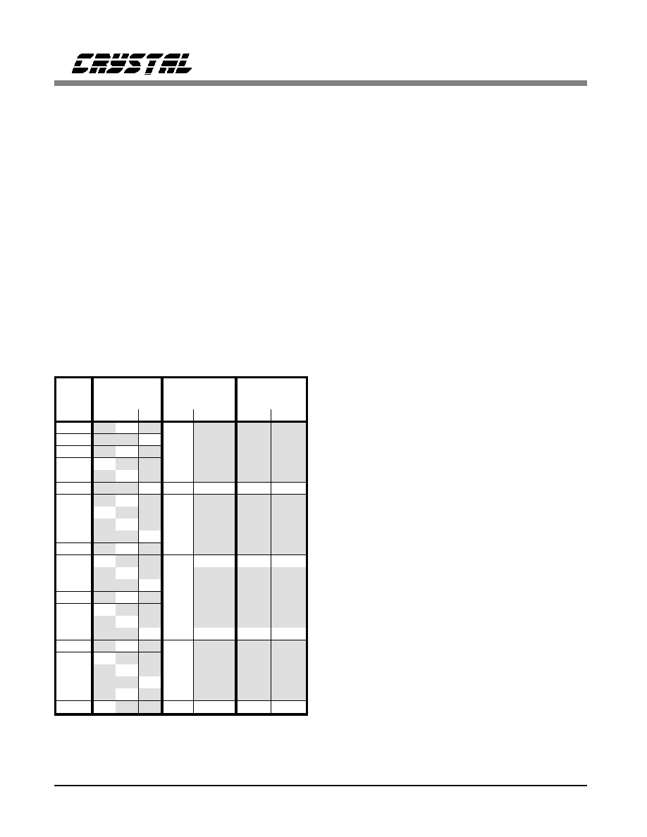
during the 6
th
and 12
th
frames. The original LSB
of the channel is actually replaced with the sig-
naling data, hence this is known as "robbed-bit"
signaling. The 6
th
and 12
th
frames can be treated
as one, 2-state channel, allowing a 2-state signal
to be updated twice every superframe. The two
frames can also be treated as separate channels
(A and B), yielding up to 4 separate codes for
each channel every superframe. For voice grade
applications, these signaling bits offer no notice-
able degradation in the signal quality. When
error-free data transmission is required however,
robbed bit signaling can be disabled (transparent
mode), and some other signaling facility must be
provided by the host system.
193E Framing Format
The 193E or Extended Superframe Format al-
lows much greater flexibility in both the use of
the framing bits, and the number of signaling
channels provided. As shown in Figure A6, the
framing bits are divided into 3 channels. The
FPS, or Framing Pattern Sequence, provides a
synchronization signal for determining frame and
superframe alignment. The FDL, or 4 kHz Facil-
ity Data Link, provides a dedicated channel for
system messages. The CRC (Cyclic Redundancy
Check) channel allows CRC check sums to be
transmitted with each superframe to monitor line
quality. As with the 193S format, every 6th
frame is designated as a signaling frame. The 4
signaling frames (6, 12, 18, and 24) can be mul-
tiplexed in different configurations to provide 2,
4, or 16-state signaling codes.
SLC-96
Æ
Framing Format
The SLC-96
Æ
T1 format is used between the Lo-
cal Digital Switch (LDS) and a SLC-96
Æ
Remote Terminal (RT). The framing format is a
SF(D4
Æ
) superframe format with specialized
Data Link (DL) information bits. The DL bits
consist of Concentrator (C), Spoiler (S), Mainte-
nance (M), Alarm (A) and Protection Line
Switch (PLS) bits as shown in Figure A7.
T1DM Framing Format
The T1DM T1 format is used for DDS
Æ
service
among hub and local intermediate DDS
Æ
offices.
As shown in Figure A8, the framing format is a
SF(D4
Æ
) superframe format with a specialized
channel 24 structure. The T1DM accepts up to
23 DS-0 signals and inserts one seven-bit byte
from each signal into the first twenty-three 8-bit
channel slots of the DS1 frame. The 24th chan-
nel slot contains a special synchronizing byte as
shown in Figure A9. DDS
Æ
equipment insures
that every DS0 channel contains at least one "1".
Therefore, neither B8ZS nor bit-7 zero substitu-
tion should be selcted in the CS62180B.
193E
F-bits
Channel
bits
Signaling
Options
Frame
FPS FDL CRC
Data
Signaling
T
2
4
16
1
m
1-8
2
C1
3
m
4
0
5
m
6
C2
1-7
Bit 8
-
A
A
A
7
m
1-8
8
0
9
m
10
C3
11
m
12
1
1-7
Bit 8
-
A
B
B
13
m
1-8
14
C4
15
m
16
0
17
m
18
C5
1-7
Bit 8
-
A
A
C
19
m
1-8
20
1
21
m
22
C6
23
m
24
1
1-7
Bit 8
-
A
B
D
Figure A6. 193E Framing Format
CS62180A
CS62180B
46
DS225PP1

Bit
Assignment
0
Synchronization Pattern = 1
1
Synchronization Pattern = 0
2
Synchronization Pattern = 1
3
Synchronization Pattern = 1
4
Synchronization Pattern = 1
5
Yellow Alarm: 0 = alarm; 1 = no alarm
6
8 kHz Data Link ("A" channel)
7
Synchronization Pattern = 0
Figure A9. T1DM Channel 24 Format
SLC-96
Æ
F-bits
Channel bits
SLC-96
Æ
F-bits
Channel bits
Frame
F
T
F
S
DL
Data
Signaling
Frame
F
T
F
S
DL
Data
Signaling
1
1
1-8
37
1
1-8
2
0
38
S=0
3
0
39
0
4
0
40
M1
5
1
41
1
6
1
1-7
Bit 8 (A)
42
M2
1-7
Bit 8 (A)
7
0
1-8
43
0
1-8
8
1
44
M3
9
1
45
1
10
1
46
A1
11
0
47
0
12
C1
1-7
Bit 8 (B)
48
A2
1-7
Bit 8 (B)
13
1
1-8
49
1
1-8
14
C2
50
PLS1
15
0
51
0
16
C3
52
PLS2
17
1
53
1
18
C4
1-7
Bit 8 (A)
54
PLS3
1-7
Bit 8 (A)
19
0
1-8
55
0
1-8
20
C5
56
PLS4
21
1
57
1
22
C6
58
S=1
23
0
59
0
24
C7
1-7
Bit 8 (B)
60
0
1-7
Bit 8 (B)
25
1
1-8
61
1
1-8
26
C8
62
0
27
0
63
0
28
C9
64
0
29
1
65
1
30
C10
1-7
Bit 8 (A)
66
1
1-7
Bit 8 (A)
31
0
1-8
67
0
1-8
32
C11
68
1
33
1
69
1
34
S=0
70
1
35
0
71
0
36
S=1
1-7
Bit 8 (B)
72
0
1-7
Bit 8 (B)
Figure A7. SLC-96
Æ
Framing Format
T1DM
F-bits
Channel
Bits
Frame
F
T
F
S
1
1
1-7
(Bit 8 of user channels is
reserved for network use)
2
0
3
0
4
0
5
1
6
1
7
0
8
1
9
1
10
1
11
0
12
0
Figure A8. T1DM Framing Format
CS62180A
CS62180B
DS225PP1
47

Alarms
Figure A10 shows a useful overview of the alarm
operation in a PCM link. When an intermediate
monitoring system (or central office repeater) de-
tects a loss of signal, it transmits an all "1's"
signal (Blue alarm, or Alarm Indication Signal)
on the line to maintain clock recovery operation
in the subsequent digital repeaters and the desti-
nation's receiver. The same Blue alarm may be
used by the source transmitter if, for some rea-
son, it cannot maintain normal functionality
(such as during loopback).
When the loss of signal is detected at the inter-
mediate monitor, an internal Red alarm (also
known as a Service Alarm Indication, or Prompt
Maintenance Alarm) is generated. While in a
Red alarm mode, the monitor transmits a Yellow
alarm back to the source's receiver, indicating a
remote loss of alignment. This Yellow alarm in-
forms the source that there's a problem farther
down the line and it's transmission is not being
received at the destination.
Zero Substitution
As was mentioned in the T1 overview, data is
transmitted over dual twisted-pair cable with
digital repeaters at 6000 ft. intervals. It is en-
coded in a bipolar AMI (Alternate Mark
Inversion) format. Successive "1's" are encoded
alternately as positive and negative voltage
pulses. A zero is simply an absence of pulses.
This means that a long stream of "0's" is indis-
tinguishable from a dead line. Clock recovery
circuits in the network maintain clock synchroni-
zation by syncing to the "1's" pulses in the
transmission stream. Synchronization may be
lost if there are too many consecutive zero's,
hence there is a general requirement that there be
at least 12.5 % "1's" density in the transmission
stream. Furthermore, no more than 15 consecu-
tive "0's" are allowable. Various zero substitution
schemes have been developed to meet these re-
quirements. The CS62180A and CS62180B
supports B7 and B8ZS zero suppression formats.
B7 Zero Substitution
B7 zero substitution guarantees at least one "1"
in all DS0 channels. This satasfies the 12.5 %
ones density, and guarantees that more than 15
consecutive zeros will never occur. In B7 substi-
tution systems, the 7
th
bit (2
nd
LSB) of an all
zero channel is forced to a "1". This strategy
maintains 1's density in voice grade transmis-
sion, with negligible audible interference. The
drawback with the B7 format is that it's impossi-
ble for the receiving end to detect and remove
the changed bits. This makes B7 zero suppres-
sion unacceptable for clear channel transmission,
in which the integrity of the data must be main-
tained.
B8ZS Zero Substitution
B8ZS (Bipolar Eight Zero Substitution) satisfies
the one's density requirement without corrupting
transmission data. Instead of operating on indi-
vidual channels, the B8ZS format looks at the
entire transmission stream. Any eight consecutive
zeros are replaced with an 8 bit code. This code
uses specific bipolar violations of the AMI for-
mat to distinguish it from the ordinary data. If
the last "1" transmitted before a string of zeros
was encoded as a positive pulse, then the B8ZS
code for the next eight bits will be 000+-0-+.
Similarly, if the last "1" was a negative pulse,
then the code will be 000-+0+-. In either case,
bipolar violations occur in the fourth and seventh
bits. These violations are decoded as a string of
Blue Alarm
Monitor
Loss of
Signal = Red
Alarm
Yellow Alarm
Source
Transmit
Receive
Transmit
Receive
Destination
Digital
Repeater
Yellow
Alarm
Yellow
Alarm
Blue
Alarm
Figure A10. Alarm Operation on a T1 Link.
CS62180A
CS62180B
48
DS225PP1

zeros by the CS62180A and CS62180B if B8ZS
is enabled. The received B8ZS code is replaced
with eight zeros before any other processing is
done on the incoming data. Note also that even
if B8ZS is not enabled, the CS62180A and
CS62180B monitors the incoming signal for
B8ZS codes, and reports them on RSR.2 (if
CCR.6 = 0).
A serious provisioning problem exists in the net-
work regarding B8ZS. It is sometimes difficult to
selectively turn-on B8ZS on all segments of an
end-to-end path through the network, especially
when some equipment types, such as M13s,
sometimes require that all four lines on a line
card be configured the same way. It is thereby
highly desireable that all receivers in the network
be able to receive B8ZS independent of the pro-
visioning of B8ZS on the corresponding
transmitter. Therefore, the CS62180B has its
B8ZS receiver turned on all of the time, and bit
CCR.2 controls only the B8ZS encoder in the
transmitter. The CS62180B reports B8ZS occur-
rences on RSR.2. B8ZS substitutions will not
increment the Bipolar Violation Count register.
Digital Milliwatt Code
The Digital Milliwatt code is the digital repre-
sentation of a 0 dBm0, 1 kHz signal. It's used as
a test reference for calibrating channel bank
equipment as specified in AT&T Publication
43801.
Schematic & Layout Review Service
Confirm Optimum
Schematic & Layout
Before Building Your Board.
For Our Free Review Service
Call Applications Engineering.
C a l l : ( 5 1 2 ) 4 4 5 - 7 2 2 2
The Crystal logo and SMARTAnalog
TM
are trademarks of Crystal Semiconductor.
D4
Æ
, DDS
Æ
, and SLC-96
Æ
are registered trademarks of AT&T.
CS62180A
CS62180B
DS225PP1
49

∑ Notes ∑

∑ Notes ∑

Smart
Analog
TM
is a Trademark of Crystal Semiconductor Corporation