 | –≠–ª–µ–∫—Ç—Ä–æ–Ω–Ω—ã–π –∫–æ–º–ø–æ–Ω–µ–Ω—Ç: CS7410 | –°–∫–∞—á–∞—Ç—å:  PDF PDF  ZIP ZIP |
Preliminary Product Information
This document contains information for a new product.
Cirrus Logic reserves the right to modify this product without notice.
1
Copyright
©
Cirrus Logic, Inc. 2002
(All Rights Reserved)
Cirrus Logic, Inc.
P.O. Box 17847, Austin, Texas 78760
(512) 445 7222 FAX: (512) 445 7581
http://www.cirrus.com
CS7410
CD/MP3/WMA Audio Controller
Features
l
Super on-chip Integration for low cost and low count bill of
materials
l
32-Bit RISC Processor performs audio decode and system
management functions
l
16-bit DSP for audio special effects
l
80 Kbytes internal SRAM, and 256 Kbytes internal ROM
l
Interfaces to external SDRAM or EDO DRAM (for shock
protection), and to external ROM/FLASH (for custom
program storage)
l
CD serial interface with advanced pattern matching and
software error handling
l
Integrated DAC functionality
l
Simultaneous 4 channels PCM audio output and IEC-958
output.
l
Large number of GPIO pins for servo control, key scan, LCD
control, etc.
l
Three serial control/status ports
l
Sophisticated clock management and low power
consumption
l
Supports ISO9660 and multi-session write methods
l
Low power 0.18 micron technology
l
100-pin MQFP package
l
100-pin LQFP package
Description
The CS7410 is a true system-on-a-chip for the CD-
based digital audio market. With a powerful RISC pro-
cessor, one DSP, integrated audio
modulator, large
internal SRAM and program ROM, and glueless inter-
face to popular CD chip sets, the CS7410 is a complete
single chip low-power programmable audio decoder.
This powerful architecture is easily capable of MP3,
WMA, and other future audio formats. The CS7410's
flexible architecture and low power consumption make it
an ideal low-cost solution for a wide range of player ap-
plications. For portable audio systems, the memory
interface can be used to add DRAM or SRAM for Elec-
tronic Shock Protection (ESP). A flexible set of interfaces
are available for end-user I/O such as a keypad and LCD
control for use in mass market CD players, boom boxes,
and shelf-top systems.
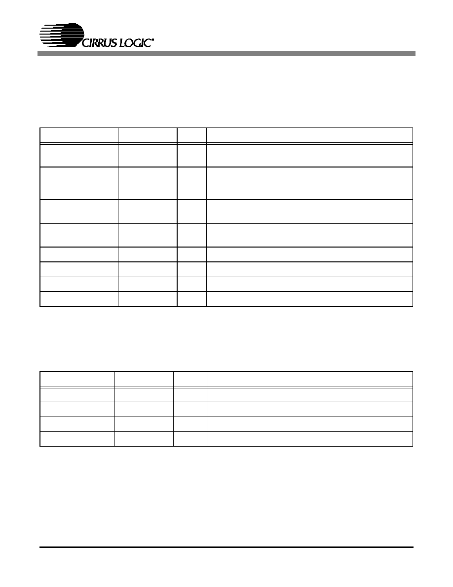
ORDERING INFORMATION
CS7410-CM
0∞ to 70∞ C
100-pin MQFP
CS7410-CQ
0∞ to 70∞ C
100-pin LQFP
Audio
Interface
Modulator
PCM Out
IEC-958
X,Y Data
memory
CPU / MAC
Instruction
Cache
80 KB
Internal
SRAM
256 KB
Internal
ROM
DRAM
Control
Mini
DMA
ROM/SRAM
Control
Flash
Control
Memory Controller
Register
Bank
System Miscellaneous
Clock
Control
Timers
Get Bits
Data
Cache
Instruction
Cache
CPU
MAC
CD
Interface
PLL
Control
FIFO
External Interface
2-Wire Debug Interface
3/4 Wire Serial
Programmable I/O
PWM Out
RISC-32
DSP-16
JUL `02
DS553PP1

CS7410
2
DS553PP1
TABLE OF CONTENTS
1. CHARACTERISTICS AND SPECIFICATIONS ........................................................................ 5
1.1 AC and DC Parametric Specifications ............................................................................... 5
1.1.1 Absolute Maximum Rating .................................................................................... 5
1.1.2 Recommended Operating Conditions ................................................................... 5
1.1.3 Electrical Specifications ........................................................................................ 5
1.1.4 DC Characteristics ................................................................................................ 7
1.1.4.1 SDRAM Interface .................................................................................. 7
1.1.4.2 Serial Interface .................................................................................... 11
1.1.4.3 EDO DRAM interface .......................................................................... 12
1.1.4.4 FLASH / ROM Interface ...................................................................... 15
1.1.4.5 Audio Output Interface ........................................................................ 17
1.1.4.6 CD Interface ........................................................................................ 18
1.1.4.7 Miscellaneous Timings ........................................................................ 20
2. CS7410 SUMMARY ................................................................................................................ 21
2.1 CS7410 Typical Application ............................................................................................. 21
2.2 CS7410 Block Summaries .............................................................................................. 21
2.2.1 RISC-32 .............................................................................................................. 21
2.2.2 DSP-16 ................................................................................................................ 21
2.2.3 System Controls .................................................................................................. 21
2.2.4 Memory System .................................................................................................. 22
2.2.5 CD Interface ........................................................................................................ 22
2.2.6 Audio Interface .................................................................................................... 22
2.2.7 External Interface ................................................................................................ 22
2.2.8 System Functions ................................................................................................ 22
3. FUNCTIONAL DESCRIPTION ............................................................................................... 23
3.1 RISC-32 Processor .......................................................................................................... 23
3.2 DSP-16 Processor ........................................................................................................... 23
3.3 Memory Control ............................................................................................................... 23
3.4 CD Interface ..................................................................................................................... 23
3.5 System Control Functions ................................................................................................ 23
3.6 Audio Output .................................................................................................................... 24
4. PIN DESCRIPTION ................................................................................................................. 25
Contacting Cirrus Logic Support
For a complete listing of Direct Sales, Distributor, and Sales Representative contacts, visit the Cirrus Logic web site at:
http://www.cirrus.com/corporate/contacts/sales.cfm
IMPORTANT NOTICE
"Preliminary" product information describes products that are in production, but for which full characterization data is not yet available. "Advance" product infor-
mation describes products that are in development and subject to development changes. Cirrus Logic, Inc. and its subsidiaries ("Cirrus") believe that the infor-
mation contained in this document is accurate and reliable. However, the information is subject to change without notice and is provided "AS IS" without warranty
of any kind (express or implied). Customers are advised to obtain the latest version of relevant information to verify, before placing orders, that information being
relied on is current and complete. All products are sold subject to the terms and conditions of sale supplied at the time of order acknowledgment, including those
pertaining to warranty, patent infringement, and limitation of liability. No responsibility is assumed by Cirrus for the use of this information, including use of this
information as the basis for manufacture or sale of any items, or for infringement of patents or other rights of third parties. This document is the property of Cirrus
and by furnishing this information, Cirrus grants no license, express or implied under any patents, mask work rights, copyrights, trademarks, trade secrets or
other intellectual property rights. Cirrus owns the copyrights of the information contained herein and gives consent for copies to be made of the information only
for use within your organization with respect to Cirrus integrated circuits or other parts of Cirrus. This consent does not extend to other copying such as copying
for general distribution, advertising or promotional purposes, or for creating any work for resale.
An export permit needs to be obtained from the competent authorities of the Japanese Government if any of the products or technologies described in this ma-
terial and controlled under the "Foreign Exchange and Foreign Trade Law" is to be exported or taken out of Japan. An export license and/or quota needs to be
obtained from the competent authorities of the Chinese Government if any of the products or technologies described in this material is subject to the PRC Foreign
Trade Law and is to be exported or taken out of the PRC.
CERTAIN APPLICATIONS USING SEMICONDUCTOR PRODUCTS MAY INVOLVE POTENTIAL RISKS OF DEATH, PERSONAL INJURY, OR SEVERE
PROPERTY OR ENVIRONMENTAL DAMAGE ("CRITICAL APPLICATIONS"). CIRRUS PRODUCTS ARE NOT DESIGNED, AUTHORIZED, OR WARRANT-
ED TO BE SUITABLE FOR USE IN LIFE-SUPPORT DEVICES OR SYSTEMS OR OTHER CRITICAL APPLICATIONS. INCLUSION OF CIRRUS PRODUCTS
IN SUCH APPLICATIONS IS UNDERSTOOD TO BE FULLY AT THE CUSTOMER'S RISK.
Cirrus Logic, Cirrus, and the Cirrus Logic logo designs are trademarks of Cirrus Logic, Inc. All other brand and product names in this document may be trade-
marks or service marks of their respective owners.

CS7410
DS553PP1
3
4.1 Pin Identification .............................................................................................................. 25
4.2 Miscellaneous Pins .......................................................................................................... 30
4.3 Serial Interface Pins ........................................................................................................ 30
4.4 SDRAM / DRAM Interface ............................................................................................... 31
4.5 ROM/NVRAM Interface ................................................................................................... 32
4.6 Digital Audio Output Interface .......................................................................................... 33
4.7
Modulator Interface .................................................................................................... 33
4.8 CD Interface .................................................................................................................... 34
4.9 General Purpose Input/Output (GPIO) ............................................................................ 35
4.10 Power and Ground ........................................................................................................ 36
5. 100-PIN MQFP PACKAGE SPECIFICATIONS (20X14X2.85MM) ....................................... 38
6. 100-PIN LQFP PACKAGE SPECIFICATIONS (14X14X1.4MM) ........................................... 39
LIST OF FIGURES
Figure 1. SDRAM Timing ................................................................................................................ 7
Figure 2. SDRAM Load Mode ......................................................................................................... 8
Figure 3. SDRAM Burst Write ......................................................................................................... 9
Figure 4. SDRAM Burst Read ......................................................................................................... 9
Figure 5. SDRAM Refresh ............................................................................................................ 10
Figure 6. Serial Interface Timing Diagram .................................................................................... 11
Figure 7. EDO Page Write Timing Diagram .................................................................................. 13
Figure 8. EDO Page Read Timing Diagram.................................................................................. 13
Figure 9. EDO Refresh Timing Diagram ....................................................................................... 14
Figure 10. FLASH/ROM Read ...................................................................................................... 15
Figure 11. FLASH/ROM Write....................................................................................................... 16
Figure 12. Audio Output Timing .................................................................................................... 17
Figure 13. CD Interface Timing ..................................................................................................... 18
Figure 14. CD Interface Timing Diagrams..................................................................................... 19
Figure 15. Miscellaneous Timings................................................................................................. 20
Figure 16. CS7410 Application ..................................................................................................... 21
Figure 17. CS7410 Pin Identification............................................................................................. 25
Figure 18. 100-Pin MQFP Package (20x14x2.85mm) .................................................................. 38
Figure 19. 100-Pin LQFP Package (14X14X1.4mm).................................................................... 39
LIST OF TABLES
Table 1. SDRAM Characterization Data ......................................................................................... 7
Table 2. Serial Interface Characterization Data ............................................................................ 11
Table 3. EDO DRAM Characterization Data ................................................................................. 12
Table 4. FLASH/ROM Read Characterization Data...................................................................... 15
Table 5. Audio Output Interface Symbols and Characterization Data........................................... 17
Table 6. Pin Type and Direction Legend....................................................................................... 25
Table 7. Pin Assignments ............................................................................................................. 26
Table 8. Miscellaneous Interface Pins .......................................................................................... 30
Table 9. Serial Interface Pins........................................................................................................ 30
Table 10. SDRAM Interface .......................................................................................................... 31
Table 11. EDO DRAM Interface.................................................................................................... 31
Table 12. ROM/NVRAM Interface................................................................................................. 32
Table 13. Audio Output Interface .................................................................................................. 33
Table 14.
Output Interface....................................................................................................... 33
Table 15. CD Interface .................................................................................................................. 34

CS7410
4
DS553PP1
Table 16. Dedicated General Purpose I/O Pins ............................................................................ 35
Table 17. Redefined General Purpose Pins.................................................................................. 35
Table 18. Power and Ground ........................................................................................................ 36

CS7410
DS553PP1
5
1. CHARACTERISTICS AND SPECIFICATIONS
1.1
AC AND DC PARAMETRIC SPECIFICATIONS
(AGND, DGND=0V, all voltages with respect to 0V)
1.1.1
Absolute Maximum Rating
CAUTION: Operating beyond these Minimum and Maximum limits can result in permanent damage to
the device. Cirrus Logic recommends that CS7410 devices operate at the settings described in the next ta-
ble.
1.1.2
RECOMMENDED OPERATING CONDITIONS
1.1.3
Electrical Specifications
(TA = 0 to 70
o
C)
Symbol
Description
Min.
Max.
Unit
VDD
IO
Power Supply Voltage on I/O ring
-0.5
4.6
Volts
VDD
CORE
Power Supply Voltage on core logic and PLL
-0.5
2.5
Volts
V
I
Digital Input Applied Voltage (power applied)
-0.5
5.5
Volts
I
I
Digital Input Forced Current
-10
10
mA
I
O
Digital Output Forced Current
-50
50
mA
T
SOL
Lead Soldering Temperature
260
o
C
T
VSOL
Vapor Phase Soldering Temperature
235
o
C
T
STOR
Storage Temperature (no power applied)
-40
125
o
C
T
AMB
Ambient Temperature (power applied)
0
70
o
C
P
TOT
Power consumption
1
W
Parameter
Symbol
Min
Typ
Max
Units
Supply Voltage, IO
V
DD
3.0
3.3
3.6
Volts
Supply Voltage, core and PLL
V
DD
1.62
1.8V
1.98
Volts
Ambient Temperature (power applied)
T
AMB
0
25
70
o
C
Parameter
Symbol
Conditions
Min
Typ
Max
Units
Power Supply
Supply Current, IO
I
DD
Normal Operating
13
mA
Supply Current, core and PLL
I
DD
Normal Operating
70
mA
CS7410
6
DS553PP1
Digital Pins
Input Voltage, High
V
IH
2.0
Volts
Input Voltage, Low
V
IL
0.8
Volts
Input Current
I
IN
V
IN
= V
DD
or V
SS
-1
+1
µ
A
Input Pull up/down resistor
R
I
75
K
Output Voltage, High
V
OH
@ buffer rating
2.4
Volts
Output Voltage, Low
V
OL
@ buffer rating
0.4
Volts
High-Z-state Leakage
I
OZ
V
OUT
= V
SS
or V
DD
-1
+1
µ
A
Parameter
Symbol
Conditions
Min
Typ
Max
Units
CS7410
DS553PP1
7
1.1.4
DC CHARACTERISTICS
(TA= 25∞C; VDD_PLL=VDD_CORE=1.8V±10%, VDD_IO=3.3V±10%)
1.1.4.1
SDRAM Interface
Symbol
Description
Min
Typ
Max
Unit
t
mper
DR_CKO Period
22
ns
t
mco
Output Delay from DR_CKO active edge
19
ns
t
mdow
M_D[15:0] delay from DR_CKO
19
ns
t
mhw
M_D[15:0] valid time after DR_CKO
5
ns
t
msur
M_D[15:0] setup to DR_CKO
13
ns
t
mhr
M_D[15:0] hold time after DR_CKO
0
ns
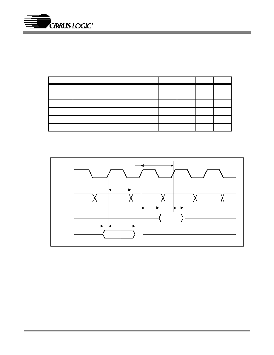
Table 1. SDRAM Characterization Data
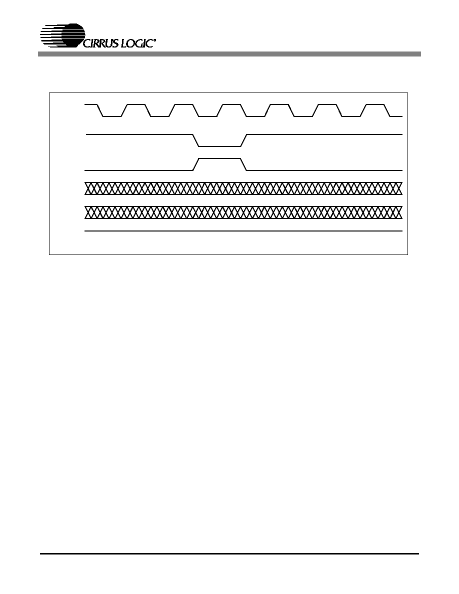
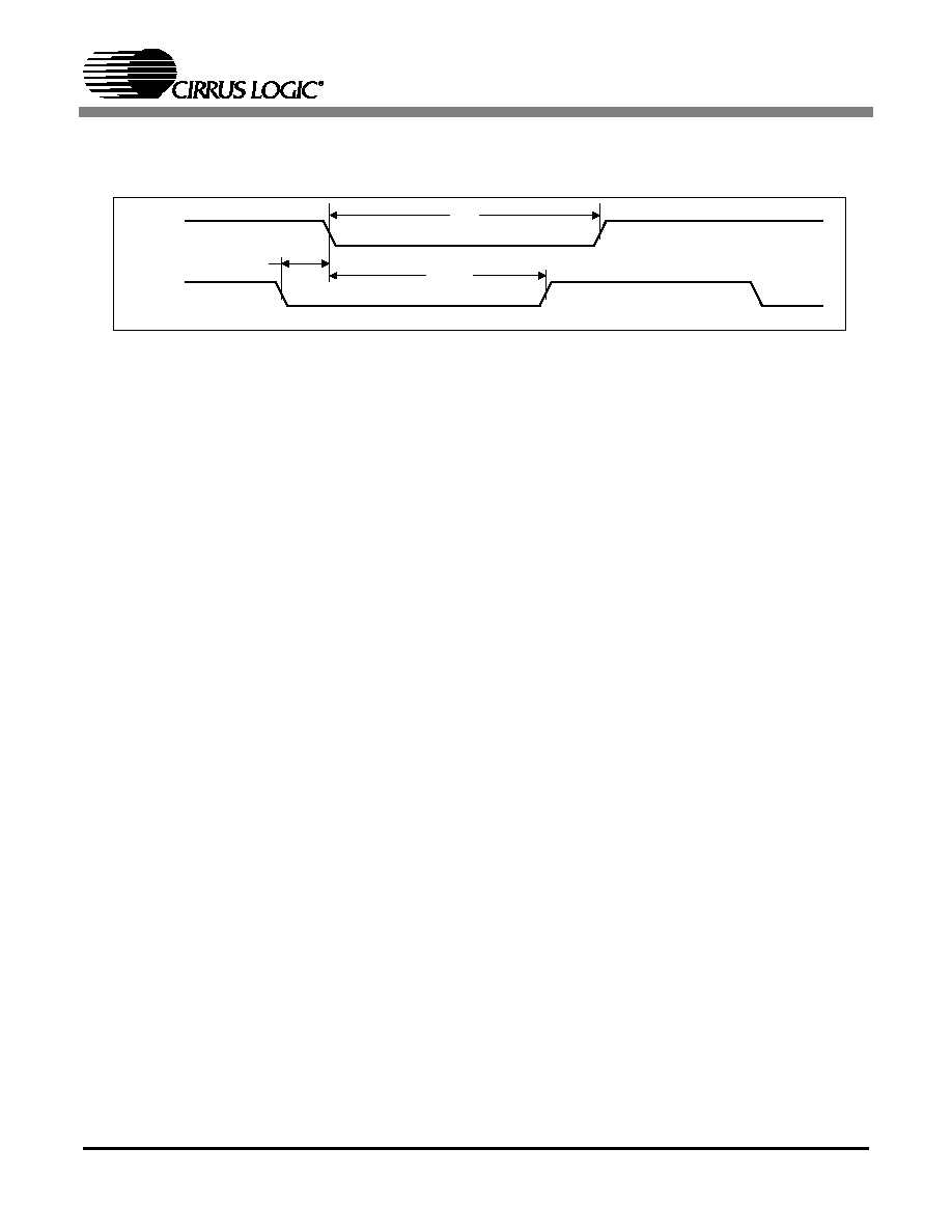
DR_CKO
DR_RAS_L
DR_CAS_L
M_A
M_D
(write)
M_WE_L
t
mper
t
mdow
M_D
(read)
t
msur
t
mhr
t
mhw
t
mco
Figure 1. SDRAM Timing
CS7410
8
DS553PP1
DR_CKO
DR_RAS_L
DR_CAS_L
M_A
M_D
M_WE_L
Figure 2. SDRAM Load Mode

CS7410
DS553PP1
9
DR_CKO
DR_RAS_L
DR_CAS_L
M_A
M_D
M_WE_L
D0
ADRAS
ADCAS
Dn
...
D1
Figure 3. SDRAM Burst Write
ADRAS
ADCAS
DR_CKO
DR_RAS_L
DR_CAS_L
M_A
M_D
M_WE_L
D1
Dn
...
D2
Figure 4. SDRAM Burst Read
CS7410
10
DS553PP1
DR_CKO
DR_RAS_L
DR_CAS_L
M_WE_L
M_A
M_D
Figure 5. SDRAM Refresh
CS7410
DS553PP1
11
1.1.4.2
Serial Interface
Symbol
Description
Min
Typ
Max
Unit
t
clk_per
Clock period
66
ns
t
DMs
Master-mode data setup
28
ns
t
DMh
Master-mode data hold
28
ns
t
DSs
Slave-mode data setup
15
ns
t
CMs
Master chip select to clock setup
28
ns
t
DSh
Slave mode data hold
0
ns
Table 2. Serial Interface Characterization Data
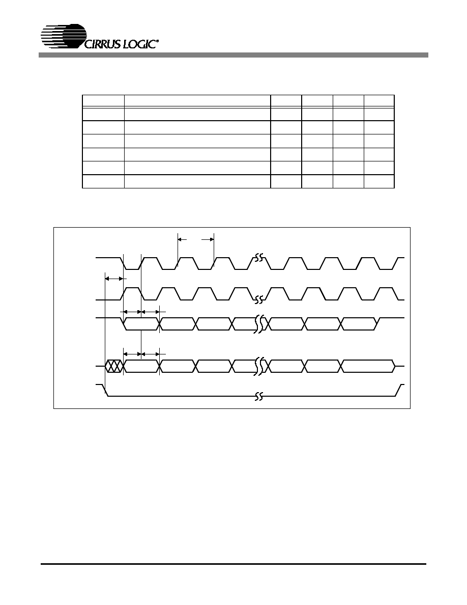
SER2_CLK
(CPOL=0)
SER2_CLK
(CPOL=1)
SER2_DO
(master)
SER2_DI
(slave)
SER2_CS
MSB
LSB
LSB
MSB
t
clk_per
t
DMs
t
DMh
t
DSs
t
DSh
t
CMs
Figure 6. Serial Interface Timing Diagram
CS7410
12
DS553PP1
1.1.4.3
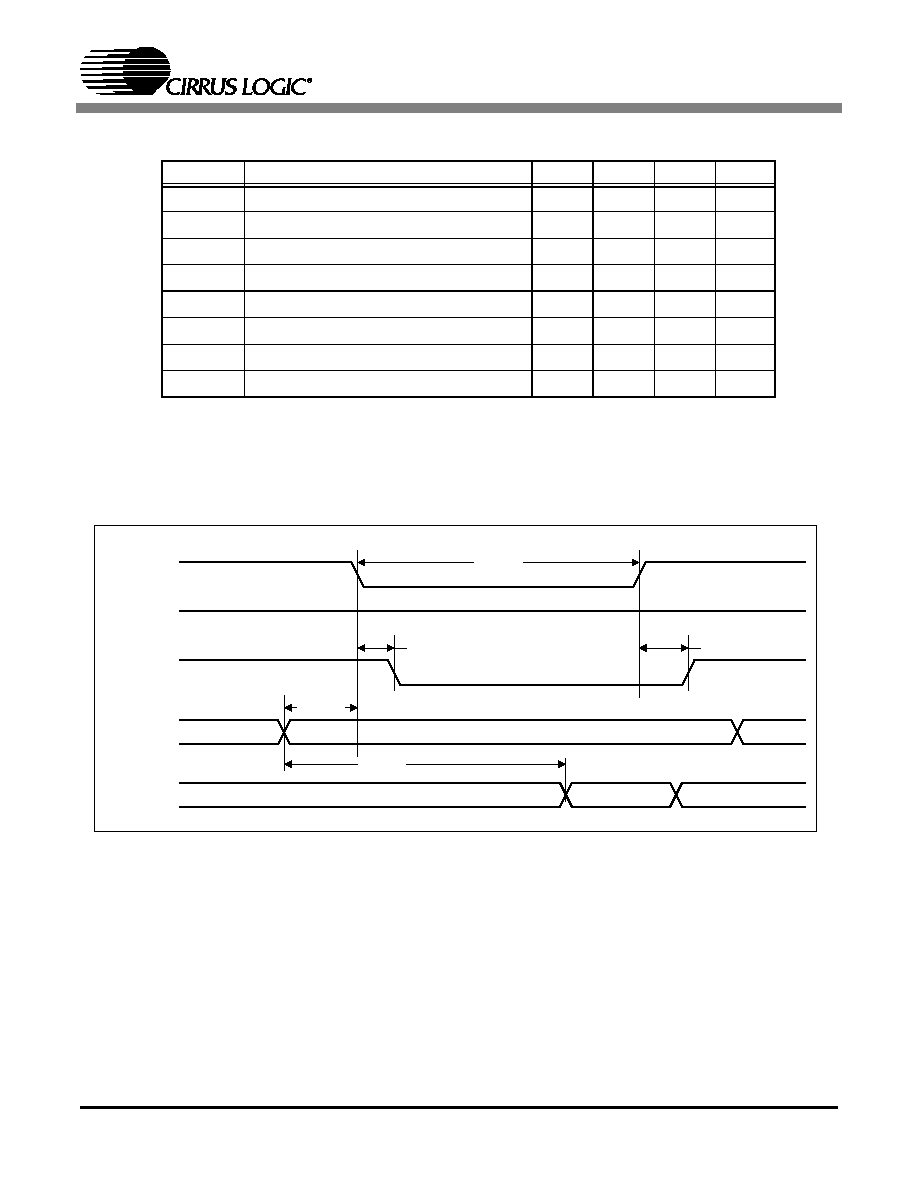
EDO DRAM interface
Note:Values shown are for minimum internal clock period (11ns) and all programmed wait states enabled.
Symbol
Description
Min
Typ
Max
Unit
t
RAS
RAS low time
72
ns
t
RP
RAS high pulse time
40
ns
t
RCL
RAS fall to CAS fall
38
ns
t
CAS
CAS low time
30
ns
t
CPN
CAS high time
15
ns
t
CAH
CAS fall to address row
29
ns
t
ASR
Address row to RAS fall
10
ns
t
RAH
RAS fall to address column
18
ns
t
ASC
second address column (burst) to CAS fall 10
ns
t
AA
Column address to data setup
35
ns
t
CAC
CAS fall to data setup
17
ns
t
CSR
CAS fall to RAS fall
19
ns
t
CHR
RAS fall to CAS rise
18
ns
t
CRH
CAS rise to RAS rise
6
ns
t
WDS
Write data setup to CAS fall
12
ns
t
WDH
Write data hold to CAS fall
29
ns
t
WS
Write enable setup to CAS fall
13
ns
t
WH
Write enable hold to CAS fall
20
ns
t
ROE
RAS fall to OE fall
-5
5
ns
t
OER
RAS rise to OE rise
-5
5
ns
t
DCH
Read data hold to CAS rise
0
ns
Table 3. EDO DRAM Characterization Data
CS7410
DS553PP1
13
ADRAS
ADCAS
DR_RAS_L
DR_CAS_L
M_A
M_D
M_AP_WE
DATA
DATA
t
ASR
t
RAH
t
RCL
t
CPN
ADCAS
t
ASC
t
CAH
t
CAS
t
RAS
t
RP
t
CRH
t
WS
t
WH
t
WDS
t
WDH
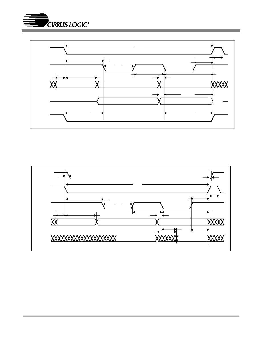
Figure 7. EDO Page Write Timing Diagram
ADRAS
ADCAS
DR_RAS_L
DR_CAS_L
M_A
M_D
M_AP_OE
DATA
DATA
t
ASR
t
RAH
t
RCL
t
CPN
ADCAS
t
ASC
t
CAH
t
AA
t
CAC
t
CAS
t
RAS
t
RP
t
ROE
t
CRH
t
DCH
t
OER
Figure 8. EDO Page Read Timing Diagram
CS7410
14
DS553PP1
DR_RAS_L
DR_CAS_L
t
CSR
t
CHR
t
RAS
Figure 9. EDO Refresh Timing Diagram
CS7410
DS553PP1
15
1.1.4.4
FLASH / ROM Interface
Note:Values shown are for minimum internal clock period (11ns) and no programmed wait states.
Symbol
Description
Min
Typ
Max
Unit
t
CSpw
CE low period
135
ns
t
RDd1
CE fall to output enable fall
5
ns
t
RDd2
CE rise to output enable rise
-5
5
ns
t
ADs
Address setup to CE fall
-10
10
ns
t
DAs
Data setup after address
1
28
ns
t
WRSU
All outputs setup before WE
95
ns
t
WRPW
WE pulse width
170
ns
t
WRH
All outputs hold after WE
95
ns
Table 4. FLASH/ROM Read Characterization Data
1.
Value shown for 3 programmed wait states.
NVM_CE_L
M_WE_L
M_AP_OE
M_A
M_D
t
ADs
t
CSpw
t
RDd1
t
RDd2
t
DAS
Figure 10. FLASH/ROM Read
CS7410
16
DS553PP1
NVM_CE_L
M_AP_OE
M_A
M_D
M_WE_L
t
WRSU
t
WRH
t
WRPW
Figure 11. FLASH/ROM Write
CS7410
DS553PP1
17
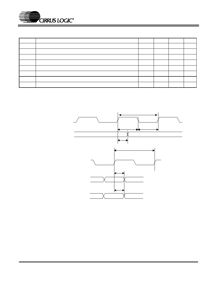
1.1.4.5
Audio Output Interface
Symbol
Description
Min
Typ
Max
Units
t
axch
PCM_XCLK High Time (PCM_XCLK is Input/Output)
42
50
%
t
axcl
PCM_XCLK Low Time (PCM_XCLK is Input/Output
42
50
%
t
axper
PCM_XCLK period (Input/Output)
55
ns
t
aoper
PCM_BCK period (Output)
440
ns
t
sdmo
PCM_BCK delay from PCM_XCLK output transition
1
5
ns
t
sdmi
PCM_BCK delay from PCM_XCLK input transition
1
15
ns
t
lrds
PCM_LRCK delay from PCM_BCK transition
1
5
ns
t
adsm
PCM_D[3:0] delay from PCM_BCK transition
1
5
ns
Table 5. Audio Output Interface Symbols and Characterization Data
1.
Active clock edge is programmable. Timing is referenced from the active edge.
PCM_BCK(Output)
PCM_XCK(Input/Output)
t
sdmi
sdmo
t
axch
PCM_BCK(Output)
PCM_DO[1:0] (Output)
PCM_LRCK(Output)
t
lrds
t
adsm
t
axcl
t
axper
t
aoper
Figure 12. Audio Output Timing

CS7410
18
DS553PP1
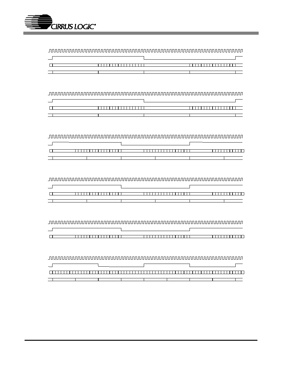
1.1.4.6
CD Interface
Note:Active edge of CD_BCLK is programmable
Symbol
Description
Min
Typ
Max
Units
t
slri
CD_LRCK setup to CD_BCK active edge
7
ns
t
sdi
CD_DATA and CD_C2P0 setup to CD_BCK active edge
7
ns
t
hsdi
CD_DATA and CD_C2P0 hold time after CD_BCK active edge
3
ns
CD_BCK(Input)*
CD_DO (Input)
CD_LRCK(Input)
CD_C2PO (Input)
t
slri
t
sdi
t
hsdi
Figure 13. CD Interface Timing
CS7410
DS553PP1
19
15
0
1
CD_BCK
CD_LRCK
DATA
C2P0
14 13 12 11 10 9 8 7 6 5 4 3 2
Invalid
0
15
0
1
14 13 12 11 10 9 8 7 6 5 4 3 2
Invalid
MSB
LSB
MSB
LSB
Lower (Left Channel)
Upper (Left Channel)
Lower (Right Channel)
Upper (Right Channel)
32-bit BCK, MSB First, Right Channel Low, C2P0 LSB First, Data latch timing high
15
0
1
CD_BCK
CD_LRCK
DATA
C2P0
14 13 12 11 10 9 8 7 6 5 4 3 2
Invalid
0
15
0
1
14 13 12 11 10 9 8 7 6 5 4 3 2
Invalid
MSB
LSB
MSB
LSB
Upper (Right Channel)
Lower (Right Channel)
Upper (Left Channel)
Lower (Left Channel)
32-bit BCK, MSB First, Left Channel Low, C2P0 MSB First, Data latch timing low
15
0
1
CD_BCK
CD_LRCK
DATA
C2P0
14 13 12 11 10 9 8 7 6 5 4 3 2
Invalid
0
MSB
LSB
Lower (Left Channel)
Upper (Left Channel)
Lower (Right Channel)
Upper (Right Channel)
24-bit BCK, MSB First, Right Channel Low, C2P0 MSB First, Data latch timing high
Left Channel
Right Channel
Right Channel
Left Channel
Left Channel
Right Channel
15
0
1
14 13 12 11 10 9 8 7 6 5 4 3 2
Invalid
MSB
LSB
15 14 13 12 11 10 9 8 7 6 5
Invalid
MSB
Upper (Left Channel)
Left Channel
CD_BCK
CD_LRCK
DATA
C2P0
Invalid
0
LSB
MSB
Lower (Left Channel)
Upper (Left Channel)
Lower (Right Channel)
Upper (Right Channel)
24-bit BCK, LSB First, Right Channel Low, C2P0 MSB First, Data latch timing low
Left Channel
Right Channel
Invalid
LSB
MSB
Invalid
LSB
Upper (Left Channel)
Left Channel
0
15
1
14
13
12
11
10
9
8
7
6
5
4
3
2
0
15
1
14
13
12
11
10
9
8
7
6
5
4
3
2
0 1
10
9
8
7
6
5
4
3
2
15
0
1
CD_BCK
CD_LRCK
DATA
14 13 12 11 10 9 8 7 6 5 4 3 2
Invalid
0
MSB
LSB
24-bit BCK, MSB First, Right Channel Low, Data latch timing high (Note: no C2P0 for this format)
Left Channel
Right Channel
15
0
1
14 13 12 11 10 9 8 7 6 5 4 3 2
Invalid
MSB
LSB
15 14 13 12 11 10 9 8 7 6 5
Invalid
MSB
Left Channel
15
0
1
CD_BCK
CD_LRCK
DATA
C2P0
14 13 12 11 10 9 8 7 6 5 4 3 2
0
MSB
LSB
Lower (Left Channel)
Upper (Left Channel)
Lower (Right Channel)
Upper (Right Channel)
16-bit BCK, MSB First, Left Channel Low, C2P0 LSB First, Data latch timing high
Left Channel
Right Channel
15
0
1
14 13 12 11 10 9 8 7 6 5 4 3 2
MSB
LSB
15
0
1
14 13 12 11 10 9 8 7 6 5 4 3 2
MSB
LSB
Lower (Left Channel)
Upper (Left Channel)
Lower (Right Channel)
Upper (Right Channel)
Left Channel
Right Channel
15
0
1
14 13 12 11 10 9 8 7 6 5 4 3 2
MSB
LSB
15 14 13
MSB
Figure 14. CD Interface Timing Diagrams
CS7410
20
DS553PP1
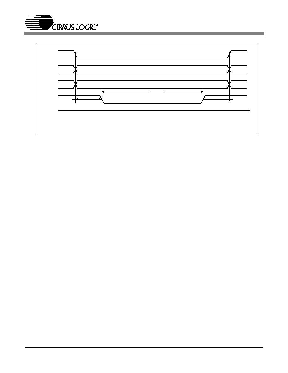
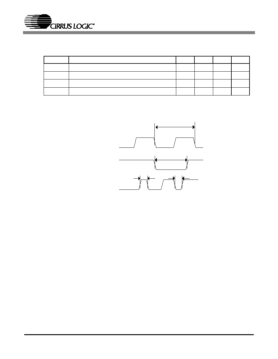
1.1.4.7
Miscellaneous Timings
Symbol
Description
Min
Typ
Max
Unit
t
xclper
1
XTLCLK period
59.05
ns
t
rstl
RST_N Low Pulse Width
1000
ns
t
gph
GPIO PW High
50
ns
t
gpl
GPIO PW Low
50
ns
1.
Value represents typical application with 16.934 MHz crystal
RESET-N
t
gph
t
gp
l
t
rst
l
XTLCLOCK
GPIO
xccper
t
Figure 15. Miscellaneous Timings

CS7410
DS553PP1
21
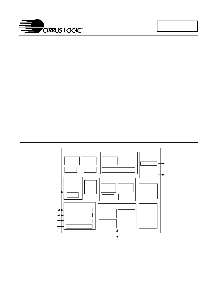
2. CS7410 SUMMARY
2.1
CS7410 Typical Application
Figure 16
shows an example of a complete audio player using the CS7410.
2.2
CS7410 Block Summaries
2.2.1
RISC-32
∑
Powerful 32-bit RISC processor
∑
Comprehensive development tool support
∑
Big or little endian data formats supported
∑
32x32 (64-bit result) MAC, 2 cycles / multiply
with C support
∑
4 Kbyte instruction cache, 2 Kbyte data cache
∑
Single cycle instructions, runs up to 90 MHz
2.2.2
DSP-16
∑
Powerful 16-bit DSP processor
∑
16-bit fixed point logic, with 36 bit accumula-
tor.
∑
Single-cycle throughput, 2-cycle latency multi-
ply accumulate, 16-bit simple integer logic
∑
512 byte instruction cache, 8 Kbyte program
visible local memory
∑
Single cycle instructions, runs up to 90 MHz
∑
DSP MAC is pipelined, 1 cycle / multiply
2.2.3
System Controls
∑
Includes 32 hardware lockable semaphore reg-
isters
∑
Two general-purpose registers for inter-proces-
Servo
DSP/Rd
Channel
Speakers/Headphones
(2 or 4 channel)
PCM
DACs
OP-AMPs
4 Chan.
Debug
Optical
Driver
2 Chan.
IEC-958
ROM/FLASH
(optional)
0-2 MB
For new code
DRAM
EDO/SDRAM
(optional)
0-8 MB
For shock protection
Serial
EEPROM
(optional)
Keypad
Matrix
LCD
Controller/
Display
IR
receiver
GPIO
Memory
Interface
Serial
Interface
Digital Audio Out
DAC
Out
CD
Interface
CS7410
Figure 16. CS7410 Application

CS7410
22
DS553PP1
sor communication
∑
Three 32-bit timers for I/O and other uses, with
programmable interval rates
∑
"Getbits" module accelerates peripheral stream
parsing
∑
Both hardware and software interrupts on data
or debug
2.2.4
Memory System
∑
Large internal SRAM (80 Kbyte) and internal
program ROM (256 Kbyte)
∑
Supports both Synchronous and EDO DRAM
(256 KBytes to 8 MBytes) for ESP
∑
Supports one bank of FLASH and ROM (up to
2 MBytes) for nonvolatile storage
∑
4-, 8-, or16-bit data bus for DRAM, 8-bit data
bus for ROM
2.2.5
CD Interface
∑
Glueless interfaces to CD servo chip set, sup-
porting all standard CD formats
∑
Includes pattern matching hardware to support
fast ESP recovery
2.2.6
Audio Interface
∑
Supports 4 channels PCM, I
2
S connectivity at
up to 24 bits
∑
Flexible audio clocking scheme using internal
PLL and dividers, or external pins
∑
Simultaneous IEC-958 output with program-
mable channel status and user data
∑
Integrated sigma-delta (
) stereo audio mod-
ulator
2.2.7
External Interface
∑
2-wire serial slave port, used for debug
∑
3- or 4-wire synchronous serial master/slave
port for external controller or slave peripheral
∑
Separate synchronous serial master port opti-
mized for receiving CD sub-codes
∑
Up to 29 programmable bi-directional I/O
(GPIO) and up to 9 output only (GPO) pins
(some multiplexed with other peripherals)
∑
All pins defined as GPIOs can be used to re-
ceive edge or level detection interrupts.
∑
Pulse-width modulated (PWM) output pin can
be used to create simple ADC using low-cost
comparator (i.e., for battery voltage monitor)
2.2.8
System Functions
∑
Internal oscillator uses external crystal, or re-
ceives clock (i.e. 16.9 MHz) from CD servo
∑
Internal PLL generates any system clock fre-
quency, chip can run up to 90 MHz
∑
Includes clock divider and clock shutoff cir-
cuits for low power/sleep modes
∑
Advanced 0.18 micron CMOS technology,
runs off 1.8 V and 3.3 V
∑
All I/O pins are 3.3 V, with 5 V tolerance
∑
100-pin MQFP package
∑
100-pin LQFP package

CS7410
DS553PP1
23
3. FUNCTIONAL DESCRIPTION
3.1
RISC-32 Processor
The CS7410 includes a powerful, proprietary 32-
bit RISC processor backed by powerful software
development tools. The RISC-32 has a MAC en-
gine which performs multiply/accumulate in 2 cy-
cles with C support, effectively achieving single
cycle throughput.
There are other instructions that are designed to
help with performing audio decoding. The RISC
processor coordinates on-chip multi-threaded
tasks, as well as supervises system activities such
as keypad and front panel display control.
3.2
DSP-16 Processor
The CS7410 contains a proprietary digital signal
processor (DSP) called DSP-16, which is opti-
mized for audio and sound applications. In the
CS7410, the DSP-16 assists with audio decoding
and provides added functions such as surround
sound and equalization. The DSP performs 16-bit
simple integer operations, and has a 16-bit fixed
point logic unit with a 32-bit accumulator.
There are 24 general-purpose registers, and eight
independent address generation registers, featur-
ing: post-increment ALU, linear and circular buffer
operations, bit reverse ALU operations, and dual
operand read from memory. The multiply-accumu-
lator has single-cycle throughput, with two cycle
latency. The DSP is optimized for bit packing and
unpacking operations. The interface to main mem-
ory is designed for bursting flexible block sizes and
skip counts.
3.3
Memory Control
The Memory Controller performs the arbitration
functions for all the other modules in the CS7410,
allowing access to internal ROM and SRAM, and
to external ROM and DRAM. The Memory Con-
troller services and arbitrates a number of clients
and stores their code and/or data within the local
memory. This arbitration and scheduling guaran-
tees the allocation of sufficient bandwidth to the
various clients. An optimal application will use
only internal ROM and SRAM for code and data
storage, which results in the best timing and lowest
power consumption.
External DRAM may be used for runtime code
storage or for ESP RAM. In both of these applica-
tions, the data throughput requirement is low, and
the Memory Controller acts as a DMA engine to
move data between external and internal memory
with minimal power consumption. The internal
ROM contains most of the code required for audio
decoding and system functions.
Additional code can be stored in external ROM
(managed by the Memory Controller) or a small se-
rial ROM (controlled by GPIOs). The CS7410 also
supports code storage in external FLASH with in-
system write capability for customer code updates.
Future firmware releases will provide a complete
solution requiring no external ROM.
3.4
CD Interface
The CD Interface receives compressed or uncom-
pressed (direct audio) data from the CD servo/read
channel chip, performs descrambling and CRC
checking, and writes the data to an internal FIFO.
Additional C3 error decoding is done in software.
The CD interface is compatible with all commonly
used CD formats.
The CS7410 contains a hardware pattern matching
circuit to scan the incoming CD data for a pattern
of up to 64 bytes. This circuit is used to assist the
Electronic Shock Protection function by quickly lo-
cating and matching the incoming data with data
stored in the ESP RAM.
3.5
System Control Functions
The system control functions are used to coordinate
the activities of the multiple processors, and to pro-
vide the supporting system operations. Two 32-bit
communication registers are available for inter-

CS7410
24
DS553PP1
processor communication, and 32 semaphore reg-
isters are used for resource locking. Three timers
are available for general-purpose functions, as well
as more specialized functions, such as watchdog
timers and performance monitoring.
The large number of general purpose I/Os offers
flexibility in system configurations. Three separate
synchronous serial interfaces, conforming to indus-
try-standard protocols, are available for a variety of
system interface functions. Four general purpose
software interrupts and twelve hardware interrupts
help reduce peripheral overhead and improve UI
responsiveness. Power-down control of the internal
clocks is also possible. An internal PLL is used to
generate the internal system and memory clocks as
well as audio clocks for all supported sample rates.
3.6
Audio Output
Decoded audio data is written into an output FIFO
in 16-, 18-, 20- or 24-bit PCM format. A flexible
audio output stage can simultaneously output 4
channels of PCM data to external audio DACs, plus
an independent IEC-958 encoded output. The IEC-
958 output has fully programmable channel status
(commercial), and provides a flexible solution to
support all IEC-958 modes for user data. The audio
output circuit contains an auto-mute detect circuit,
which can generate internal or external mute con-
trols
PCM FIFO data up to 18 bits can also be output by
the on-board sigma-delta stereo modulator. The
sigma-delta modulator yields a typical 85 dB sig-
nal-to-noise ratio with few external components re-
quired, resulting in a low-cost, low parts count
analog front end. The modulator has a 32x upsam-
pling filter, followed by a 32x interpolator, and fi-
nally a 5
th
-order Sigma-Delta modulator. The
auto-mute circuit also works on the modulator out-
put, and there are separate programmable attenua-
tors for the modulator output and both PCM
outputs.

CS7410
DS553PP1
25
4.
PIN DESCRIPTION
4.1
Pin Identification
Figure 17
shows the CS7410 pins grouped by function, also showing the number of pins in each group.
Table 6
lists the conventions used to identify the pin type and direction.pin assignments.
I: Input
S: Schmitt trigger on input
U: Pull up resistor
O: Output
O4: Output ≠ 4mA drive
T4: High Z output ≠ 4mA drive
B: Bi-direction
B4: Bi-direction ≠ 4mA drive
D4: Bi-direction with 4mA open drain output
Table 6. Pin Type and Direction Legend
Figure 17. CS7410 Pin Identification
CS7410
26
DS553PP1
Table 7
lists the pin number, pin name, and pin type for the 100-pin CS7410 package. For signal pins, the
pin direction after reset is shown. The primary function and pin direction is shown for all signal pins. For
some signal pins, a secondary function and direction are also shown.
Pwr: +2.5V or +3.3V power supply voltage
Gnd: Power supply ground
Name_N: Low active
Name_L: Low active
Table 6. Pin Type and Direction Legend (Continued)
Pin
Name
Type
Reset
Function #1
Dir
Function #2
Dir
Note
1
PLL_GND
Gnd
PLL Ground
2
PLL_1V8
Pwr
PLL Power
3
M_D_15
B4
I
DRAM Data[15]
B
NVMem
Address[19]
O
4
M_D_14
B4
I
DRAM Data[14]
B
NVMem
Address[18]
O
5
M_D_13
B4
I
DRAM Data[13]
B
NVMem
Address[17]
O
6
M_D_12
B4
I
DRAM Data[12]
B
NVMem
Address[16]
O
7
M_D_11
B4
I
DRAM Data[11]
B
NVMem
Address[15]
O
8
M_D_10
B4
I
DRAM Data[10]
B
NVMem
Address[14]
O
9
M_D_9
B4
I
DRAM Data[9]
B
NVMem
Address[13]
O
10
M_D_8
B4
I
DRAM Data[8]
B
NVMem
Address[12]
O
11
M_D_7
B4
I
DRAM Data[7]
B
NVMem Data[7]
B
12
CORE_1V8
Pwr
Core Power
13
M_D_6
B4
I
DRAM Data[6]
B
NVMem Data[6]
B
14
CORE_GND
Gnd
Core Ground
15
M_D_5
B4
I
DRAM Data[5]
B
NVMem Data[5]
B
16
IO_3V3
Pwr
I/O Power
17
XTLCLK_O
O
O
Oscillator Out
O
Table 7. Pin Assignments
CS7410
DS553PP1
27
18
XTLCLK_I
I
I
Oscillator In
I
19
IO_GND
Gnd
I/O Ground
20
M_D_4
B4
I
DRAM Data[4]
B
NVMem Data[4]
B
21
M_D_3
B4
I
DRAM Data[3]
B
NVMem Data[3]
B
22
M_D_2
B4
I
DRAM Data[2]
B
NVMem Data[2]
B
23
M_D_1
B4
I
DRAM Data[1]
B
NVMem Data[1]
B
24
M_D_0
B4
I
DRAM Data[0]
B
NVMem Data[0]
B
25
M_A_11
B4
I
DRAM Address[11]
O
NVMem
Address[11]
O
1
26
M_A_10
B4
I
DRAM Address[10]
O
NVMem
Address[10]
O
1
27
M_A_9
B4
I
DRAM Address[19]
O
NVMem
Address[9]
O
1
28
M_A_8
B4
I
DRAM Address[8]
O
NVMem
Address[8]
O
1
29
M_A_7
B4
I
DRAM Address[7]
O
NVMem
Address[7]
O
1, 3
30
M_A_6
B4
I
DRAM Address[6]
O
NVMem
Address[6]
O
1, 3
31
M_A_5
B4
I
DRAM Address[5]
O
NVMem
Address[5]
O
1, 3
32
M_A_4
B4
I
DRAM Address[4]
O
NVMem
Address[4]
O
1, 3
33
M_A_3
B4
I
DRAM Address[3]
O
NVMem
Address[3]
O
1, 3
34
M_A_2
T4
I
DRAM Address[2]
O
NVMem
Address[2]
O
3
35
M_A_1
T4
I
DRAM Address[1]
O
NVMem
Address[1]
O
3
36
M_A_0
T4
I
DRAM Address[0]
O
NVMem
Address[0]
O
3
37
DR_RAS_L
T4
I
DRAM RAS_L
O
38
CORE_1V8
Pwr
Core Power
39
DR_CAS_L
T4
I
DRAM CAS_L
O
Pin
Name
Type
Reset
Function #1
Dir
Function #2
Dir
Note
Table 7. Pin Assignments (Continued)

CS7410
28
DS553PP1
40
CORE_GND
Gnd
Core Ground
41
M_WE_L
T4
I
DRAM WE_L
O
NVM_WE_L
42
IO_GND
Gnd
I/O Ground
43
DR_CKO
T4
I
SDRAM CKO
O
44
IO_3V3
Pwr
I/O Power
45
DR_CKE
T4
I
SDRAM CKE
O
46
DR_BS_L
B4
I
SDRAM BS_L
O
NVMem
Address[20]
1
47
M_AP_OE
B4
I
SDRAM AP, EDO DRAM
OE_L
O
NVM_ OE_L
1
48
NVM_CE_L
T4
I
NVM_CE_L
O
49
KP_IN_0
B4U
I
GPIO[19]
B
50
KP_IN_1
B4U
I
GPIO[20]
B
51
KP_IN_2
B4U
I
GPIO[21]
B
52
KP_IN_3
B4U
I
GPIO[22]
B
53
KP_IN_4
B4U
I
GPIO[23]
B
54
KP_OUT_0
B4
I
GPIO[24]
B
55
KP_OUT_1
B4
I
GPIO[25]
B
56
KP_OUT_2
B4
I
GPIO[26]
B
57
KP_OUT_3
B4
I
GPIO[27]
B
58
KP_OUT_4
B4
I
GPIO[28]
B
59
IR_IN
B4S
I
GPIO[4]
B
60
SER1_CLK
D4S
I
Debug Port Clock
B
61
SER1_DAT
D4S
I
Debug Port Data
B
62
SER4_CLK
B4S
I
GPIO[5]
B
63
SER4_DAT
B4S
I
GPIO[6]
B
64
IO_GND
Gnd
I/O Ground
65
SER2_CLK
B4
I
Serial2 Clock
B
GPIO[7]
B
66
SER2_DI
B4
I
Serial2 Data In
B
GPIO[8]
B
67
SER2_DO
B4
I
Serial2 Data Out
B
GPIO[9]
B
Pin
Name
Type
Reset
Function #1
Dir
Function #2
Dir
Note
Table 7. Pin Assignments (Continued)
CS7410
DS553PP1
29
68
SER2_CS
B4
I
Serial2 Chip Select
B
GPIO[10]
B
69
SER3_CLK
B4
I
Serial3 Clock
O
GPIO[11]
B
70
SER3_DO
B4
I
Serial3 Data Out
O
GPIO[12]
B
71
CORE_1V8
Pwr
Core Power
72
SER3_DI
B4
I
Serial3 Data In
I
GPIO[13]
B
73
CORE_GND
Gnd
Core Ground
74
SER3_SS0
B4
I
Serial3 Chip Select0
O
GPIO[14]
B
75
IO_3V3
Pwr
I/O Power
76
SER3_SS1
B4
I
Serial3 Chip Select1
O
GPIO[15]
B
77
SERVOCK
B4
I
Servo Clock In
I
GPIO[17]
B
78
PCM_XCK
B4
I
PCM_XCK
B
79
PCM_MUTE
B4
I
PCM_MUTE
O
GPO[4]
O
1
80
CD_C2P0
B4
I
CD_C2P0
I
GPIO[16]
B
81
CD_BCLK
IS
I
CD_BCLK
I
82
CD_LRCK
I
I
CD_LRCK
I
83
CD_DATA
I
I
CD_DATA
I
84
DAC_LP
O4
O
DAC Left Positive Out
O
GPO[5]
O
85
DAC_LN
O4
O
DAC Left Negative Out
O
GPO[6]
O
86
IO_GND
Gnd
I/O Ground
87
DAC_RP
O4
O
DAC Right Positive Out
O
GPO[7]
O
88
DAC_3V3
Pwr
DAC I/O Power
89
DAC_RP
O4
O
DAC Right Negative Out
O
GPO[8]
O
90
RST_N
IS
I
Reset_L
I
91
TEST
I
I
Manufacturing Test
I
92
PCM_BCK
B4
O
PCM_BCK
O
GPO[0]
O
1
93
PCM_LRCK
B4
O
PCM_LRCK
O
GPO[1]
O
1
94
PCM_DO_0
B4
O
PCM_Dout[0]
O
GPO[2]
O
2
95
PCM_DO_1
B4
O
PCM_Dout[1]
O
GPO[3]
O
1
96
IEC958_O
B4
I
IEC-958 Out
O
GPIO[18]
B
97
GPIO_0
B4
I
GPIO[0]
B
Pin
Name
Type
Reset
Function #1
Dir
Function #2
Dir
Note
Table 7. Pin Assignments (Continued)
CS7410
30
DS553PP1
1. Optional pull up or pull down resistor may be connected to configure internal ROM program
2. Required external resistor required to select processor boot from internal ROM (pull down) or external
ROM (pull up).
3. Drives for a short time after reset, then reverts to high impedance
4.2
Miscellaneous Pins
These pins described in
Table 8
are used for used for basic functions such as clocking, reset and infrared
receiver interface. The main system clock can be derived from an external crystal connected between the
XTLCLK_I and XTLCLK_O pins, or can be received from the CD servo chip via the XTLCLK_I pin. The
CS7410 can accommodate a variety of input frequencies, such as 44.1 KHz x 256, x 384, or x 512.
4.3
Serial Interface Pins
The CS7410 Serial Interface pins are described in
Table 9
. CS7410 has three dedicated serial ports, each
with different protocols. The 2-wire serial port (SER1) supports industry standard protocols. This port is typ-
ically used for debug, with the CS7410 as the slave. The slave chip select address is programmable, and
defaults to a 7-bit value of 0x1B. A second serial controller (SER2) supports industry standard 3-wire and
4-wire protocols. In master mode, this interface can control a front panel or a small non-volatile memory. In
slave mode, it can operate under control of an external processor, for example, in a combination unit. The
third serial port (SER3) is a 5-wire master device optimized for reading CD subcodes from the servo chip,
and can also be used a general-purpose serial port.
98
GPIO_1
B4
I
GPIO[1]
B
PWM_Out
O
99
GPIO_2
B4
I
GPIO[2]
B
100
GPIO_3
B4
I
GPIO[3]
B
Pin
Name
Type
Reset
Function #1
Dir
Function #2
Dir
Note
Table 7. Pin Assignments (Continued)
Pin
Signal Name
Type
Description
17
XTLCLK_O
O
Crystal output
18
XTLCLK_I
I
Crystal input, or oscillator input
90
RST_N
I
Asynchronous reset input, active low
91
TEST
I
Manufacturing test, tie to ground
Table 8. Miscellaneous Interface Pins
Pin
Signal Name
Type
Description
60
SER1_CLK
B
Debug port serial clock
61
SER1_DAT
B
Debug port serial data
65
SER2_CLK
B
Clock for 4-wire serial port (output for master mode, input
for slave mode)
66
SER2_DI
I
Input data for 4-wire serial port
67
SER2_DO
B
Output data for 4-wire serial port ≠ may function as bidi-
rectional data in 3-wire mode.
Table 9. Serial Interface Pins
CS7410
DS553PP1
31
4.4
SDRAM / DRAM Interface
These pins are used to interface the CS7410 with external synchronous or EDO DRAMs. Data widths of 4
to 16 bits are supported. The CS7410 supports word or block transfers (partial word transfers are not re-
quired).
Table 10
gives instructions on how to interface to any particular configuration of SDRAM.
Table 11
gives pin definitions for interfacing to EDO DRAM.
68
SER2_CS
B
Chip select for 4-wire serial port (output if master, input if
slave mode). Can also be used as bidirectional ready line.
69
SER3_CLK
O
Clock output
70
SER3_DO
O
Data output ≠ up to 32 bits per transfer.
72
SER3_DI
I
Data input ≠ up to 96 bits per transfer.
74
SER3_SS0
O
Slave select for first peripheral (programmable polarity)
76
SER3_SS1
O
Slave select for second peripheral (programmable polar-
ity)
Table 9. Serial Interface Pins (Continued)
Pin
Signal Name
Type
Description
3, 4, 5, 6, 7, 8, 9,
10, 11, 13, 15, 20,
21, 22, 23, 24
DRAM
Data[15..0]
B
Memory Data Bus.
25, 26, 27, 28,
29, 30, 31, 32,
33, 34, 35, 36
DRAM
Address[11..0]
O
Memory Address Bus. Connect in order starting with
DR_Addr[0] to all RAM address pins not already connected
to DR_BS_L or DR_AP.
37
DR_RAS_L
O
Memory Row Address Strobe
39
DR_CAS_L
O
Memory Column Address Strobe
41
M_WE_L
O
Memory Write Enable
43
DR_CKO
O
SDRAM Clock
45
DR_CKE
O
SDRAM Clock Enable
46
DR_BS_L
O
Bank Selection. Always connect to RAM BS or BS0 pin.
47
M_AP_OE
O
Memory Auto Pre-charge. Always connect to RAM AP pin.
Table 10. SDRAM Interface
Pin
Signal Name
Type
Description
3, 4, 5, 6, 7, 8,
9, 10, 11, 13,
15, 20, 21, 22,
23, 24
DRAM
Data[15..0]
B
Memory Data Bus.
Table 11. EDO DRAM Interface
CS7410
32
DS553PP1
4.5
ROM/NVRAM Interface
The ROM/NVRAM Interface pins are described in
Table 12
. This interface connects to the non-volatile
memory that contains the firmware. The memory could be ROM, NVRAM (FLASH), EEPROM, or any com-
bination of these memory types. This interface can also connect to SRAM that would emulate a ROM on a
development system. The bus width is always 8 bits. Most of these pins are shared with the DRAM interface,
which operates simultaneously with the ROM/NVRAM interface. A number of pins are defined to accept con-
figuration input at power-up (see
Table 7
), allowing different branches to be taken in the firmware. A config-
uration resistor is required on pin PCM_DO_0 to select whether the processor will boot from internal or
external ROM
.
25, 26, 27, 28,
29, 30, 31, 32,
33, 34, 35, 36
DRAM
Address[11..0]
O
Memory Address Bus.
37
DR_RAS_L
O
Memory Row Address Strobe
39
DR_CAS_L
O
Memory Column Address Strobe
41
M_WE_L
O
Memory Write Enable
47
M_AP_OE
O
Memory Output Enable
Pin
Signal Name
Type
Description
Table 11. EDO DRAM Interface (Continued)
Pin
Signal Name
Type
Description
11, 13, 15, 20,
21, 22, 23, 24
NVMem Data[7..0]
B
Memory Data Bus (shared with bits [7:0] of DRAM data
bus).
25, 26, 27, 28,
29, 30, 31, 32,
33, 34, 35, 36
NVM_Addr[11..0]
O
Memory Address Bus[11..0] (shared with DRAM address
bus)
3, 4, 5, 6, 7, 8, 9,
10
NVM_Addr[19..12]
O
Memory Address Bus[19..12] (shared with bits [15..8] of
DRAM data bus).
46
NVM_Addr[20]
O
Memory Address Bus[20] (DRAM BS_L pin).
41
NVM_WE_L
O
NVRAM Write Enable (shared with DRAM WE_L pin)
47
NVM_OE_L
O
NVRAM Write Enable (shared with DRAM WE_L pin)
48
NVM_CE_L
O
ROM/NVRAM Chip Enable.
Table 12. ROM/NVRAM Interface
CS7410
DS553PP1
33
4.6
Digital Audio Output Interface
The Digital Audio Output Interface pins are described in
Table 13
. This is the audio PCM interface that con-
nects to an audio PCM DAC. The sample rate and the size of the samples are programmable to accommo-
date any commercially available DAC. The CS7410 has two data output pins, for up to 4 channels of PCM
output, and a separate output pin to simultaneously output IEC-958 encoded data (either compressed or
uncompressed).
4.7
Modulator Interface
The
Interface pins are described in
Table 14
. The CS7410 contains a stereo Delta-Sigma (
) modula-
tor, which outputs two differential digital signals on four pins. These outputs are design to drive an external
op-amp based integrator circuit (contact Cirrus Logic Applications Engineering for details)
.
Pin
Signal Name
Type
Description
78
PCM_XCK
B
Audio 256x/384x/512x Clock input or output to Serial DAC.
When output, it's generated from CS7410 internal PLL.
77
SERVOCK
I
Optional source of Audio 256x/384x/512x Audio Clock. May
be used for CD direct audio to match input and output
clocks.
79
PCM_MUTE
O
Audio Mute control to external DAC. Polarity is programma-
ble and is three-stated at power up.
92
PCM_BCK
O
Audio Bit Clock output to serial DAC. Polarity is programma-
ble.
93
PCM_LRCK
O
Audio Out Left/Right Clock to serial DAC.
94
PCM_DO_0
O
Audio Serial PCM Data Out[0].
95
PCM_DO_1
O
Audio Serial PCM Data Out[1].
96
IEC958_O
O
IEC-958 Output
Table 13. Audio Output Interface
Pin
Signal Name
Type
Description
84
DAC_LP
O
left channel, positive output
85
DAC_LN
O
left channel, negative output
87
DAC_RP
O
right channel, positive output
89
DAC_RN
O
right channel, positive output
Table 14.
Output Interface
CS7410
34
DS553PP1
4.8
CD Interface
The CD Interface pins are described in
Table 15
. This interface is used to read serial CD data from a CD
servo/read channel chip. The interface supports all standard formats, including 16 MHz, 24 MHz and 32
MHz clocks per container. Control of the CD servo chip is done by the RISC processor using GPIOs, and
CD subcode data is read using the dedicated serial interface (SER3).
Pin
Signal Name
Type
Description
81
CD_BCLK
I
CD clock input ≠ polarity is programmable
82
CD_LRCK
I
CD left-right clock input
83
CD_DATA
I
CD serial data input
80
CD_C2P0
I
CD error signaling input
Table 15. CD Interface
CS7410
DS553PP1
35
4.9
General Purpose Input/Output (GPIO)
The CS7410 provides a number of General Purpose Input/Output (GPIO) pins, each with individual output
three-state controls, and a number of General Purpose Output (GPO) pins.
Table 16
shows the 17 dedicat-
ed GPIO pins. A naming scheme for these pins was chosen to encourage system designers to adhere to
standardized pin usage.
Table 17
shows the GPIO and GPO pins that can be redefined from other functions.
For redefined pins, mode control register bits select the normal function or GPIO/GPO function for the pins.
Table 17
also indicates which mode bit controls each pin.
Pin
Signal Name
Type
Description
100, 99, 98, 97
GPIO[3:0]
B
4 General purpose I/O on dedicated pins
53, 52, 51, 50, 49
KP_IN[4:0]
B
5 General purpose I/O on dedicated pins
58, 57, 56, 55, 54
KP_OUT[4:0]
B
5 General purpose I/O on dedicated pins
59
IR_IN
B
General purpose I/O on dedicated pin
62
SER4_CLK
B
General purpose I/O on dedicated pin
63
SER4_DAT
B
General purpose I/O on dedicated pin
Table 16. Dedicated General Purpose I/O Pins
Pin
Signal Name
Type
Description
65
SER2_CLK
B
GPIO controlled by Mode bit 2
67
SER2_DO
B
GPIO controlled by Mode bit 2
68
SER2_CS
B
GPIO controlled by Mode bit 2
66
SER2_DI
B
GPIO controlled by Mode bit 3
69
SER3_CLK
B
GPIO controlled by Mode bit 4
70
SER3_DO
B
GPIO controlled by Mode bit 4
72
SER3_DI
B
GPIO controlled by Mode bit 4
74
SER3_SS0
B
GPIO controlled by Mode bit 4
76
SER3_SS1
B
GPIO controlled by Mode bit 5
80
CD_C2P0
B
GPIO controlled by Mode bit 6
77
SERVOCK
B
GPIO controlled by Mode bit 7
92
PCM_BCK
O
GPO controlled by Mode bit 8
93
PCM_LRCK
O
GPO controlled by Mode bit 9
94
PCM_DO_0
O
GPO controlled by Mode bit 10
95
PCM_DO_1
O
GPO controlled by Mode bit 11
79
PCM_MUTE
O
GPO controlled by Mode bit 12
84
DAC_LP
O
GPO controlled by Mode bit 13
Table 17. Redefined General Purpose Pins
CS7410
36
DS553PP1
4.10 Power and Ground
Table 18
describes the power and ground pins. The CS7410 requires 3 different types of power supplies for
the PLLs, internal logic, and IO pins. The PLLs and internal logic use 1.8 V supply voltage. The IO pins use
3.3 V supply voltage. An optional separate supply can be used to provide clean 3.3 V to the Sigma-Delta
DACs digital output pads. It is recommended that you use good layout techniques to provide isolation be-
tween the supply types on the board. Contact Cirrus Logic applications engineering for layout guidelines.
85
DAC_LN
O
GPO controlled by Mode bit 13
87
DAC_RP
O
GPO controlled by Mode bit 13
89
DAC_RN
O
GPO controlled by Mode bit 13
96
IEC958_O
B
GPIO controlled by Mode bit 14
Pin
Signal Name
Type
Description
1
PLL_GND
Ground for internal PLLs
2
PLL_1V8
1.8V for internal PLLs
14, 40, 73
CORE_GND
Ground for internal core logic
12, 38, 71
CORE_1V8
1.8V for internal core logic
19, 42, 64, 86
IO_GND
Ground for Digital I/Os
16, 44, 75
IO_3V3
3.3V for Digital I/Os
88
DAC_3V3
3.3V for Sigma Delta DAC Digital I/Os
Table 18. Power and Ground
Pin
Signal Name
Type
Description
Table 17. Redefined General Purpose Pins (Continued)

CS7410
DS553PP1
37

CS7410
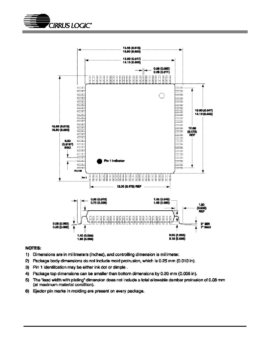
38
DS553PP1
5. 100-PIN MQFP PACKAGE SPECIFICATIONS (20X14X2.85mm)
0.310
±
0.050
A
0.650
±
0.150
3.300
(MAX)
1.600
±
0.150
DETAIL A
0.800
±
0.150
0~8
∞
0.150±0.008
20.000
±
0.100
23.200
±
0.250
100
31
50
81
1
14
.000
±
0.100
17.200
±
0.250
30
51
80
2.85
±
0.127
0.200
(MIN)
1.35
±
0.05
Figure 18. 100-Pin MQFP Package (20x14x2.85mm)
Note: Measurement Units = mm
CS7410
DS553PP1
39
6. 100-PIN LQFP PACKAGE SPECIFICATIONS (14X14X1.4mm)
Figure 19. 100-Pin LQFP Package (14X14X1.4mm)