| –≠–ª–µ–∫—Ç—Ä–æ–Ω–Ω—ã–π –∫–æ–º–ø–æ–Ω–µ–Ω—Ç: CS7620-IQ | –°–∫–∞—á–∞—Ç—å:  PDF PDF  ZIP ZIP |
Preliminary Product Information
This document contains information for a new product.
Cirrus Logic reserves the right to modify this product without notice.
1
Copyright
©
Cirrus Logic, Inc. 1999
(All Rights Reserved)
P.O. Box 17847, Austin, Texas 78760
(512) 445 7222 FAX: (512) 445 7581
http://www.cirrus.com
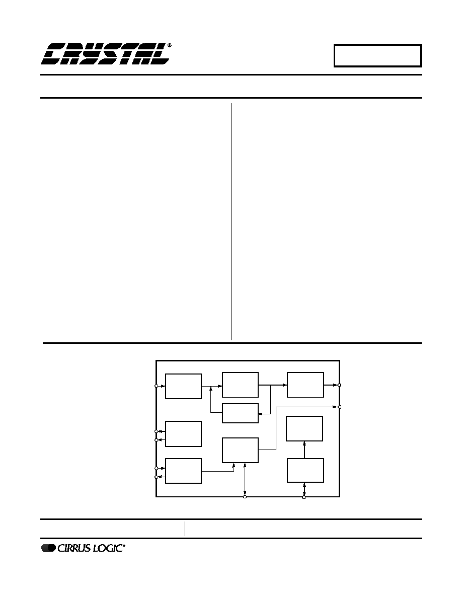
CS7620
CCD Imager Analog Processor
Features
l
13-Bit A/D Conversion Using DRXTM
Technology
l
Backlight Compensation
l
Supports three Input Ranges of 0.53V,
1.07V, and 1.60V
l
Multi-Sync CCD Timing Generator
l
High Resolution Output Mode
l
Low Resolution (Preview) Output Mode for
LCD Driver
l
Integrated Correlated Double Sampler
l
Digital Black Level Clamp
l
Digital Outputs Selectable for 13, 12, or 10 Bits
l
Two Integrated General Purpose DACs
l
Low Power Consumption
l
Power Down Mode
l
High Speed Serial Interface
l
Supports a Large Variety of Clock Input
Frequencies
l
Low power mode option
Description
The CS7620 is a low-power analog front-end processor
for interline or frame transfer CCD imagers. Main appli-
cations include digital still image cameras with up to
8k◊8k pixels.
The architecture includes a correlated double sampler,
black level clamp and a 13-bit A/D conversion module
using patented DRX technology. In addition, the chip
contains a timing generator, which supports common
CCDs from IBM, and Polaroid. For CCDs using different
timing signals, the internal timing generator can be
bypassed.
There are 2 general purpose DACs available which can
be used to drive motors for iris and shutter control.
Chip parameters can be programmed using a high
speed 4-wire asynchronous digital interface.
The chip outputs digitized CCD data in either 13-bit, 12-
bit or 10-bit format. 10-bit outputs are generated from the
13-bit A/D output by a programmable companding curve.
ORDERING INFORMATION
CS7620-IQ -40 to +85 ∞C 64-pin TQFP
10x10x1.4mm
CCD OUTPUT
MASTER
CDS/DRX
DATA OUT
PLL
OUTPUT
REGISTER
SERIAL
BLOCK
COMPANDER
A/D
CONVERTER
BLACK
LEVEL
TIMING
GENERATOR
CCD TIMING SIGNALS
CLOCK OUT
GAIN
CLOCK
INTERFACE
SERIAL BUS
DAC
2 DACS
OUTPUTS
CLOCK
JUL `99
DS301PP2

CS7620
2
DS301PP2
TABLE OF CONTENTS
1 CHARACTERISTICS/SPECIFICATIONS .................................................................................. 5
DIGITAL CHARACTERISTICS ................................................................................................. 5
POWER CONSUMPTION ........................................................................................................ 5
RECOMMENDED OPERATING CHARACTERISTICS............................................................ 5
ABSOLUTE MAXIMUM RATINGS ........................................................................................... 6
ADC (ANALOG-TO-DIGITAL CONVERTER) ........................................................................... 6
CDS/VGA PARAMETERS ........................................................................................................ 6
FREQUENCY SYNTHESIZER PARAMETERS ....................................................................... 6
SERIAL INTERFACE TIMING SPECIFICATIONS ................................................................... 7
2 GENERAL DESCRIPTION ........................................................................................................ 8
3 OPERATION .............................................................................................................................. 9
3.1 Black Level Adjustment .................................................................................................... 10
3.2 Gain Adjust Block ............................................................................................................. 12
3.3 13-to-10 Bit Compander ................................................................................................... 13
3.4 Timing Generator ............................................................................................................. 15
3.4.1 Vertical and Horizontal Timing Mode .................................................................. 15
3.4.2 Horizontal Only Timing Mode .............................................................................. 16
3.4.3 Slave mode ......................................................................................................... 17
3.4.4 Horizontal Timing Generator ............................................................................... 17
3.4.5 Vertical Timing Generator ................................................................................... 19
3.4.6 Frame Timing ...................................................................................................... 19
3.5 Frequency Synthesizer .................................................................................................... 19
3.6 8-Bit General Purpose DACs ........................................................................................... 20
3.7 Stand By Mode ................................................................................................................ 20
3.8 Preview Mode .................................................................................................................. 21
3.9 Serial Interface ................................................................................................................. 21
3.10 Recommended Register Settings .................................................................................. 21
4 REGISTER DESCRIPTIONS ................................................................................................... 25
4.1 Reset ................................................................................................................................ 28
4.2 Power Down Control 1 ...................................................................................................... 28
4.3 Power Down Control 2 ...................................................................................................... 29
4.4 Operation Control 1........................................................................................................... 29
4.5 Operation Control 2........................................................................................................... 31
4.6 Black Level Control - Accumulator (LSB).......................................................................... 32
4.7 Black Level Control - Accumulator (MSB)......................................................................... 32
4.8 General Black Level.......................................................................................................... 33
4.9 Black Level Control - Loop Gain, Clamp Length............................................................... 33
4.10 Gain Calibration - Offset 1 .............................................................................................. 34
4.11 Gain Calibration - Offset 2 .............................................................................................. 34
4.12 Gain Calibration - Offset 3 .............................................................................................. 35
Contacting Cirrus Logic Support
For a complete listing of Direct Sales, Distributor, and Sales Representative contacts, visit the Cirrus Logic web site at:
http://www.cirrus.com/corporate/contacts/
Preliminary product information describes products which are in production, but for which full characterization data is not yet available. Advance product infor-
mation describes products which are in development and subject to development changes. Cirrus Logic, Inc. has made best efforts to ensure that the information
contained in this document is accurate and reliable. However, the information is subject to change without notice and is provided "AS IS" without warranty of
any kind (express or implied). No responsibility is assumed by Cirrus Logic, Inc. for the use of this information, nor for infringements of patents or other rights
of third parties. This document is the property of Cirrus Logic, Inc. and implies no license under patents, copyrights, trademarks, or trade secrets. No part of
this publication may be copied, reproduced, stored in a retrieval system, or transmitted, in any form or by any means (electronic, mechanical, photographic, or
otherwise) without the prior written consent of Cirrus Logic, Inc. Items from any Cirrus Logic website or disk may be printed for use by the user. However, no
part of the printout or electronic files may be copied, reproduced, stored in a retrieval system, or transmitted, in any form or by any means (electronic, mechanical,
photographic, or otherwise) without the prior written consent of Cirrus Logic, Inc.Furthermore, no part of this publication may be used as a basis for manufacture
or sale of any items without the prior written consent of Cirrus Logic, Inc. The names of products of Cirrus Logic, Inc. or other vendors and suppliers appearing
in this document may be trademarks or service marks of their respective owners which may be registered in some jurisdictions. A list of Cirrus Logic, Inc. trade-
marks and service marks can be found at http://www.cirrus.com.

CS7620
DS301PP2
3
4.13 Timing Control - Number of Lines (MSBs)...................................................................... 36
4.14 Timing Control - Number of Lines (LSBs)....................................................................... 38
4.15 Timing Control - Number of Columns (MSBs) ................................................................ 38
4.16 Timing Control - Number of Columns (LSBs) ................................................................. 39
4.17 Timing Control - Number of Dark Rows.......................................................................... 39
4.18 Timing Control - Start of Black Pixels ............................................................................. 40
4.19 Timing Control - End of Black Pixels .............................................................................. 40
4.20 Timing Control - Number of Rows until Active ................................................................ 41
4.21 Timing Control - Start of Active Pixels ............................................................................ 42
4.22 Timing Control - Vertical Time Division .......................................................................... 42
4.23 Timing Control - Lines in Storage Buffer (MSBs) ........................................................... 43
4.24 Timing Control - Lines in Storage Buffer (LSBs) ............................................................ 43
4.25 Timing Control - Extra Lines of Exposure in Low Resolution Mode (MSBs) .................. 43
4.26 Timing Control - Extra Lines of Exposure in Low Resolution Mode (LSBs) ................... 44
4.27 Timing Control - Vsync Mode, Lines of Exposure in Low Resolution Mode (MSBs) ...... 44
4.28 Timing Control - Lines of Exposure in Low Resolution Mode (MSBs) ............................ 47
4.29 Timing Control - Polarity of Vertical Shift Outputs .......................................................... 47
4.30 Horizontal Timing Control - H1 ....................................................................................... 48
4.31 Horizontal Timing Control - H2 ....................................................................................... 49
4.32 Horizontal Timing Control - H3 ....................................................................................... 50
4.33 Horizontal Timing Control - H4 ....................................................................................... 51
4.34 Horizontal Timing Control - Analog Delays..................................................................... 52
4.35 Compander - Black Slope, Slopes (MSBs)..................................................................... 53
4.36 Compander - Slope 1 (LSBs) ......................................................................................... 53
4.37 Compander - Slope 2 (LSBs) ......................................................................................... 54
4.38 Compander - Slope 3 (LSBs) ......................................................................................... 54
4.39 Compander - Slope 4 (LSBs) ......................................................................................... 55
4.40 Compander - Offset 1 ..................................................................................................... 55
4.41 Compander - Offsets (MSBs) ......................................................................................... 56
4.42 Compander - Offset 2 (LSBs) ......................................................................................... 56
4.43 Compander - Offset 3 (LSBs) ......................................................................................... 57
4.44 Compander - Offset 4 (LSBs) ......................................................................................... 57
4.45 Compander - X1 (MSBs) ................................................................................................ 58
4.46 Compander - X1 (LSBs) ................................................................................................. 58
4.47 Compander - X2 (MSBs) ................................................................................................ 59
4.48 Compander - X2 (LSBs) ................................................................................................. 59
4.49 Compander - X3 (MSBs) ................................................................................................ 60
4.50 Compander - X3 (LSBs) ................................................................................................. 60
4.51 Power_up Counter.......................................................................................................... 61
4.52 Valid_data/Dout Edge/Clock_in Divider.......................................................................... 61
4.53 DAC #1 Control .............................................................................................................. 62
4.54 DAC #2 Control .............................................................................................................. 62
4.55 Device ID ........................................................................................................................ 63
4.56 Rev Code........................................................................................................................ 63
5 PIN DESCRIPTIONS ............................................................................................................... 64
5.1 Supply .............................................................................................................................. 65
5.2 Ground ............................................................................................................................. 65
5.3 CMOS Input ..................................................................................................................... 65
5.4 CMOS Analog Input ......................................................................................................... 66
5.5 CMOS Analog Output ...................................................................................................... 66
5.6 CMOS 4 mA Output ......................................................................................................... 66
5.7 CMOS 28 mA Output ....................................................................................................... 67
5.8 Misc ................................................................................................................................. 67
6 PACKAGE DIMENSIONS ....................................................................................................... 68

CS7620
4
DS301PP2
LIST OF FIGURES
Figure 1. SEN Timing ......................................................................................................................... 7
Figure 2. Serial Write Timing.............................................................................................................. 7
Figure 3. Read Data Timing ............................................................................................................... 7
Figure 4. Digital Camera Block Diagram ............................................................................................ 8
Figure 5. CS7620 Block Diagram....................................................................................................... 8
Figure 6. Idealized CCD output waveform ......................................................................................... 9
Figure 7. Transfer function of VGA circuit (assuming full scale level of 1.07V)................................ 10
Figure 8. Block diagram of CDS/VGA circuit .................................................................................... 10
Figure 9. Idealized timing diagram of VGA/CDS circuit.................................................................... 11
Figure 10. Black level adjustment loop............................................................................................. 11
Figure 11. Transfer function of Vin to Gain Adjust output Block (assuming full scale level of 1.07V)13
Figure 12. Gain Adjust output Block................................................................................................. 13
Figure 13. 13-to-10 bit compander ................................................................................................... 15
Figure 14. CS7620 output data and clocks ...................................................................................... 15
Figure 15. CS7620 output data and clocks ...................................................................................... 16
Figure 16. Picture Signal Timing ...................................................................................................... 16
Figure 17. Signal Timing for Horizontal Only Mode.......................................................................... 17
Figure 18. Signal Timing for Slave Mode ......................................................................................... 17
Figure 19. Detailed Signal Timing Showing Internal Clock Phases ................................................. 18
Figure 20. Default Timing of Horizontal Signals to the CCD ............................................................ 18
Figure 21. High Resolution Mode..................................................................................................... 20
Figure 22. Low Resolution Mode...................................................................................................... 20
Figure 23. Typical Connection Diagram Using Vertical and Horizontal Timing Mode ...................... 22
Figure 24. Typical Connection Diagram Using Horizontal Only Timing Mode ................................. 23
Figure 25. Typical Connection Diagram Using Slave Mode............................................................. 24
Figure 26. Transfer Function of Analog Input to Digital Output (assuming full scale level of 1.07V) 36
Figure 27. Transfer Function of ADC with Fixed Gain Settings (assuming full scale level of 1.07V) 37
Figure 28. Typical CCD Pixel Arrangement ..................................................................................... 41
Figure 29. 2 million pixel IBM CCD (5:1 reduction) .......................................................................... 46
Figure 30. 2 million pixel IBM CCD (5:1 reduction) RGB pattern ..................................................... 46
Figure 31. 1.3 million pixel IBM CCD (8:2 reduction) ....................................................................... 46
Figure 32. 1.3 million pixel IBM CCD (4:1 reduction) RGB pattern .................................................. 46
Figure 33. Vertical Timing Division for Low Resolution Mode .......................................................... 46
LIST OF TABLES
Table 1. Companding Operational Control....................................................................................... 14
Table 2. Default Phases for Horizontal Signal Edges ...................................................................... 18
Table 3. Different Resolution Operating Modes ............................................................................... 19
Table 4. General Purpose DAC specifications ................................................................................. 20
Table 5. IBM35CCD2PIX1 ............................................................................................................... 25
Table 6. IBM35CCD13PIX ............................................................................................................... 25
Table 7. Register Description ........................................................................................................... 25
Table 8. Different Resolution Operating Modes ............................................................................... 30
Table 9. Full Scale Level Choices .................................................................................................... 32
Table 10. Offset Range .................................................................................................................... 32
Table 11. Black Loop Time Constant ............................................................................................... 33
CS7620
DS301PP2
5
1
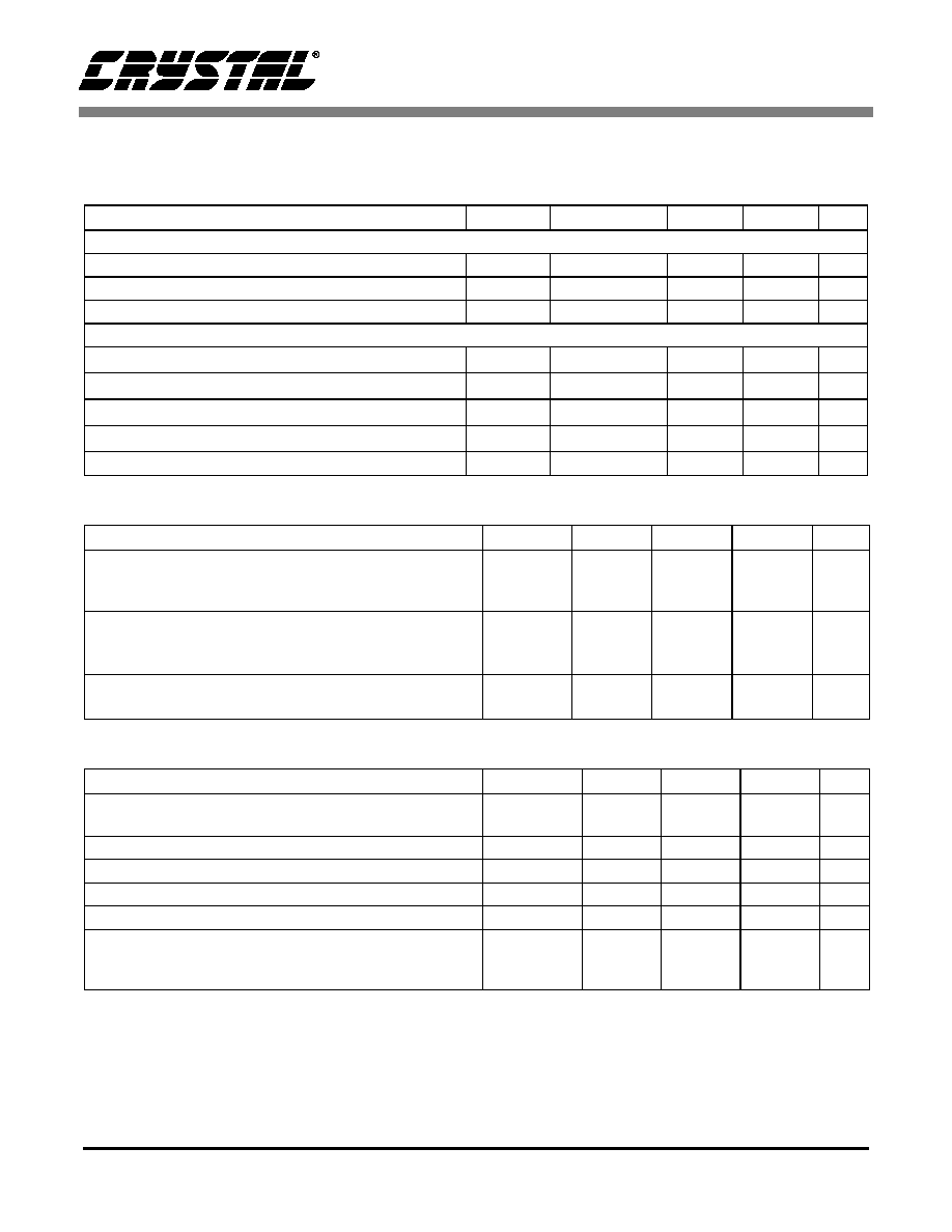
CHARACTERISTICS/SPECIFICATIONS
DIGITAL CHARACTERISTICS
(T
A
= 25 ∞ C; V
DD
_Ring = 5 V)
POWER CONSUMPTION
(T
A
= 25 ∞ C; V
AA
= V
DD
= 5 V; Output Load = 30 pF)
RECOMMENDED OPERATING CHARACTERISTICS
Parameter
Symbol
Min
Typ
Max
Units
Logic Inputs
High-Level Input Voltage
V
IH
V
DD
_Ring-0.8
-
-
V
Low-Level Input Voltage
V
IL
-
-
0.8
V
Input Leakage Current
I
IN
-
-
10
µ
A
Logic Outputs
High-Level Output Source Current @ I
OH
= 4mA
V
OH
V
DD
-0.4
-
V
Low-Level Output Sink Current @ I
OL
= 4mA
V
OL
-
-
0.4
V
(H1-H4) Output Source Current @ I
OH = 24mA
V
OH_HCLK
V
DD
-0.4
V
(H1-H4) Output Sink Current @ I
OL = 24 mA
V
OL_HCLK
0.4
V
3-State Leakage Current
I
OZ
-
-
10
µ
A
Parameter
Symbol
Min
Typ
Max
Units
Power Dissipation
Peak Mode
Preview Mode
Stand By Down
P
D
P
DLR
P
DPD
-
-
-
375
275
0.125
-
-
-
mW
mW
mW
Analog Power Supply Current
Peak Mode
Preview Mode
Stand By Down
I
AN
I
ALR
I
APD
-
-
-
60
40
0.025
-
-
-
mA
mA
mA
Digital Power Supply Current
Peak/Preview Mode
Stand By Mode
I
DN
I
DPD
-
-
15
0
-
-
mA
mA
Parameter
Symbol
Min
Typ
Max
Units
Power Supply Voltage
V
AA1
, V
AA2
,
V
DDD
4.5
5.0
5.5
V
Power Supply Voltage for Digital Pads
V
DD_Ring
3.0
3.3/5.0
5.5
V
Power Supply Voltage for Horizontal CCD Signal Outputs
V
AA3
3.0
3.3/5.0
5.5
V
GNDA to GNDD Voltage Differential
10
mV
Clock Frequency Range
8
160
MHz
Analog Full Scale Input Voltage Range
(w/ fs_lvl = 10)
(w/ fs_lvl = 01)
(w/ fs_lvl = 00)
A
IN
-
1.60
1.07
0.53
-
V
p-p

CS7620
6
DS301PP2
ABSOLUTE MAXIMUM RATINGS
WARNING: WARNING:Operation at or beyond these limits may result in permanent damage to the device.
Normal operation is not guaranteed at these extremes.
ADC (ANALOG-TO-DIGITAL CONVERTER)
CDS/VGA PARAMETERS
FREQUENCY SYNTHESIZER PARAMETERS
Parameter
Symbol
Min
Max
Units
Power Supply Voltage
V
AA1
, V
AA2
,
V
AA3
,
V
DD_Ring
,
V
DDD
-0.3
7.0
V
Digital Input Voltage
GNDD-0.3
V
DDD
+0.3
V
Analog Input Voltage
A
IN
GNDA-0.3
V
AAI
+0.3
V
Input Current
(except supply pins)
10
mA
Ambient Temperature Range
70
+70
∞C
Lead Solder Temperature (10sec duration)
+260
∞C
Storage Temperature Range
-65
+150
∞C
Parameter
Symbol
Min
Typ
Max
Unit
Input Voltage Range
(w/ fs_lvl = 10)
(w/ fs_lvl = 01)
(w/ fs_lvl = 00)
-
1.60
1.07
.53
-
V
0-p
ADC resolution
-
10
-
bits
Conversion Rate
Maximum
16
-
-
MHz
Total Differential Non-Linearity
-
±1
-
LSB
Total Integral Non-Linearity
-
±1
-
LSB
Parameter
Symbol
Min
Typ
Max
Unit
Input Voltage Range
(w/ fs_lvl = 10)
(w/ fs_lvl = 01)
(w/ fs_lvl = 00)
-
1.60
1.07
.53
-
V
0-p
Total Gain Range
A
VGA
-
18
-
dB
Input Referred Noise (rms)
Maximum Gain Setting
Vn
VGA
-
-
0.2
mV
Parameter
Symbol
Min
Typ
Max
Unit
CLKIN Frequency
F
clock_in
8 -
160
MHz
PLL Output Frequency
F
PLL_OUT
8 -
16
MHz
CLKIN Duty Cycle
D
clock_in
20
-
80
%
Output Jitter
-
200
-
ps
Duty Cycle
-
50
-
%
PLL Acquisition Time
-
200
-
µs
CS7620
DS301PP2
7
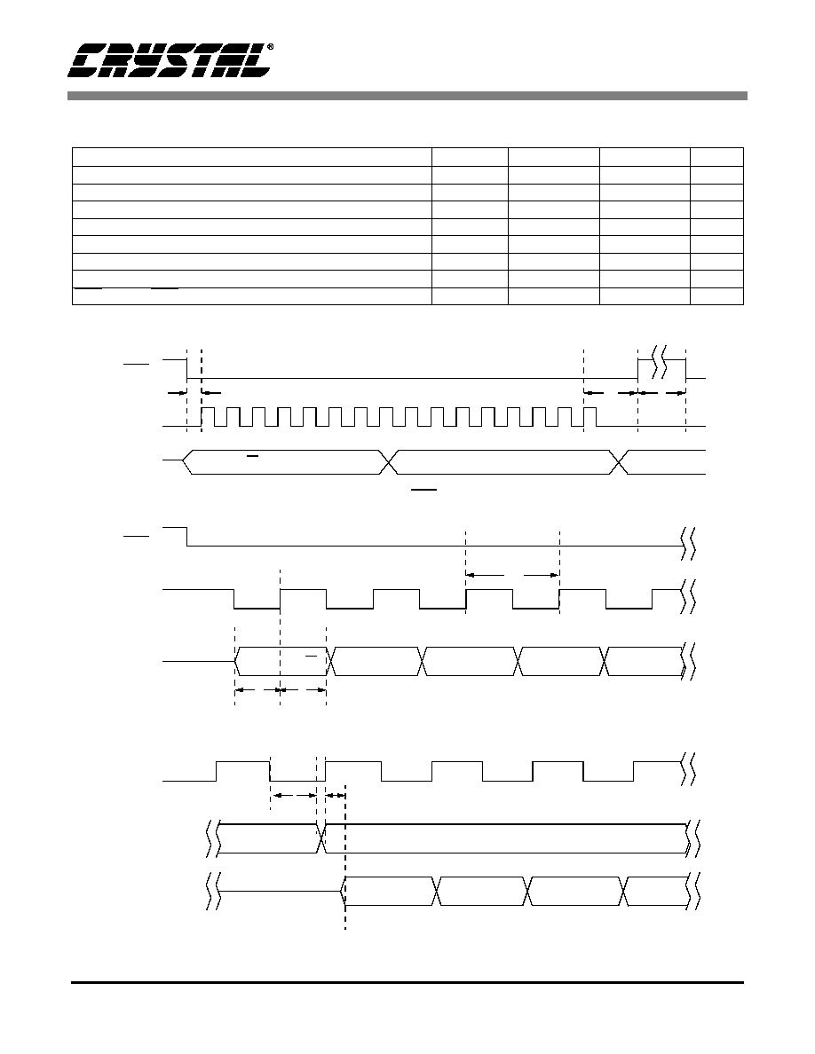
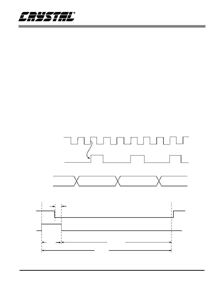
SERIAL INTERFACE TIMING SPECIFICATIONS
Notes: 1. the minimum serial clock period must be longer than two pixel clock periods.
Description
Symbol
Minimum
Maximum
Unit
Enable Setup
t1
10
-
ns
SDAT Setup
t2
10
-
ns
SDAT Hold
t3
10
-
ns
Serial Clock Period
(Note 1)
t4
143
-
ns
Write Data Invalid
t5
0
10
ns
Read Data Valid
t6
0
10
ns
Clock to Disable
t7
143
-
ns
SEN Rise to SEN Fall
t8
200
-
ns
Figure 1. SEN Timing
SCLK
SDATI
R/W, ADDR <6.0>
DATA <7.0>
t7
t8
t1
SEN
Figure 2. Serial Write Timing
SDATI
t4
SCLK
SEN
t2
t3
R/W
A6
A5
A6
A3
Figure 3. Read Data Timing
SCLK
A0
XX (DON'T CARE)
SDATI
t5
t6
D7
D6
D5
SDATO
CS7620
8
DS301PP2
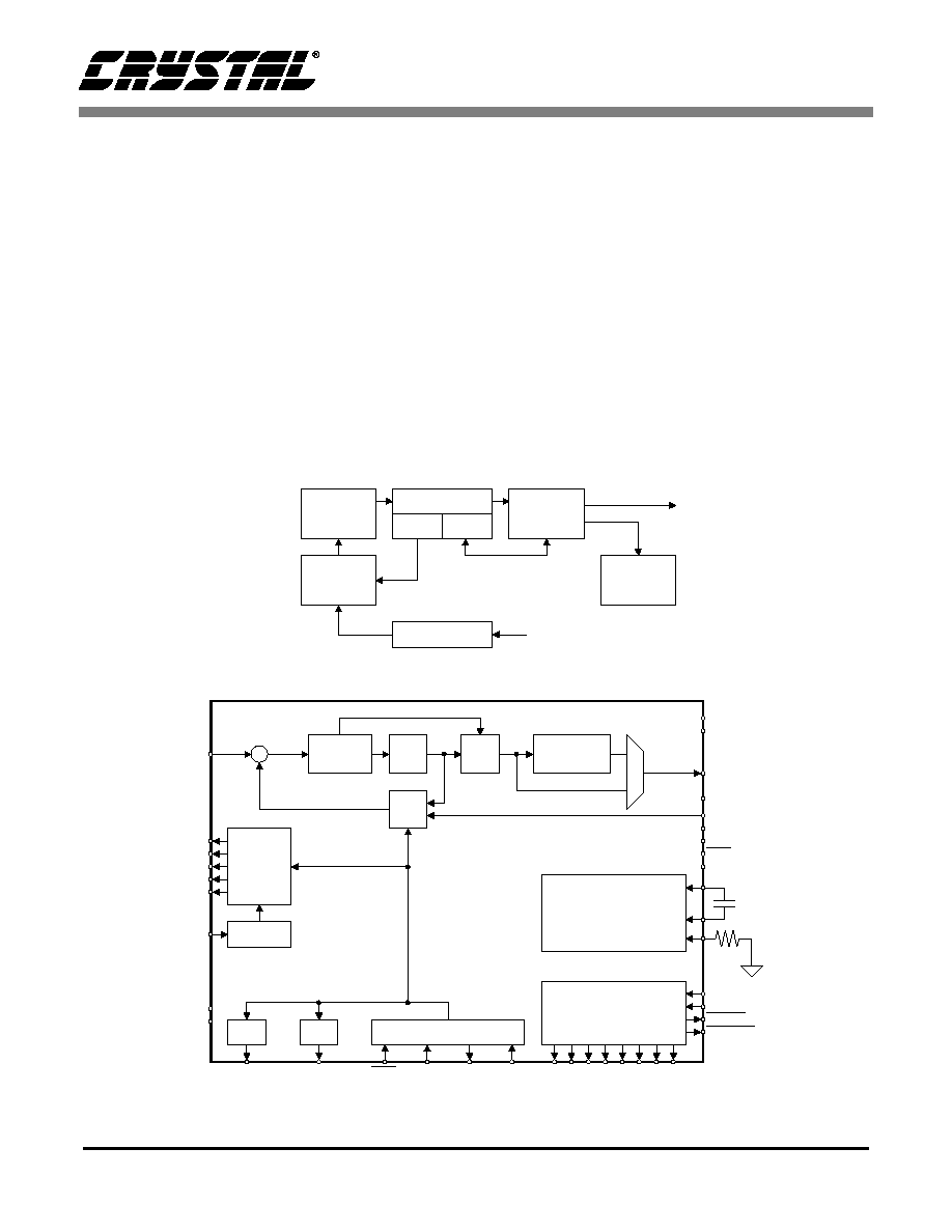
2 GENERAL DESCRIPTION
The CS7620 forms the heart of a four chip digital
CCD Camera. The four chips include the CCD im-
ager, the CS7620 CCD digitizer, a vertical drive in-
terface chip and a backend DSP chip to further
process the digital data (see Figure 4.) The CS7620
has a built-in timing generator which works with
imagers from IBM and Polaroid. If other CCDs are
used, the internal timing generator can be bypassed
and replaced by an external device, which outputs
the appropriate timing signals.
The patented DRX technology allows the CS7620
to output data with 13-bit dynamic range, and at the
same time reducing the power consumption to a 10-
bit equivalent A/D converter.
The digitized output is either available in 13-bits,
12-bits or 10-bits. The 10-bit output is created by
companding the 13-bit A/D output to 10-bits. The
companding curve consists of 4 linear segments,
where each slope and each start point is user pro-
grammable. Two output control signals and one
output clock provide synchronization with the out-
put data.
A block diagram of the CS7620 chip is shown in
Figure 5.
CCD
Vertical Drive
DC-DC converter
Backend
DSP
LCD Panel
Video Output
+5 V
+5 V to -5 V
CDS/ADC
Timing
Control
CS7620
Figure 4. Digital Camera Block Diagram
AIN
RG
H1
H2
H3
H4
CLOCK_IN
BYPASS_PLL
DIAG[1:0]
DAC_OUT1
DAC_OUT2
SEN
SDATI SDATO SCLK
V1 V2 V3 V4 S1 S2 S3 S4
RD_OUT
HSYNC
EXPOSE
LINE_ENA
BG_RES
REF_CAPN
REF_CAPP
TEST
RST
PWR_DN
SCAN_MODE
CLAMP
CLKO
DOUT[12:0]
(up to 3 may be unused)
GND[5]
VDD[5]
CDS/VGA
A/D
Gain
Adjust
13 to 10-bit
Compander
M
U
X
Black
Level
Analog
Clock
Generator
PLL
DAC1
DAC2
Serial Interface
Timing
Generator
Reference
1 µF
10 k
Figure 5. CS7620 Block Diagram

CS7620
DS301PP2
9
3 OPERATION
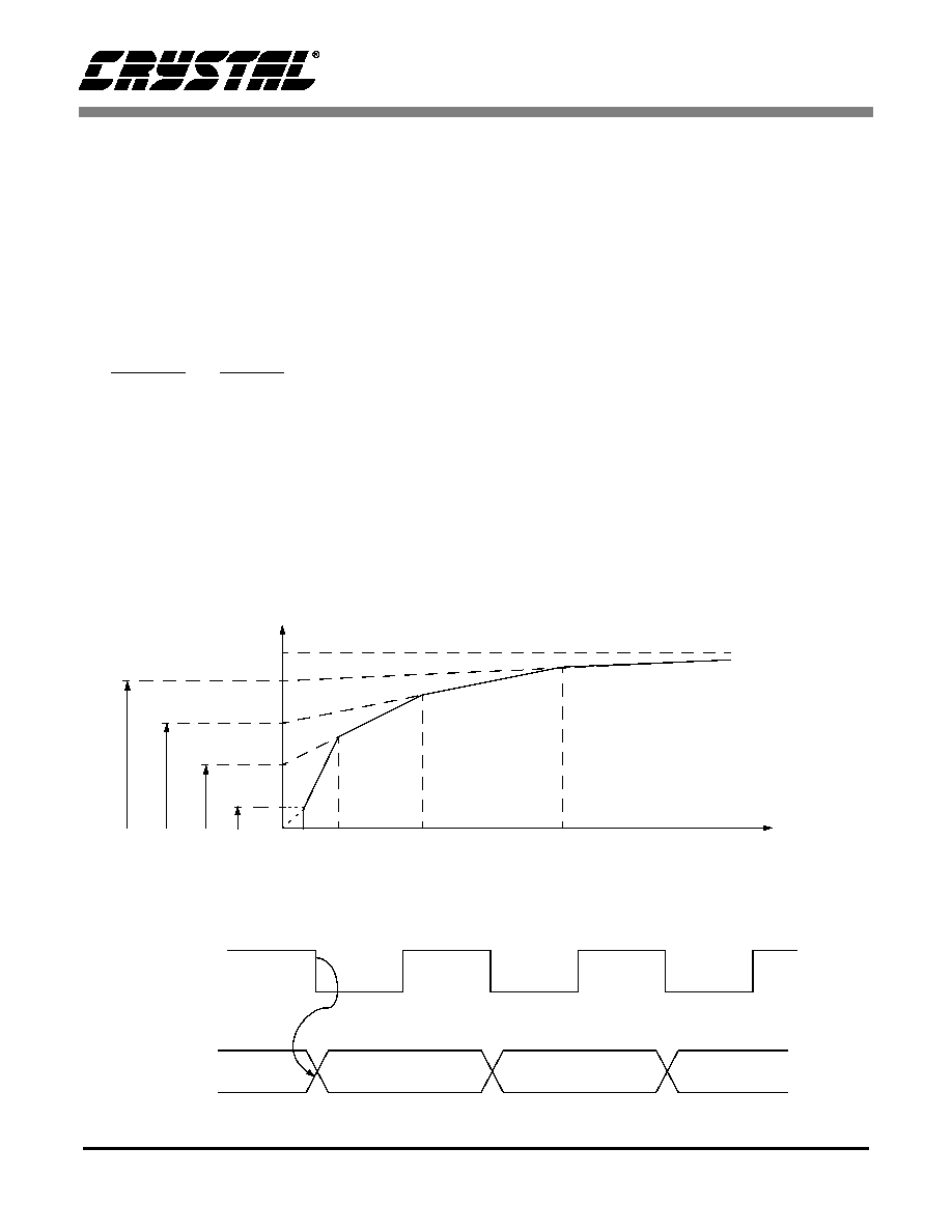
CDS/VGA (correlated double sampling/vari-
able gain amplification)
An idealized waveform of the CCD output is
shown in Figure 6.
The CCD output contains reset noise, thermal
noise, and 1/f noise generated in the CCD output
circuit. This degrades the S/N ratio and must be
cancelled. Since the noise during the active video
portion of the CCD signal is assumed to be corre-
lated with the noise during the feed through portion
of the signal, this noise can be cancelled by sub-
tracting the feed through level from the video level.
This operation is called correlated double sam-
pling. The active video signal is the difference be-
tween the feed through and video levels. The active
video signal varies according to light conditions. In
order to insure that the full dynamic range of the
ADC is utilized even under low light conditions,
the CCD output is amplified using a VGA. The
gain control is provided by a 2 bit control word
generated by an ADC after stage 1, which has a
gain of 1. Based on the input voltage, a gain of 1x,
2x, 4x, or 8x is subsequently applied to the signal.
The amount of gain is later adjusted in the digital
section. After the VGA, the signal gets digitized by
a 10 bit ADC. The 2 bit ADC output is used in
combination with the 10 bit ADC output to produce
a 13 bit output.
Adding more gain before the ADC does not offer
performance improvement because the noise of the
CCD (after gain is applied to it) begins to dominate
over the quantization noise. Any additional gain
should be done in digital since the performance is
the same as when the ADC output has the addition-
al gain applied.
In order to add more flexibility, the full scale input
range is programmable through register 07h. This
setting will determine what input level maps to the
highest ADC output code. Thus depending on the
saturation level of the particular CCD used in the
system, an appropriate full scale input level can be
chosen in the CS7620. The choices of full scale in-
put level are 1.6V, 1.07V, 0.53V with 1.07V the
default. In the remainder of this document, all the
figures and discussions assume a full scale level of
1.07 is used. If a different full scale level is used,
all the voltages scale up or down by x1.5 or x0.5 for
1.6V and 0.53V full scale levels respectively.
The transfer function of the VGA portion of the cir-
cuit is shown in Figure 7 with full scale level =
1.07. It is assumed that the CDS has already been
performed. If desired, the gain switching function-
ality can be disabled and forced to a fixed gain of
8x, 4x, 2x, or 1x. This way any dynamic range en-
hancement is lost and the digital output is only 10
bits. If a fixed gain of 1x is selected, DOUT[12:3]
is used as the output, a fixed gain of 2x will use
DOUT[11:2], etc. In order to use this mode, the
RESET LEVEL
FEED THROUGH
LEVEL
VIDEO LEVEL
PIXEL PERIOD
Figure 6. Idealized CCD output waveform
DARK
MAX. BRIGHTNESS
VIDEO
RANGE
SIGNAL
CS7620
10
DS301PP2
fixed gain register (16h) should be set and the cali-
bration offset registers (10h - 12h) should be set to
0.
The CDS/VGA circuit is composed of three stages.
The first stage has a fixed gain of 1, and the second
and third stages have variable gain with a combined
gain range of 1 to 8 (0-18 dB). Figure 8 shows a
block diagram of the CDS/VGA circuit. The total
gain is A = (C2/C3)(C4/C5) which is adjusted by
varying C3 and C5. The capacitor Cb on the front
of stage 1 is for black level adjustment and will be
discussed in detail later.
This circuit utilizes a two phase non-overlapping
clock to perform the desired CDS function. The
two phase clock also allows the video signal to be
passed to the output while retaining a positive po-
larity signal. Figure 9 shows a timing diagram of
the two phase clock along with the CCD signal and
output signals of stages one, two and three.
There is an internal mid-scale DC bias level circuit
at the input pin. This allows AC coupling into the
CS7620 with a capacitor and having the input auto-
matically biased to mid-supply without worrying
about external circuitry to perform this task.
3.1
Black Level Adjustment
In order to maintain a constant reference level for
black pixels, a feedback loop is implemented that
VOUT (V)
VIN (V)
1.07
0.53
0.27
0.13
1.07
0.5
1X
2X
4X
8X
ADC OUTPUT
00
01
10
11
Figure 7. Transfer function of VGA circuit (assuming full scale level of 1.07V)
-A2
-A3
C2
C3
C4
C5
1
2
STAGE 2
STAGE 3
VOUT
Vo1
-A1
C1
C1
1
VIN
ADC
Vo2
STAGE 1
CONTROLS C3, C5
CONTROLS GAIN ADJUST BLOCK IN DIGITAL
2
Cb
VREF
TO AOUT CIRCUITRY
Figure 8. Block diagram of CDS/VGA circuit
100 K
100 K
CS7620
DS301PP2
11
sets the black level value at the output of the ADC
to 64 in the 13 bit digital code. This loop is active
during the optically black pixels which are output
at the beginning and end of a frame as well as dur-
ing a portion of the horizontal blanking period. The
presence of black pixels in the CCD output is indi-
cated by the CLAMP pulse, which can either be
supplied externally or generated internally if the
timing for the CCD is generated by the CS7620.
The black level can also be written to through the
serial port.
In order to acquire a starting value for the black lev-
el, the loop will run over the several lines of black
pixels at the beginning of the frame. The block di-
agram of the loop is shown in Figure 10. The up-
date rate is once per line during active pixel lines,
and once every (n + 10) pixels during the optical
black lines.
CCD
INPUT
SIGNAL
1
2
OUT OF
STAGE 1
OUT OF
STAGE 2
OUT OF
STAGE 3
Figure 9. Idealized timing diagram of VGA/CDS circuit
V(1)
V(2)
V(3)
V(1)
V(2)
V(3)
V(1)
V(2)
V(3)
V(1)
V(2)
ADC
Z
-1
+
+
10
7
9
DAC
BINARY
TO
THERM
Z
-1
F
U
F
P
F
U
= UPDATE FREQUENCY
F
P
= PIXEL FREQUENCY
K
CLIP
CDS/VGA
VIN
FROM SERIAL INTERFACE
MUX
+
BLK LVL LOOP
`64'
Figure 10. Black level adjustment loop
-
GAIN REG

CS7620
12
DS301PP2
The open-loop transfer function of the black level
adjustment loop is
blk_gain = 1, 2, 4, or 8
where blk_gain is programmable through a register
and n = # of black pixels during clamp time, which
is also programmable. The value of Kxn will deter-
mine the open-loop gain of the system. The settling
time for the loop can be calculated using the fol-
lowing formula:
For offset range=1 (reg 06h, bit 0)
For offset range =0
During fixed gain mode the time constant is a little
different.
In order to achieve no ringing in the settling use,
for offset range = 1, and
for offset
range = 0.
The 9 MSBs of the black level accumulator can be
read or written through a register. If written, the
LSBs are set to zero. The black level is set to "8" in
a 10-bit digital output representation. In a 13-bit
representation, it is set to "64." The power-up de-
fault value in the accumulator is at mid level.
Also note that the black level adjust loop can be
disabled. In addition, the black level can be pro-
grammed through the serial port.
3.2
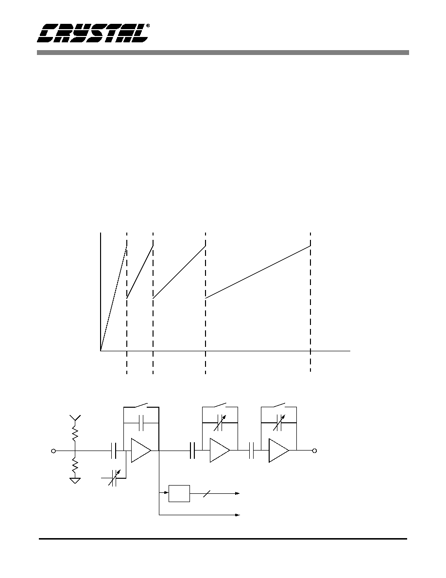
Gain Adjust Block
In order to increase the dynamic range of the ADC,
a variable gain, whose value is determined by the
signal level, is applied to each pixel. This allows
for 13 bits of dynamic range and 10 bits of resolu-
tion after accounting for the significance of the
ADC output bits. The gain applied in the analog is
illustrated in the transfer curve in Figure 7. Once
the signal is digitized, the gain adjust block uses the
gain information for a given pixel word and shifts
its bits accordingly. For example, using the default
full scale level of 1.07V, if Vin = 0.3 V, the VGA
would choose a gain of 2X so the ADC input is 0.6
V. The 10-bit output of the ADC (with no black
level) is (0.6/1.07) ◊ 1024 = 574, or "1000111110."
in binary. The gain adjust block will take this value
For a fixed gain of 1:
For a fixed gain of 2:
H z
( )
K
n
◊
z
1
≠
-------------
=
K
1
256
---------blk_gain
=
1
1
nK
≠
(
)
ln
---------------------------
≠
1
fu
-----
=
1
1
nK
2
-------
≠
ln
----------------------------
≠
1
fu
-----
=
1
1
nK
8
-------
≠
ln
----------------------------
≠
1
fu
-----
=
1
1
nK
4
-------
≠
ln
----------------------------
≠
1
fu
-----
=
For a fixed gain of 4:
For a fixed gain of 8:
1
1
nK
2
-------
≠
ln
----------------------------
≠
1
fu
-----
=
1
1
nK
≠
(
)
ln
---------------------------
≠
1
fu
-----
=
n
K
----
1
n
2K
-------
1
CS7620
DS301PP2
13
plus the bits representing the 2x gain and divide the
output by two (shift right by 1). The output of the
gain adjust block is then "0100011111.000." Note
that the decimal point is virtual, having no exist-
ence in silicon. It is representing the fact that we
keep 3 extra bits of lower significance in the output.
In the same manner, if Vin = 0.75 V, a gain of 1X
would be chosen and the output of the gain adjust
block would be "1011001101000." The transfer
function of the Vin/gain adjust out is shown in
Figure 11.
A block diagram of the gain adjust block is shown
in Figure 12.
Since the analog gain changes do not match the
digital shifts exactly, there is a potential to have
non-monotonic digital output. In order to remove
this problem, calibration is performed. During cal-
ibration, offset values are found that will be used to
counteract the errors caused by the analog gain
mismatch. Using these offset values, the final out-
put is a monotonic continuous 13-bit value.
3.3
13-to-10 Bit Compander
While a 13 bit output may be useful in some appli-
cations, others may require the standard 10 bit out-
put. To accommodate this and yet still retain the
advantages of the increased dynamic range, a 13-
to-10 (or 13-to-12) bit compander is included. By
DIG ADJUST OUT (13 BITS)
VIN (V)
1.07
0.53
0.27
0.13
8192
4096
1X
2X
4X
8X
ADC OUTPUT
00
01
10
11
1024
2048
0
Figure 11. Transfer function of Vin to Gain Adjust output Block (assuming full scale level of 1.07V)
GAIN ADJUST
SHIFT BY 0,1,2, OR 3
ADC OUTPUT
10
2
VGA_ADC OUTPUT
TO DIGITAL GAIN
13
Figure 12. Gain Adjust output Block
CS7620
14
DS301PP2
using the picture content as a guide, the user can se-
lect which curve will lead to the best overall dy-
namic range in the picture. The Companding
module takes 13-bit data as input, and outputs ei-
ther 10-bit companded data, 12-bit MSB-clipped
data or it lets the original 13-bit data pass through.
By programming the compander in the way that is
shown in Figure 13, it is possible to compensate for
backlighting conditions. Details in dark areas stay
visible, even in very complex lighting conditions.
These three modes can be selected through 2 regis-
ter bits in operational control.
In the 12-bit clipped mode, any input above 4095
gets clipped to 4095. In the 10-bit companded
mode, the input gets companded through a four
segment, three knees, fully programmable curve.
To program the curve, the placement of the three
knees in the companding curve must be deter-
mined. The next step is to determine the slope of
the four segments created by the three knees (slope
for each segment is defined as delta y / delta x). Fi-
nally, offsets must be calculated to keep the com-
panding curve continuous.
A fourth knee exists in the curve, which represents
the black level value. There are two options for the
10-bit black value. In case one, a linear mapping is
employed such that "blacker-than-black" pixel in-
formation is kept, with black (code 64 in the 13 bit
data) being defined as code 8 in the 10 bit domain.
The second option clips all pixel values less than
black (code 64 in the 13 bit data) to a programma-
ble offset value, offset1. This may be set to 0 if de-
sired. This option will lose the "blacker-than-
black" pixel information, but allow for slightly
more dynamic range. Note: If using the linear mode
(option 1), offset1 must be set to 8.
Registers x1 through x3 should be programmed
with the x coordinates of each one of the three
knees.
Registers slope1 through slope4 should be pro-
grammed with 256 multiplied by the calculated
slopes.
Finally, the offsets can be programmed following
the formulas below:
y1 = slope1/256 ◊ (x1-64) + offset1
y2 = slope2/256 ◊ (x2-x1) + y1
y3 = slope3/256 ◊ (x3-x2) + y2
offset2 = y1 - (x1 ◊ slope2 / 256)
offset3 = y2 - (x2 ◊ slope3 / 256)
offset4 = y3 - (x3 ◊ slope4 / 256)
(use integer division and discard the remainder)
When using the 10 bit companded output, be aware
of the non-linearity of the output data. If linear out-
put is needed to perform AWB or AGC, a linear
curve can be implemented to gather statistics. This
can be achieved by writing 8191 to x1 (set register
38h to 1fh and set register 39h to ffh) and setting
slope1 to 32 (set register 2eh to 00010xxxb and set
register 2fh to 20h). Once the statistics have been
gathered, all four registers should be returned to
their previous values before taking the actual pic-
ture.
Bits_out register bits
Output mode
0x
10 bits companded
10
13 bits
11
12 bits (clipped)
Table 1. Companding Operational Control
CS7620
DS301PP2
15
The output of the compander is available at the pins
DOUT<9:0> and it makes transitions either at the
falling or rising edges of the pixel rate clock CL-
KO, controlled by a register bit. The Falling edge
option is shown in Figure 14.
Two options exist for outputting data. The first op-
tion will output the pixel rate clock on the CLKO
pin. The polarity of the pixel clock out of the pin is
programmable so that the user may choose the ap-
propriate clock edge to latch in the data. Based on
the RD_OUT and HSYNC signals, the user will be
able to determine when he is over active pixels. The
second option will output a data_valid signal on the
CLKO pin that is synchronous with the input clock
(Figure 15). The data_valid signal will only toggle
over active pixels. The user may then latch the data
during this valid time. Note: DATA_VALID mode
cannot be used if the system clock runs at the pixel
rate.
3.4
Timing Generator
There are three timing options available with the
CS7620. The chip may produce all the vertical and
horizontal timing for the imager, only the horizon-
tal timing, or the chip may be used in a complete
slave mode and not produce any of the CCD timing
at all. Each will be discussed in detail in this sec-
tion.
3.4.1
Vertical and Horizontal Timing
Mode
To select this option, the user must tie the
BYPASS_PLL pin low and select the proper inter-
nal timing mode in the timing mode register. The
CS7620 is the master of the clocking. It will pro-
vide vertical outputs and horizontal outputs. In this
mode, the user must control two signals. The first is
the master PWR_DN signal. When this signal is
high, all of the CS7620 powers down except for the
1023
CODE_IN
CODE_OUT
8191
X1 X2
X3
SLOPE1
SLOPE2
SLOPE3
SLOPE4
OFFSET2
OFFSET3
OFFSET4
OFFSET1
64
(x2,y2)
(x1,y1)
(x3,y3)
Figure 13. 13-to-10 bit compander
Figure 14. CS7620 output data and clocks
CLKO
DOUT<9:0>
CS7620
16
DS301PP2
DAC outputs (these may be powered down through
register control if they are not being used). The sec-
ond signal is the EXPOSE signal. This signal
should go high at the beginning of exposure and
low at the beginning of readout. The suggested tim-
ing of these signals is shown in Figure 16. Note that
the chip must power up at least 500 µs before read-
out begins. The LINE_ENA and CLAMP pins are
not used in this mode.
3.4.2
Horizontal Only Timing Mode
To select this mode, the user must set the
BYPASS_PLL pin low and select external timing
mode in the timing mode register. The CS7620 is
the master of the pixel rate timing, but the line and
frame timing is controlled externally. In this mode,
the user must control four signals- PWR_DN, EX-
POSE, LINE_ENA, and CLAMP. The master
PWR_DN signal may be used to conserve power
during non-readout time. The EXPOSE pin is rede-
fined as the non-readout signal. When high, the
H1-H4 and RG signals are set in their idle state
(low for H1-H4, high for RG). The LINE-ENA pin
should be high during the vertical shift and load pe-
riods. This will hold the H1-H4 signals in their
user-programmable default states. The CLAMP
pin should be high when over dark reference
(black) pixels. The suggested timing for these sig-
nals is shown in Figure 17. Note that the chip
should power up at least 500 µs before the begin-
ning of readout. The CLAMP signal may also be
high during the dark pixel lines at the beginning of
the frame.
Figure 15. CS7620 output data and clocks
CLKO (DATA_VALID)
DOUT<9:0>
SYSTEM_CLK
T
FRAME
T
EXP
T
READOUT
EXPOSE SIGNAL
Figure 16. Picture Signal Timing
WARNING: NOTE: It is recommended to keep the part in power down mode while not in use to reduce power
POWERDOWN SIGNAL
>500 µs

CS7620
DS301PP2
17
3.4.3
Slave mode
To select this mode, the user must set the
BYPASS_PLL pin high and select external timing
mode in the timing register. The CS7620 timing is
now slaved off of an external source and supplied
with sampling clocks for feedthrough and data. In
this mode, the user must control five signals-
PWR_DN, EXPOSE, CLAMP, CK_FT
(CLOCK_IN), and CK_DT (LINE_ENA). The
master PWR_DN signal may be used to conserve
power during non-readout time. The EXPOSE pin
is redefined as the non-readout signal. Using the
falling edge of this signal, the chip will delay its
RD_OUT pin output by the appropriate amount as
determined by the chip latency so that it will go ac-
tive at the correct point in the data stream. CLAMP
should be high when over the dark reference pixels.
The CLOCK_IN and LINE_ENA pins are rede-
fined as the CK_FT and CK_DT signals, which
sample the feedthrough and data levels, respective-
ly. The suggested timing for PWR_DN, EXPOSE,
and CLAMP is the same as shown previously in
Figures 16 and 17. The timing for CK_FT
(CLOCK-IN) and CK_DT (LINE-ENA) is shown
in Figure 18.
3.4.4
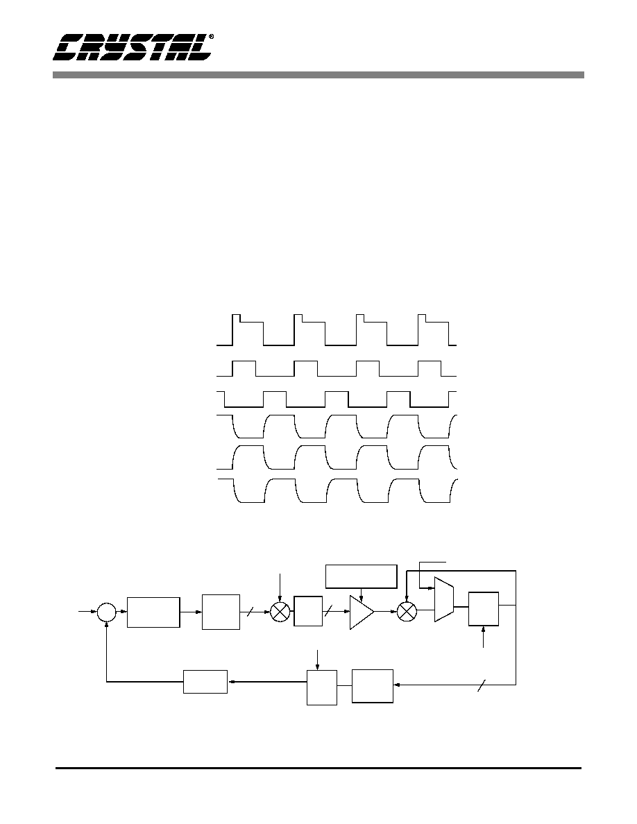
Horizontal Timing Generator
During every horizontal line period the data from
the horizontal shift register is shifted out on the
CCD output pin one pixel at a time. The analog tim-
ing generator creates the required driving signals to
control the CCD horizontal timing as well as the
analog sampling signals. The timing signals in-
volved in this operation are H1, H2, H3, H4 and
RG. The exact timing of these signals can be con-
T
LINE
CLAMP
LINE_ENA SIGNAL
SIGNAL
EXTENDED
PIXELS
DARK
PIXELS
ACTIVE
V SHIFT
& LOAD
T
LINE+1
Figure 17. Signal Timing for Horizontal Only Mode
PIXELS
ACTIVE
PIXELS
V SHIFT
& LOAD
CCD
INPUT
SIGNAL
CK_DT
CK_FT
Figure 18. Signal Timing for Slave Mode

CS7620
18
DS301PP2
trolled through the serial interface as described be-
low.
The pixel period is broken down into 8 equal time
periods. By delaying the clock a given number of
these time periods, different phases are created.
This is shown in Figure 19. These clock phases are
labeled t0-t7 and are shown relative to an idealized
CCD signal and the internal sampling signals.
Using these eight clock phases, the user may set the
rising and falling edges of each horizontal pixel
clock at 1/8 of a pixel clock period. In addition, the
user may set each horizontal signal to a default
state when the output lines are to be held constant
during blanking. The default timing for the hori-
zontal signals is shown in Figure 20 and Table 2.
See the register listing for more details.
Ideal
CCD Signal
CK_FT
CK_DT
internal
sampling
clocks
Figure 19. Detailed Signal Timing Showing Internal Clock Phases
H2
H3
H1
H4
RG
t0
t4 t5 t6 t7
t0
t3 t4 t5 t6 t7
t1 t2
t3
t1 t2
Ideal
CCD Signal
default
settings
Figure 20. Default Timing of Horizontal Signals to the CCD
Signal
Rising edge
Falling edge
Hold level
H1
t0
t5
high (`1')
H2
t2
t7
high (`1')
H3
t4
t1
high (`1')
H4
t6
t3
low (`0')
Table 2. Default Phases for Horizontal Signal Edges
CS7620
DS301PP2
19
3.4.5
Vertical Timing Generator
The signals involved in the vertical timing genera-
tor are the vertical shift clocks V1 through V4 and
the storage clocks S1 through S4. The vertical tim-
ing generator generates the signals needed by the
CCD to shift charge vertically down into the hori-
zontal shift register. The chip is the timing master,
and it generates the signals needed by the horizon-
tal timing generator and other modules to operate.
The timing generator is controlled externally by
various signals; the falling edge of the input signal
EXPOSE sets the part into readout mode, and after
this edge, it generates the timing signals to output a
full frame, provided that RST and PWR_DN are
not active.
The mode register selects the CCD timing, and the
resolution mode to be generated. Please refer to
IBM-CCD datasheet for more info.
The timing module's functionality can be config-
ured through the use of registers. Note that before
entering a preview mode, all of the programmable
parameters must be set prior to this.
Shiftl_num is the number of lines in the shift buff-
er.
Tdv is the length of the minimum vertical timing
interval measured in pixel clocks.
Num_pixels is the number of pixels per line
Num_lines is the number of lines per frame.
V_polarity allows to switch the polarity of all the
vertical timing signals going to the CCD.
Blk_begin is the first black pixel in a line
Blk_end is the last black pixel in a line
Drk_rws_fst is the number of black lines to be
readout at the beginning of the frame
Drk_rws_lst is the number of black lines to be
readout at the end of the frame
3.4.6
Frame Timing
Figures 21 and 22 illustrates the frame timing for
the low and high resolution modes.
HSYNC is high during the active pixel area, and it
is low during vertical shift (horizontal and vertical
blanking periods).
RD_OUT is triggered by the falling edge of ex-
pose, it is delayed by the chip latency, and it
switches back high once the last pixel has been read
out of the CS7620. RD_OUT is low during the ac-
tive pixel areas and during the horizontal blanking
periods (vertical line shifts) and it goes high during
the vertical blanking period, between frames.
The dotted lines in Figures 21 and 22 correspond to
the vsync option which can be enabled by writing a
one to register vsync_md (register 25h bit 5). This
causes the RD_OUT signal to behave like a vertical
sync signal. It makes the signals HSYNC and
RD_OUT the same length at the beginning of a
new frame (see Figures 21 and 22).
3.5
Frequency Synthesizer
Since multiple clock phases and timing are re-
quired for the pixel rate clocks controlling the CCD
imager, the clock generator contains a PLL circuit
to generate the proper timing. "Frequency Synthe-
sizer Parameters" on page 6 shows the require-
ments for this PLL. The frequency of the input
clock may be set from 1 to 20X the pixel clk fre-
quency, in integer multiples. The frequency used is
Mode value
Mode
000
IBM35CCD2PIX1 and IBM35CCDPIX13
CCD high resolution mode
001
IBM35CCD2PIX1 CCD low resolution
(viewfinder) mode
010-100
reserved
101
IBM35CCD13PIX CCD (2x2) low resolu-
tion (viewfinder) mode
110
IBM35CCD13PIX CCD (3x4) low resolu-
tion (viewfinder) mode
111
external timing used
Table 3. Different Resolution Operating Modes

CS7620
20
DS301PP2
register programmable in terms of multiples of the
pixel clock rate.
3.6
8-Bit General Purpose DACs
Two 8-bit current-output DACs are available for
external use. Table 4 shows the output specifica-
tions of these DACs.
3.7
Stand By Mode
Stand-by mode can be entered using the PWR_DN
pin. All circuitry on chip including the DACs can
be powered down. Various functional blocks can
be powered down individually, and are controlled
through registers. Note that the DACs can be pow-
ered down in that way if not in use. During Stand
By mode, the register contents are maintained and
Expose
RD_OUT
HSYNC
V1 ... V4
H1 ... H4
S1 ... S4
vsync_md = 1
vsync_md = 0
262 lines
first read-out line
last read-out line
Figure 21. High Resolution Mode
Expose
RD_OUT
HSYNC
V1 ... V4
H1 ... H4
S1 ... S4
vsync_md = 1
vsync_md = 0
262 lines
first read-out line
last read-out line
don't care
262 lines
first read-out line
picture n
picture n
picture (n+1)
Figure 22. Low Resolution Mode
Parameter
High impedance
mode
Low impedance
mode
Iout
2.155 mA
8.7 mA
loading
464
115
Table 4. General Purpose DAC specifications

CS7620
DS301PP2
21
do not have to be reprogrammed at the next power
up.
3.8
Preview Mode
It is strongly recommend that the chip should be
kept in Stand By mode when not in use in order to
save power. When in preview mode, a user may
wish to cut down the resolution of the ADC output
to 6 bits in order to reduce the power consumption
of the CS7620. In this mode, the current is reduced
by 20 mA. With the DRX (Dynamic Range eXten-
sion) circuitry, 3 bits of dynamic range are added to
the 6-bit ADC output producing a 9-bit output. The
pins DOUT[12:4] are used to output the digitized
data in preview or Stand By mode.
3.9
Serial Interface
The serial interface is designed to allow high speed
input to control the chip's registers. The specifica-
tions on this interface are as follows:
Asserting the enable pin, SEN, enables the serial
interface to perform data transfers. Data present on
the SDATI pin is latched into the CS7620 on each
rising edge of the serial clock, SCLK. Data output
on SDATO from the CS7620 is clocked out on the
rising edge of SCLK.
The CS7620 receives only the first 16 rising edges
of the SCLK while SEN is low and then ignores
any remaining SCLK and SDATI information. If
SEN goes high before 16 SCLK pulses have been
received, the CS7620 aborts the serial transfer.
The first bit is the R/W bit. R/W = 1 identifies the
transfer as a read. If (0), the transfer is a write. The
next seven bits define the address. For write trans-
fers, the second byte of the 16-bit packet contains
the data byte. For read transfers, the CS7620 out-
puts the read data on SDATO after accepting the
address. Address and data are transferred MSB
first. When not reading out data, the SDATO pin is
not driven by the chip (Hi-Z state).
The timing diagrams and specifications are shown
in "Serial Interface Timing Specifications" on
page 7 and Figures "SEN Timing", "Read Data
Timing", and "Serial Write Timing" on page 7.
3.10
Recommended Register Settings
These are the values that need to be written to the
registers to change the configuration of the CS7620
to work with each CCD in either low resolution or
high resolution mode. (2 ◊ 2) refers to a RGRGRG
pattern and (3 ◊ 4) refers to a RGBRGB pattern
CCD.

CS7620
22
DS301PP2
2.0M pixel (default)
high resolution
2.0M pixel (2x2)
low resolution
2.0M pixel (3x4)
low resolution
tim_modes(06h)
000b
001b
001b
num_lines[12:8](17h)
05h
05h
05h
num_lines[7:0](18h)
1Ch
1Ch
1Ch
num_pixels[12:8](19h)
06h
06h
06h
num_pixels[7:0](1Ah)
93h
93h
93h
drk_rws (frst/lst)(1Bh)
A4h
20h
20h
blk_begin(1Ch)
04h
04h
04h
blk_end(1Dh)
3Fh
3Fh
3Fh
act_rws (frst/lst)(1Eh)
B6h
32h
32h
act_begin(1Fh)
4Bh
4Bh
4Bh
tdv(20h)
01h
01h
01h
shiftl_num[8](21h)
01h
01h
01h
shiftl_num[7:0](22h)
06h
06h
06h
lowres_sen[3:0](25h)
XXXXb
0000b
0100b 2x sens
0001b 2x sens
0101b 3x sens
0000b
0010b 2x sens
Table 5. IBM35CCD2PIX1
1.3M pixel
high resolution
1.3M pixel (2x2)
low resolution
1.3M pixel (3x4)
low resolution
tim_modes(06h)
000b
101b
110b
num_lines[12:8](17h)
04h
04h
04h
num_lines[7:0](18h)
1Ch
1Ch
1Ch
num_pixels[12:8](19h)
05h
05h
05h
num_pixels[7:0](1Ah)
50h
50h
50h
drk_rws (frst/lst)(1Bh)
A4h
20h
20h
blk_begin(1Ch)
04h
04h
04h
blk_end(1Dh)
3Fh
3Fh
3Fh
act_rws (frst/lst)(1Eh)
B6h
42h
42h
act_begin(1Fh)
4Bh
4Bh
4Bh
tdv(20h)
01h
01h
01h
shiftl_num[8](21h)
01h
01h
01h
shiftl_num[7:0](22h)
06h
06h
06h
lowres_sen[3:0](25h)
XXXXb
0000b
0100b 2x sens
0000b
0010b 2x sens
Table 6. IBM35CCD13PIX
CS7620
DS301PP2
23
60.4 k
10 k
464
60.4 k
10 k
464
Substrate
Voltage
to CCD
to CCD
10 k
±1%
1 µF
Vertical
Drivers
to Microcontroller
to CCD
to CCD
1000 pF
100 k
VCC
VAA
CLK_IN
RESET
from
Microcontroller
from
CCD
NC
NC
XTAL_IN
BYPASS_PLL
RST
DIAG0
DIAG1
SCAN_MODE
TEST
LINE_ENA
CLAMP
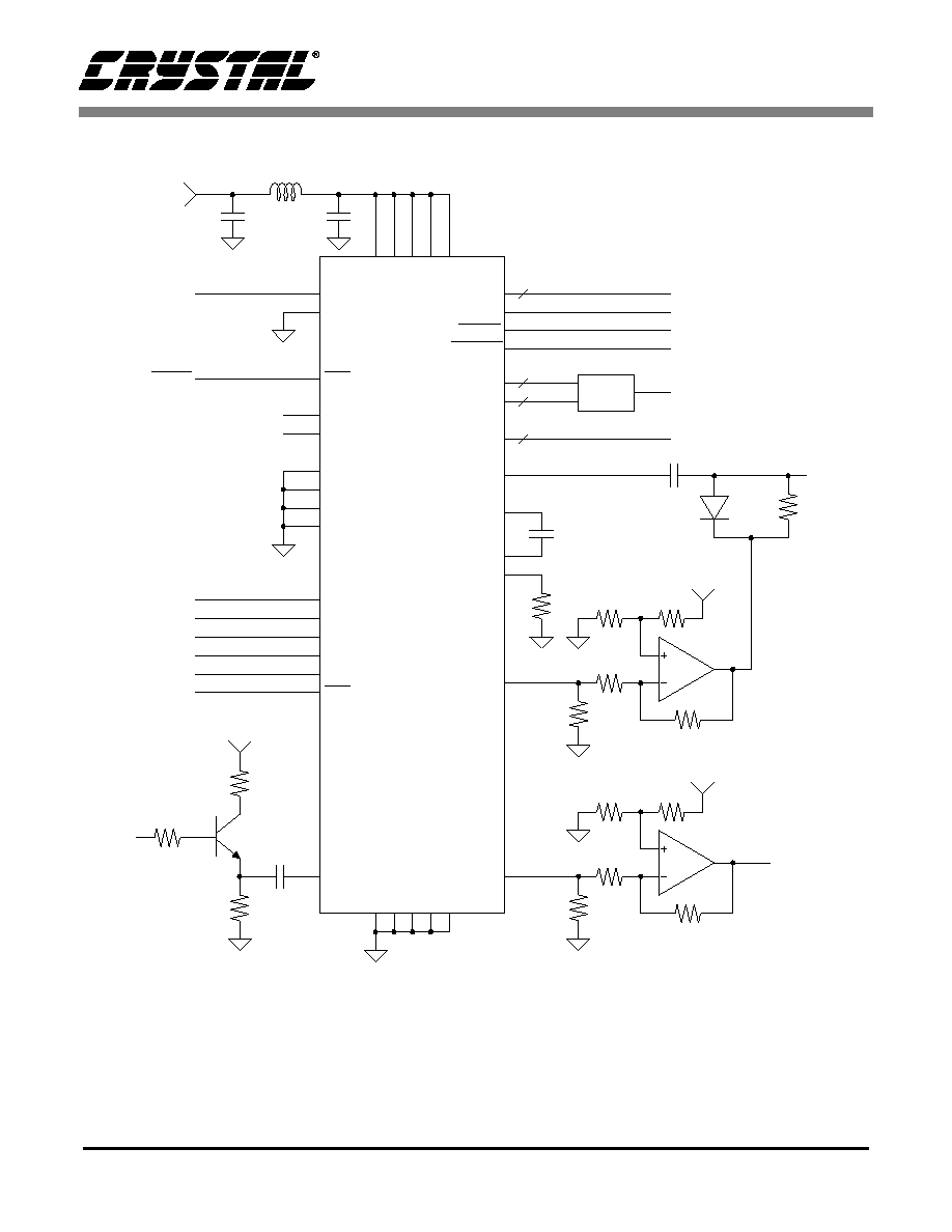
5 11 25 32 40
43
39
38
29
30
17
16
3
2
13
DOUT[0:12]
CLKO
HSYNC
RD_OUT
V[1:4]
S[1:4]
H[1:4]
RG
REF_CAPP
REF_CAPN
4
4
4
52
12
13
37
28
27
21
15
14
6
7
8
9
23
4 10 24 31 41
19
18
POWER_DOWN
EXPOSE
SCLK
SDATI
SDATO
SEN
AIN
BG_RES
DAC_OUT1
DAC_OUT2
GND
CS7620
Figure 23. Typical Connection Diagram Using Vertical and Horizontal Timing Mode

CS7620
24
DS301PP2
60.4 k
10 k
464
60.4 k
10 k
464
Substrate
Voltage
to CCD
to CCD
10 k
±1%
1 µF
to Microcontroller
to CCD
1000 pF
100 k
VCC
VAA
CLK_IN
RESET
from
Microcontroller
from
CCD
NC
NC
XTAL_IN
BYPASS_PLL
RST
DIAG0
DIAG1
SCAN_MODE
TEST
LINE_ENA
CLAMP
5
11 25 32 40
43
39
38
29
30
17
16
3
2
13
DOUT[0:12]
CLKO
HSYNC
RD_OUT
V[1:4]
S[1:4]
H[1:4]
RG
REF_CAPP
REF_CAPN
4
4
4
52
12
13
37
28
27
21
15
14
6
7
8
9
23
4
10 24 31 41
19
18
POWER_DOWN
EXPOSE
SCLK
SDATI
SDATO
SEN
AIN
BG_RES
DAC_OUT1
DAC_OUT2
GND
CS7620
NC
NC
NC
Figure 24. Typical Connection Diagram Using Horizontal Only Timing Mode

CS7620
DS301PP2
25
60.4 k
10 k
464
60.4 k
10 k
464
Substrate
Voltage
to CCD
10 k
±1%
1 µF
to Microcontroller
VCC
VAA
RESET
from
Microcontroller
from
CCD
NC
NC
XTAL_IN
BYPASS_PLL
RST
DIAG0
DIAG1
SCAN_MODE
TEST
LINE_ENA
CLAMP
5 11 25 32 40
43
39
38
29
30
17
16
3
2
13
DOUT[0:12]
CLKO
HSYNC
RD_OUT
V[1:4]
S[1:4]
H[1:4]
RG
REF_CAPP
REF_CAPN
4
4
4
52
12
13
37
28
27
21
15
14
6
7
8
9
23
4 10 24 31 41
19
18
POWER_DOWN
EXPOSE
SCLK
SDATI
SDATO
SEN
AIN
BG_RES
DAC_OUT1
DAC_OUT2
GND
CS7620
NC
NC
NC
Sampling
Signals
VDD
NC
NC
to RG bias
circuitry
CK_FT
CK_DT
Figure 25. Typical Connection Diagram Using Slave Mode

CS7620
26
DS301PP2
4
REGISTER DESCRIPTIONS
Register (hex)
Register Function
Access
Default value (hex)
00h
Software Reset
W
00
01h
Power Down Control 1
R/W
00h
02h
Power Down Control 2
R/W
00
03h-05h
Reserved
06h
Operation Control 1
R/W
09h
07h
Operation Control 2
R/W
04h
08h-0Ch
Reserved
0Dh
Black Level Control - Accumulator (LSB)
R/W
00h
0Eh
Black Level Control - Accumulator (MSB)
R/W
01h
0Fh
Black Level Control - Loop Gain, Clamp Length
R/W
0Ah
10h
Gain Calibration - Offset 1
R/W
00h
11h
Gain Calibration - Offset 2
R/W
00h
12h
Gain Calibration - Offset 3
R/W
00h
13h-15h
Reserved
16h
Gain Calibration - Fixed Gains
R/W
00h
17h
Timing Control - Number of Lines (MSB's)
R/W
05h
18h
Timing Control - Number of Lines (LSB's)
R/W
1Ch
19h
Timing Control - Number of Columns (MSB's)
R/W
06h
1Ah
Timing Control - Number of Columns (LSB's)
R/W
93h
1Bh
Timing Control - Number of Dark Rows
R/W
A4h
1Ch
Timing Control - Start of Black Pixels
R/W
04h
1Dh
Timing Control - End of Black Pixels
R/W
3Fh
1Eh
Timing Control - Number of Rows Until Active
R/W
C6h
1Fh
Timing Control - Start of Active Pixels
R/W
4Bh
20h
Timing Control - Vertical Time Division
R/W
01h
21h
Timing Control - Lines in Storage Buffer (MSB)
R/W
01h
22h
Timing Control - Lines in Storage Buffer (LSB's)
R/W
06h
23h
Timing Control - Extra Lines of Exposure in Low Resolution
Mode (MSB's)
R/W
00h
24h
Timing Control - Extra Lines of Exposure in Low Resolution
Mode (LSB's)
R/W
00h
25h
Timing Control - Vsync Mode, Low Res Sensitivity, Lines of
Exposure in Low Res Mode (MSB)
R/W
01h
26h
Timing Control - Lines of Exposure in Low Res Mode (LSB) R/W
06h
27h
Reserved
28h
Timing Control - Polarity of vertical shift outputs
R/W
FFh
29h
Horizontal Timing Control - H1
R/W
68h
2Ah
Horizontal Timing Control - H2
R/W
7Ah
2Bh
Horizontal Timing Control - H3
R/W
4Ch
2Ch
Horizontal Timing Control - H4
R/W
1Eh
2Dh
Horizontal Timing Control - Analog Delays
R/W
00h
2Eh
Compander - Black slope, Slopes (MSBs)
R/W
00h
2Fh
Compander - Slope1 (LSBs)
R/W
A8h
30h
Compande - Slope2 (LSBs)
R/W
60h
31h
Compander - Slope3 (LSBs)
R/W
20h
Table 7. Register Description

CS7620
DS301PP2
27
32h
Compander - Slope4 (LSBs)
R/W
07h
33h
Compander - Offset1
R/W
08h
34h
Compander - Offsets (MSBs)
R/W
0Bh
35h
Compander - Offset2 (LSBs)
R/W
BFh
36h
Compander - Offset3 (LSBs)
R/W
05h
37h
Compander - Offset4 (LSBs)
R/W
20h
38h
Compander - X1 (MSBs)
R/W
03h
39h
Compander - X1 (LSBs)
R/W
20h
3Ah
Compander - X2 (MSBs)
R/W
05h
3Bh
Compander - X2 (LSBs)
R/W
18h
3Ch
Compander - X3 (MSBs)
R/W
0Bh
3Dh
Compander - X3 (LSBs)
R/W
58h
3Eh
Power_up Counter
R/W
7Dh
3Fh
Valid_data/Dout edge/Clock_in divider
R/W
01h
40h
DAC #1 Control
R/W
00h
41h
DAC #2 Control
R/W
00h
42h-7Dh
Reserved
7Eh
Device ID
R
ECh
7Fh
Rev Code
R
02h
Register (hex)
Register Function
Access
Default value (hex)
Table 7. Register Description (Continued)

CS7620
28
DS301PP2
4.1
Reset
Default = 00; Write (address 00h)
4.2
Power Down Control 1
Default = 00h; Read/Write (address 01h)
Bit Number
7
6
5
4
3
2
1
0
Bit Name
Reserved
sft_rst
Default
-
-
-
-
-
-
-
00
Bit
Mnemonic
Function
7:1
-
Reserved
0
sft_rst
Software Reset: When this bit is written with a `1', all of the digital circuitry
and the registers will reset to their default values. It automatically clears after
4 pixel clock periods. The clocks remain running during the reset period.
Bit Number
7
6
5
4
3
2
1
0
Bit Name
pd_vga
pd_adc
pd_ref
Reserved
pd_dac1
pd_dac2
Reserved
Default
0
0
0
-
-
0
0
-
Bit
Mnemonic
Function
7
pd_vga
DRX Front End Power Down: When written with a `1', the DRX front end
circuitry powers down. Used for test purposes only.
6
pd_adc
ADC Power Down: When written with a `1', the Analog-to-Digital converter
circuitry powers down. Used for test purposes only.
5
pd_ref
Voltage Reference Power Down: When written with a `1', the voltage refer-
ence generator powers down. Used for test purposes only.
4:3
-
Reserved
2
pd_dac1
DAC #1 Power Down: When written with a `1', DAC #1 powers down. Should
be powered down when DAC#1 is not being used by the system.
1
pd_dac2
DAC #2 Power Down: When written with a `1', DAC #2 powers down. Should
be powered down when DAC#2 is not being used by the system.
0
-
Reserved

CS7620
DS301PP2
29
4.3
Power Down Control 2
Default = 00; Read/Write (address 02h)
4.4
Operation Control 1
Default = 09h; Read/Write (address 06h).
Bit Number
7
6
5
4
3
2
1
0
Bit Name
Reserved
pd_htim
Reserved
Default
-
-
-
-
-
-
0
-
Bit
Mnemonic
Function
7:2
-
Reserved
1
pd_htim
Horizontal Timing Power Down: When written with a `1', the horizontal tim-
ing generator powers down. Should be powered down when horizontal timing
is not being used by the system. In this mode the chip is a "timing slave."
0
-
Reserved
Bit Number
7
6
5
4
3
2
1
0
Bit Name
low_res
tim_modes2
tim_modes1
tim_modes0
bits_out1
bits_out1
blk_dis
off_range
Default
0
0
0
0
1
0
0
1
Bit
Mnemonic
Function
7
low_res
Low Resolution Mode: This mode can be used to cut the current consump-
tion of the chip by 20 mA. The output of the ADC will have 6 bits of resolution
in this mode, and the output of the chip will have 9 bits after using the DRX
circuitry. It is intended to be used when driving an LCD display or any other
time when a lower resolution picture is acceptable.
6
tim_modes2
Timing Generator Select: The type of timing signals output by the chip can
be selected using these control bits. IBM35CCDPIX13 2x2 and
IBM35CCDPIX13 3x4 modes, support type IBM CCDs with different color filter
patterns. Note that register 1Bh needs to be rewritten with correct low resolu-
tion values for black rows if low resolution mode is used (see Table 3).
The chip's default power up setting is hardcoded to be IBM35CCD2PIX1. So
that the registers that hold the number of lines, the number of pixels per line,
the number of black lines, and the number of active lines are all set up to their
proper values. If IBM35CCDPIX13 is to be used, the values on all those reg-
isters has to be changed appropriately (see Tables 5 and 6).
5
tim_modes1
4
tim_modes0
CS7620
30
DS301PP2
3
bits_out1
Number of Data Bits Out: The range of the output data can be determined
by these bits. The data internal to the chip has a 13-bit range. The output can
be this full range, half this range (12 bits), or an eighth of this range (10 bits).
If 12-bit data is selected, the top half of the 13-bit range is saturated to the
maximum 12-bit code. If 10-bit data is selected, the compander curve which
is user programmable is employed to map the 13-bit data to the 10-bit output.
0 - 10 bits output
1 - 10 bits output
2 - 13 bits output
3 - 12 bits output
2
bits_out1
1
blk_dis
Black Level Loop Disabled: If the user chooses to adjust the black level him-
self through register access, he may disable the internal black level loop. This
loop usually updates the black level to what it calculates to be the correct level.
If disabled, the offset used will be determined from the value written in the
black level accumulator register.
0 - internal black level loop is enabled
1 - black level loop is disabled
0
off_range
Offset Range: The black level loop is used to cancel any offsets from the
CCD and chip circuitry. If the offsets are small, the user has the option to de-
crease the offset cancellation range for the added advantage of increasing the
resolution of the offset cancellation.
0 - smaller offset cancellation range used (~50 mV)
1 - larger offset cancellation range used (~100 mV)
Mode value
Mode
000
IBM35CCD2PIX1 and IBM35CCDPIX13 CCD high resolution mode
001
IBM35CCD2PIX1 CCD low resolution (viewfinder) mode
010
reserved
100
reserved
101
IBM35CCD13PIX CCD (2x2) low resolution (viewfinder) mode
110
IBM35CCD13PIX CCD (3x4) low resolution (viewfinder) mode
111
external timing used
Table 8. Different Resolution Operating Modes
Bit
Mnemonic
Function

CS7620
DS301PP2
31
4.5
Operation Control 2
Default = 04h; Read/Write (address 07h).
Bit Number
7
6
5
4
3
2
1
0
Bit Name
pol_hsyncb
pol_rd_outb
dac2_mode
dac1_mode
fs_lvl1
fs_lvl0
gain_cal1
gain_cal2
Default
0
0
0
0
0
1
0
0
Bit
Mnemonic
Function
7
pol_hsyncb
Hsync Polarity: The HSYNC signal output from the chip defaults to be high
when data is being shifted out of the CCD and low during all other times (the
vertical shift time of each line and idle times). This polarity may be swapped
with this bit so that HSYNC is low when data is being shifted out and high all
other times.
0 - HSYNC is high during horizontal data read out
1 - HSYNC is low during horizontal data read out
6
pol_rd_outb
Rd_Out Polarity: The RD_OUT signal output from the chip defaults to be low
when the CCD data readout is being performed and high when not reading out
data from the CCD. The polarity of this signal may be swapped with this bit so
that RD_OUT is high during readout and low when not reading data out. Note
that when this bit is redefined in order to function as a vertical sync signal, this
bit will serve to swap its polarity as well.
5
dac2_mode
Dac #2 Current Mode: There are two modes for the output current of DAC2.
Default mode provides a current range of 2.2 mA for the 8-bit input word. This
will increment the current by ~8.6 µA per LSB code change. The high current
mode can be selected using this bit to change the current range to 8.7 mA for
the 8-bit input word. This will increment the current by ~34 µA per LSB code
change.
4
dac1_mode
Dac #1 Current Mode: There are two modes for the output current of DAC1.
Default mode provides a current range of 2.2 mA for the 8-bit input word. This
will increment the current by ~8.6 µA per LSB code change. The high current
mode can be selected using this bit to change the current range to 8.7 mA for
the 8-bit input word. This will increment the current by ~34 µA per LSB code
change.
3
fs_lvl1
Full Scale Level: This is used to set the full scale input range of the CS7620.
Since CCDs have various saturation levels, it is advantageous to set the full
scale input range of the CS7620 to match the saturation level of the CCD
used. Table 9 shows the full scale level choices
2
fs_lvl0
1
gain_cal1
Gain Calibration #1: A calibration of the gain stages is required to insure a
monotonic digital output. In default (`0'), this calibration is automatically done
after a chip reset and after coming up from power down mode. If the recalibra-
tion after power down is not desired, this bit can be written with a `1' to force
a calibration only after a chip reset.
0
gain_cal2
Gain Calibration #2: A calibration of the gain stages is required to insure a
monotonic digital output. This calibration is transparent to the user. However,
if the user wishes to force a calibration to occur, he may do so by setting this
bit to `1', which will invoke a gain calibration sequence immediately. This bit
automatically clears itself after a calibration has been initiated.
CS7620
32
DS301PP2
4.6
Black Level Control - Accumulator (LSB)
Default = 00h; Read/Write (address 0Dh)
4.7
Black Level Control - Accumulator (MSB)
Default = 01h; Read/Write (address 0Eh).
fs_lvl
Full Scale Voltage
00
0.53 V
01
1.07 V
1X
1.60 V
Table 9. Full Scale Level Choices
Bit Number
7
6
5
4
3
2
1
0
Bit Name
accumulator7 accumulator6 accumulator5 accumulator4 accumulator3 accumulator2 accumulator1 accumulator0
Default
0
0
0
0
0
0
0
0
Bit
Mnemonic
Function
7
accumulator7
Black Level Accumulator: See Description of register 0Eh.
6
accumulator6
5
accumulator5
4
accumulator4
3
accumulator3
2
accumulator2
1
accumulator1
0
accumulator0
Bit Number
7
6
5
4
3
2
1
0
Bit Name
Reserved
accumulator8
Default
-
-
-
-
-
-
-
1
Bit
Mnemonic
Function
7:1
-
Reserved
0
accumulator8
Black Level Accumulator: The black level accumulator is a 9 bit number rep-
resenting an amount of offset added to the input of the CDS circuit. The black
level loop alters the black level accumulator value to make the output of the
ADC settle to code 64 during black pixels. If desired the black loop may be
disabled and written to manually to add any desired amount of offset. There
is a total of ~100 mV of offset range if the offset range register setting is set to
1 or ~50 mV when this register setting is set to "0". This offset range is used
to correct for CCD offsets plus internal offsets generated in the analog path of
this chip. The offset range before subtracting the internal offsets is as shown
in Table 10 below with the worst case internal offsets being ±17 mV.
Offset Range (Reg
06h bit 0)
Max Offset Blk Acc=511
Min Offset Blk Acc=0
Accumulator LSB Size
1
~30 mV
~-72 mV
~0.2 mV
0
~11 mV
~-40 mV
~0.1 mV
Table 10. Offset Range
CS7620
DS301PP2
33
4.8
General Black Level
The black loop is a feedback system that causes the ADC output to settle to 64 during the register defined black
pixels. This has the purpose of removing any CCD and system offsets and defining 64 as the known black level.
The loop has an exponential settling response and the time constant of this loop is effected by the black loop gain
and the number of black pixels to accumulate before updating the black accumulator. See Figure 10 for a block
diagram of the black level.
4.9
Black Level Control - Loop Gain, Clamp Length
Default = 0Ah; Read/Write (address 0Fh).
Where:
K = 1/256*blk_gain
n = Black loop clamp length = blk_clp_l[5:0]
fu = update rate
Bit Number
7
6
5
4
3
2
1
0
Bit Name
blk_gain1
blk_gain0
blk_clp_15
blk_clp_14
blk_clp_13
blk_clp_12
blk_clp_11
blk_clp_10
Default
0
0
0
0
1
0
1
0
Bit
Mnemonic
Function
7
blk_gain1
Black Loop Gain Factor: The Black loop gain factor can be set to 1x,2x,4x,or
8x and is simply a multiplying constant to effect the weight of each black pixel
before it is accumulated.
00 - defines a gain of 1x
01 - defines a gain of 2x
10 - defines a gain of 4x
11 - defines a gain of 8x
6
blk_gain0
5
blk_clp_15
Black Loop Clamp Length: The black clamp length effects the loop time con-
stant and also acts to average out noise in the black level. The larger this val-
ue the more pixels that are summed before the loop is updated which causes
greater averaging and a smaller settling time constant.
Table 11 shows the black loop time constant for various settings of Offset
Range (register 06h, bit 0) and Fixed Gain Settings (register 16h, bits 5-3).
4
blk_clp_14
3
blk_clp_13
2
blk_clp_12
1
blk_clp_11
0
blk_clp_10
Fixed Gain
(Register 16h)
Offset Range = 1
Offset Range = 0
not fixed
-1/(ln(1-nK))(1/fu)
-1/(ln(1-nK/2))(1/fu)
x1
-1/(ln(1-nK/8))(1/fu)
-1/(ln(1-nK/16))(1/fu)
x2
-1/(ln(1-nK/4))(1/fu)
-1/(ln(1-nK/8))(1/fu)
x4
-1/(ln(1-nK/2))(1/fu)
-1/(ln(1-nK/4))(1/fu)
x8
-1/(ln(1-nK))(1/fu)
-1/(ln(1-nK/2))(1/fu)
Table 11. Black Loop Time Constant

CS7620
34
DS301PP2
4.10
Gain Calibration - Offset 1
Default = 00h; Read/Write (address 10h)
4.11
Gain Calibration - Offset 2
Default = 00h; Read/Write (address 11h)
Bit Number
7
6
5
4
3
2
1
0
Bit Name
gain_offset17
gain_offset16
gain_offset15
gain_offset14
gain_offset13 gain_offset 12 gain_offset11
gain_offset10
Default
0
0
0
0
0
0
0
0
Bit
Mnemonic
Function
7
gain_offset17
Gain Calibration Offset 1: Offset added to 4x gain segment, values are in 2's
complement. See details in register 12h.
6
gain_offset16
5
gain_offset15
4
gain_offset14
3
gain_offset13
2
gain_offset12
1
gain_offset11
0
gain_offset10
Bit Number
7
6
5
4
3
2
1
0
Bit Name
gain_offset27 gain_offset26 gain_offset25 gain_offset24 gain_offset23
gain_offset
22
gain_offset21 gain_offset20
Default
0
0
0
0
0
0
0
0
Bit
Mnemonic
Function
7
gain_offset27
Gain Calibration Offset 2: Offset added to 2x gain segment, values are in 2's
complement. See details in register 12h.
6
gain_offset26
5
gain_offset25
4
gain_offset24
3
gain_offset23
2
gain_offset22
1
gain_offset21
0
gain_offset20

CS7620
DS301PP2
35
4.12
Gain Calibration - Offset 3
Default = 00h; Read/Write (address 11h)
Gain Calibration - Fix Gains
Default = 00h; Read/Write (address 16h)
Bit Number
7
6
5
4
3
2
1
0
Bit Name
gain_offset
37
gain_offset
36
gain_offset
35
gain_offset
34
gain_offset
33
gain_offset
32
gain_offset
31
gain_offset
30
Default
0
0
0
0
0
0
0
0
Bit
Mnemonic
Function
7
gain_offset37
Gain Calibration Offset 3: Offset added to 1x gain segment. Values are in
2's complement.
These registers are used to report some of the calibration settings. After cal-
ibration is performed the gain offset registers are automatically updated with
values needed for the DRX circuitry to operate correctly. These registers
should not be written to since this will remove the proper settings found during
calibration. The gain offset values are used to add an offset to the output of
the ADC when using different analog gain settings (See equations below).
The purpose of this is to produce a continuous transition between the different
gain settings so that the final 13 bit output is monotonic and has no undesired
artifacts. (See Figure 26)
{ADC_outif in the 8x gain segment}
dout[12:0] ={ADC_out*2+Offset1if in the 4x gain segment}
{ADC_out*4+Offset2*2if in the 2x gain segment}
{ADC_out*8+Offset3*4if in the 1x gain segment}
6
gain_offset36
5
gain_offset35
4
gain_offset34
3
gain_offset33
2
gain_offset32
1
gain_offset31
0
gain_offset30
Bit Number
7
6
5
4
3
2
1
0
Bit Name
Reserved
fixed_gain2
fixed_gain1
fixed_gain0
Reserved
Default
-
-
0
0
0
-
-
-
Bit
Mnemonic
Function
7:6
-
Reserved
5
fixed_gain2
Fixed Gain: This is used to turn off the DRX functionality and apply a fixed
gain to the input before reaching the ADC. A setting of 000 is used for normal
operation this will yield the largest dynamic range by switching the front end
gain relative to the amplitude of the input signal. The settings 001, 010, 011,
and 100 are for fixed gains of 1x, 2x, 4x, and 8x respectively. Figure 27 shows
the transfer function of the output of the ADC for a given input with the various
fixed gain settings.
4
fixed_gain1
3
fixed_gain0
2:0
-
Reserved
CS7620
36
DS301PP2
4.13
Timing Control - Number of Lines (MSBs)
Default = 05h; Read/Write (address 17h)
Bit Number
7
6
5
4
3
2
1
0
Bit Name
Reserved
num_lines12
num_lines11
num_lines10
num_lines9 num_lines8
Default
-
-
-
0
0
1
0
1
Bit
Mnemonic
Function
7:5
-
Reserved
4
num_lines12
Line Numbers: Bits 12 through 8 of the number of lines. (See Figure 26)
3
num_lines11
2
num_lines10
1
num_lines9
0
num_lines8
1024
512
1X
2X
4X
8X
ADC OUT
INPUT
1.07
8192
4096
1024
2048
64
Figure 26. Transfer Function of Analog Input to Digital Output (assuming full scale level of 1.07V)
64
INPUT
USE OFF
SET1
USE OFFSET
2
USE OFFSET
3

CS7620
DS301PP2
37
1024
1X
2X
4X
8X
ADC OUTPUT
1024
Figure 27. Transfer Function of ADC with Fixed Gain Settings (assuming full scale level of 1.07V)
INPUT
0.13
0.27
0.53
1.07
ADC OUTPUT
1X
INPUT (V)
1.07
1024
ADC OUTPUT
2X
INPUT (V)
1.07
0.53
1024
ADC OUTPUT
4X
INPUT (V)
1.07
1024
ADC OUTPUT
8X
INPUT (V)
1.07
0.53
0.27
0.53
0.13
0.27
FIXED GAIN = 001
FIXED GAIN = 000
FIXED GAIN = 011
FIXED GAIN = 100
FIXED GAIN = 010

CS7620
38
DS301PP2
4.14
Timing Control - Number of Lines (LSBs)
Default = 1Ch; Read/Write (address 18h)
4.15
Timing Control - Number of Columns (MSBs)
Default = 06h; Read/Write (address 19h)
Bit Number
7
6
5
4
3
2
1
0
Bit Name
num_lines7 num_lines6 num_lines5 num_lines4 num_lines3 num_lines2 num_lines1 num_lines0
Default
0
0
0
1
1
1
0
0
Bit
Mnemonic
Function
7
num_lines7
Line Numbers: Bits 7 through 0 of the number of lines.
The number of lines registers should be written with the total number of lines
(rows) of the CCD including any black lines (this should not include the trans-
fer area).
The default value is 1308 which is the number of lines in a IBM35CCD2PIX1
CCD. (See Figure 28)
6
num_lines6
5
num_lines5
4
num_lines4
3
num_lines3
2
num_lines2
1
num_lines1
0
num_lines0
Bit Number
7
6
5
4
3
2
1
0
Bit Name
Reserved
num_pixels12 num_pixels11 num_pixels10
num_pixels9
num_pixels8
Default
-
-
-
0
0
1
1
0
Bit
Mnemonic
Function
7:5
-
Reserved
4
num_pixles12
Column Numbers: Bits 12 through 8 of the number of columns. (See
Figure 28)
3
num_pixels11
2
num_pixels10
1
num_pixels9
0
num_pixels8
CS7620
DS301PP2
39
4.16
Timing Control - Number of Columns (LSBs)
Default = 93h; Read/Write (address 1Ah)
4.17
Timing Control - Number of Dark Rows
Default = A4h; Read/Write (address 1Bh)
Bit Number
7
6
5
4
3
2
1
0
Bit Name
num_pixels7
num_pixels6
num_pixels5
num_pixels4
num_pixels3
num_pixels2
num_pixels1
num_pixels0
Default
1
0
0
1
0
0
1
1
Bit
Mnemonic
Function
7
num_pixels7
Column Numbers: Bits 7 through 0 of the number of columns.
The number of columns registers should be written with the total number of
pixels per line (columns) of the CCD including any black pixels and any extra
pixels. (due to CCD horizontal register latency)
The default value (num_pixels[12:0]) is 1683 which is the number of rows in a
IBM35CCD2PIX1 CCD. (See Figure 28)
6
num_pixels6
5
num_pixels5
4
num_pixels4
3
num_pixels3
2
num_pixels2
1
num_pixels1
0
num_pixels0
Bit Number
7
6
5
4
3
2
1
0
Bit Name
drk_rws_frst3 drk_rws_frst2 drk_rws_frst1 drk_rws_frst0
drk_rws_lst3
drk_rws_lst2
drk_rws_lst1
drk_rws_lst0
Default
1
0
1
0
0
1
0
0
Bit
Mnemonic
Function
7
drk_rws_frst3
Dark Rows: The dark rows registers should be written with the number of
rows at the top and bottom of the CCD.
Please note that drk_rws_frst refers to the first rows to be read out. These are
the rows at the top of the image, which get inverted through the lens, and get
focused onto the bottom rows of the CCD.
The CS7620 uses these rows to acquire the proper black level.
The default value is 10 and the correct value to work with the
IBM35CCD2PIX1 CCD. (See Figure 28)
6
drk_rws_frst2
5
drk_rws_frst1
4
drk_rws_frst0
3
drk_rws_lst3
Dark Rows: The dark rows registers should be written with the number of
rows at the top and bottom of the CCD.
Note that drk_rws_lst refers to the last rows to be read out. This are the rows
at the bottom of the image, which get inverted through the lens, and get fo-
cused onto the top rows of the CCD.
The CS7620 uses these rows to acquire the proper black level.
The default value is 4 and is the correct value to work with the
IBM35CCD2PIX1 CCD. (See Figure 28)
2
drk_rws_lst2
1
drk_rws_lst1
0
drk_rws_lst0

CS7620
40
DS301PP2
4.18
Timing Control - Start of Black Pixels
Default = 04h; Read/Write (address 1Ch)
4.19
Timing Control - End of Black Pixels
Default = 3Fh; Read/Write (address 1Dh)
Bit Number
7
6
5
4
3
2
1
0
Bit Name
Reserved
blk_begin3
blk_begin2
blk_begin1
blk_begin0
Default
-
-
-
-
0
1
0
0
Bit
Mnemonic
Function
7:4
-
Reserved
3
blk_begin3
Black Pixels: This register indicates the beginning of the black pixels within
a horizontal line.
Before the black pixels, there can be some extra pixels, due to latency through
the horizontal shift register inside the CCD. The default value for this register
is 4, since IBM35CCD2PIX1 has 3 extra pixels. (See Figure 28)
2
blk_begin2
1
blk_begin1
0
blk_begin0
Bit Number
7
6
5
4
3
2
1
0
Bit Name
Reserved
blk_end6
blk_end5
blk_end4
blk_end3
blk_end2
blk_end1
blk_end0
Default
-
0
1
1
1
1
1
1
Bit
Mnemonic
Function
7
-
Reserved
6
blk_end6
Black Pixels: This register indicates the end of the black pixels within the hor-
izontal line.
This register is used by the black level loop together with blk_begin, to acquire
the proper black level on a line by line basis. Since the loop has some latency,
the value stored in this register, should be 10 less than the actual last black
pixel in each line. Since in IBM35CCD2PIX1, this number is 73, the default is
set to 63. (See Figure 28)
5
blk_end5
4
blk_end4
3
blk_end3
2
blk_end2
1
blk_end1
0
blk_end0
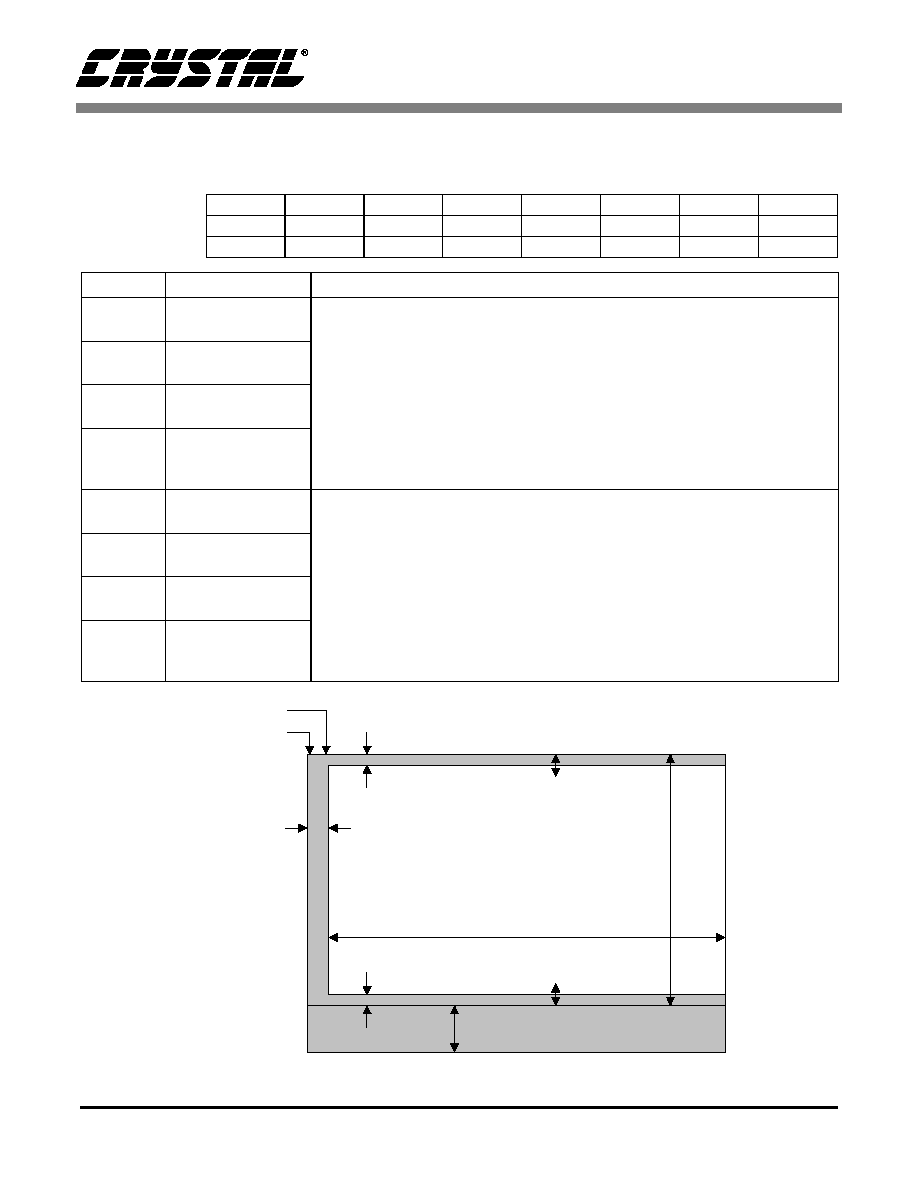
CS7620
DS301PP2
41
4.20
Timing Control - Number of Rows until Active
Default = C6h; Read/Write (address 1Eh)
Bit Number
7
6
5
4
3
2
1
0
Bit Name
act_rws_frst3 act_rws_frst2 act_rws_frst1 act_rws_frst0 act_rws_lst3
act_rws_lst2
act_rws_lst1
act_rws_lst0
Default
1
1
0
0
0
1
1
0
Bit
Mnemonic
Function
7
act_rws_frst3
Active Rows: act_rws_frst corresponds to the first group of non active rows
at the top of the image, which get inverted through the lens, and get focused
onto the bottom rows of the CCD.
The register value is used by the CS7620 when the part is in the valid data
mode to generate the data valid signal on the CLKO pin.
Valid data can be set through the above mentioned registers together with
act_begin(1Fh) to define a subset of pixels to be passed to the subsequent
ASIC or DSP component. This subset may or may not include dark rows
and/or dark pixels. Please refer to Figure 28.
6
act_rws_frst2
5
act_rws_frst1
4
act_rws_frst0
3
act_rws_lst3
Active Rows: act_rws_lst corresponds to the last group of non active rows at
the bottom of the image, which get inverted through the lens, and get focused
onto the top rows of the CCD.
The register value is used by the CS7620 when the part is in the valid data
mode to generate the data valid signal on the CLKO pin.
Valid data can be set through the above mentioned registers together with
act_begin(1Fh) to define a subset of pixels to be passed to the subsequent
ASIC or DSP component. This subset may or may not include dark rows
and/or dark pixels. Please refer to Figure 28.
2
act_rws_lst2
1
act_rws_lst1
0
act_rws_lst0
Da
r
k
P
i
x
e
ls
drk_rws_lst (1Bh)
blk_begin (1Ch)
blk_end (1Dh)
Dark Pixels
act_rws_lst (1Eh)
num_pixels (19h, 1Ah)
num_lines (17h, 18h)
act_rws_frst (1Eh)
shiftl_num (21h, 22h)
drk_rws_frst (1Bh)
ACTIVE PIXELS
TRANSFER
AREA
Figure 28. Typical CCD Pixel Arrangement

CS7620
42
DS301PP2
4.21
Timing Control - Start of Active Pixels
Default = 4Bh; Read/Write (address 1Fh)
4.22
Timing Control - Vertical Time Division
Default = 01h; Read/Write (address 20h)
Bit Number
7
6
5
4
3
2
1
0
Bit Name
act_begin7
act_begin6
act_begin5
act_begin4
act_begin3
act_begin2
act_begin1
act_begin0
Default
0
1
0
0
1
0
1
1
Bit
Mnemonic
Function
7
act_begin7
Active Pixels: This register should be programmed with the pixel number of
the first active pixel to be read out. That is the first pixel after the extra pixels,
the black pixels, and the grey pixel.
This register value is used by the CS7620 when the part is in the valid data
mode to generate the data valid signal on the CLKO pin.
Valid data can be set through the above mentioned registers together with
act_begin(1Fh) to define a subset of pixels to be passed to the subsequent
ASIC or DSP component. This subset may or may not include dark rows
and/or dark pixels. Please refer to Figure 28.
The default value is set to 75, which is the sum of the blk_end register (1Dh)
and act_rws_lst register (1Eh).
6
act_begin6
5
act_begin5
4
act_begin4
3
act_begin3
2
act_begin2
1
act_begin1
0
act_begin0
Bit Number
7
6
5
4
3
2
1
0
Bit Name
Reserved
tdv4
tdv3
tdv2
tdv1
tdv0
Default
-
-
-
0
0
0
0
1
Bit
Mnemonic
Function
7:5
-
Reserved
4
tdv4
Critical Timing: This determines the width of the minimum vertical division
measured in pixel clocks. (One vertical pixel shift (row) requires 8 vertical time
division slots) See Figure 33.
3
tdv3
2
tdv2
1
tdv1
0
tdv0

CS7620
DS301PP2
43
4.23
Timing Control - Lines in Storage Buffer (MSBs)
Default = 01h; Read/Write (address 21h)
4.24
Timing Control - Lines in Storage Buffer (LSBs)
Default = 06h; Read/Write (address 22h)
4.25
Timing Control - Extra Lines of Exposure in Low Resolution Mode (MSBs)
Default = 00h; Read/Write (address 23h)
Bit Number
7
6
5
4
3
2
1
0
Bit Name
Reserved
shiftl_num9 shiftl_num8
Default
-
-
-
-
-
-
0
1
Bit
Mnemonic
Function
7:2
-
Reserved
1
shiftl_num9
Storage Buffer Lines: This value must be programmed for proper operation
in both high and low resolution modes.
Please refer to Figure 28.
0
shiftl_num8
Bit Number
7
6
5
4
3
2
1
0
Bit Name
shiftl_num7 shiftl_num6 shiftl_num5 shiftl_num4 shiftl_num3 shiftl_num2 shiftl_num1 shiftl_num0
Default
0
0
0
0
0
1
1
0
Bit
Mnemonic
Function
7
shiftl_num7
Storage Buffer Lines: This value must be programmed for proper operation
in both high and low resolution modes.
The default value for shiftl_num is 262.
Please refer to Figure 28.
6
shiftl_num6
5
shiftl_num5
4
shiftl_num4
3
shiftl_num3
2
shiftl_num2
1
shiftl_num1
0
shiftl_num0
Bit Number
7
6
5
4
3
2
1
0
Bit Name
Reserved
n_extra10
n_extra9
n_extra8
Default
-
-
-
-
-
0
0
0
Bit
Mnemonic
Function
7:3
-
Reserved
2
n_extra10
Extra Lines: See description for register 24h below.
1
n_extra9
0
n_extra8
CS7620
44
DS301PP2
4.26
Timing Control - Extra Lines of Exposure in Low Resolution Mode (LSBs)
Default = 00h; Read/Write (address 24h)
4.27
Timing Control - Vsync Mode, Lines of Exposure in Low Resolution Mode (MSBs)
Default = 01h; Read/Write (address 25h)
Bit Number
7
6
5
4
3
2
1
0
Bit Name
n_extra7
n_extra6
n_extra5
n_extra4
n_extra3
n_extra2
n_extra1
n_extra0
Default
0
0
0
0
0
0
0
0
Bit
Mnemonic
Function
7
n_extra7
Extra Lines: This allows for increased exposure time while in low resolution
mode.
In low resolution mode, the CS7620 continuously outputs data on a frame by
frame basis; so it can drive a LCD panel in a video mode. In this mode the
CS7620 ignores the expose signal. The default expose time is equivalent to
262 line times (see registers 25h and 26h, n_int).
N_extra provides a way to increase the exposure time beyond the one which
is set by register n_int (25h and 26h). The value of n_extra corresponds to the
number of line times.
6
n_extra6
5
n_extra5
4
n_extra4
3
n_extra3
2
n_extra2
1
n_extra1
0
n_extra0
Bit Number
7
6
5
4
3
2
1
0
Bit Name
Reserved
vsync_md
lowres_sen3
lowres_sen2
lowres_sen1
lowres_sen0
n_int8
Default
-
-
0
0
0
0
0
1
Bit Mnemonic
Function
7:6
-
Reserved
5
vsync_md
Vertical Sync: Vsync_md, will switch the RD_OUT pin to output a vertical sync signal on this
pin when the vsync_md register is set to 1. The default is 0 which outputs the RD_OUT signal
(see Figures 21 and 22).

CS7620
DS301PP2
45
4
lowres_sen3
Sensitivity in Low Resolution Mode: lowres_sens provides a way to increase the sensitivity
during low resolution mode (see Figure 33).
For proper settings of these values, please refer to the CCD data sheets.
In order to allow for a video mode, (low resolution) IBM 1.3Mpixel and 2.0Mpixel have a storage
area that is in both cases 262 lines long. The use of this transfer area, is to keep the pixels cov-
ered from light during readout. This must be done because it is not practical to have a shutter
at such high speed. Without the storage area the picture would be smeared, since the last line
to be readout would have had a lot more exposure time than the first one.
To solve this the storage area is used in the following manner. In the 1.3Mpixel there are 4 times
more active lines than there are storage lines. The low resolution mode consists of two steps:
Step 1: transfer:
During this step, the active lines are subsampled into the storage area. In the 1.3Mpixel there
are 4 times more active lines than there are storage lines, so that active line one will be stored
into storage line 1, active line 5 will be stored into storage line 2, active line 9 into storage line 3
and so on until finally active line 1045 will be stored into storage line 262.
Step 2: readout:
During this step, the data in the storage area is transferred line by line into the horizontal regis-
ter, from where it will be read out sequentially.
By using this optically covered transfer area, there is still a minimum amount of smear in the low
resolution mode. However, it is greatly reduced. This smear will only take place during the trans-
fer time, because the pixels in the active area are constantly being exposed since the shutter is
always open in the low resolution mode. This however is a small percentage of the total expo-
sure.
Sensitivity:
The sensitivity of the CCD to light can be increased by 2x or 3x in the IBM 2.0M with RGRG,
GBGB Bayer pattern. With a 2x extra sensitivity, twice as many photons will be accumulated.
This mode can be used to increase resolution in low light scenes, and should be part of the
AGC/iris control loop.
To achieve this extra sensitivity, 2 lines from the active area get added together into one line in
the storage area. this is done by having an additional pulse on the s1 line (see Figure 33).
Below are some examples:
All of this can be programmed using register lowres_sen(25h).
Each bit of this register controls one pulse.
The first pulse is always on.
0000 means only first pulse is on
1000 means the second and first pulse are on
0100 means the third and first pulse are on
0010 means the fourth and first pulse are on
0001 means the fifth and first pulse are on
0101 means the third, fifth and first pulse are on
Note that the user has to select very carefully the lines to be added. The selection of the lines is
based on the color coating of the CCD. In some cases of color coating it is possible to add 2
lines, in other cases it is possible to add 3 lines (see below).
(R = Red Pixel, B = Blue Pixel, G = Green Pixel)
3
lowres_sen2
2
lowres_sen1
1
lowres_sen0
Bit Mnemonic
Function

CS7620
46
DS301PP2
0
n_int8
Exposure Time in Low Resolution Mode: Number of lines of exposure during readout (262 =
all readout).
See register 26h for more details.
Bit Mnemonic
Function
(1) 0000
(1+3) 0100
(1+3+5) 0101
(1+5) 0001
1x
2x+
3x+
2x
RGRGR
GBGBG
RGRGR
GBGBG
RGRGR
(line 1)
(line 5)
(1) 0000
(1+4) 0010
1x
2x+
RGBRG
GBRGB
BRGBR
RGBRG
GBRGB
(line 1)
(line 5)
Figure 29. 2 million pixel IBM CCD (5:1 reduction)
Figure 30. 2 million pixel IBM CCD (5:1 reduction) RGB
pattern
* note that in this mode the RGB pattern
switches to RBG in the vertical direction.
(1) 0000
(1+4) 0010
1x
2x+
RGBR
GBRG
BRGB
RGBR
GBRG
(line 1)
(line 5)
(1) 0000
(1+3) 0100
1x
2x
RGRGRGRG
GBGBGBGB
RGRGRGRG
GBGBGBGB
RGRGRGRG
(line 1)
(line 8)
Line 1
Line 2
Line 1+
Line 2+
(6)
(6+8)
GBGBGBGB
RGRGRGRG
GBGBGBGB
Figure 31. 1.3 million pixel IBM CCD (8:2 reduction)
Figure 32. 1.3 million pixel IBM CCD (4:1 reduction)
RGB pattern
Optional
lowres_sen3
Optional
lowres_sen2
Optional
lowres_sen1
Optional
lowres_sen0
V1
V2
V3
V4
S1
S2
S3
S4
TDV (20h)
Figure 33. Vertical Timing Division for Low Resolution Mode

CS7620
DS301PP2
47
4.28
Timing Control - Lines of Exposure in Low Resolution Mode (MSBs)
Default = 06h; Read/Write (address 26h)
4.29
Timing Control - Polarity of Vertical Shift Outputs
Default = FFh; Read/Write (address 28h)
Bit Number
7
6
5
4
3
2
1
0
Bit Name
n_int7
n_int6
n_int5
n_int4
n_int3
n_int2
n_int1
n_int0
Default
0
0
0
0
0
1
1
0
Bit
Mnemonic
Function
7
n_int7
Exposure Time in Low Resolution Mode: In low resolution mode, the
CS7620 continuously outputs data on a frame by frame basis; so it can drive
a LCD panel in a video mode. In this mode the CS7620 ignores the expose
signal.
N_int allows to shorten the exposure time while in low resolution mode.
N_int controls the amount of time (measured in readout lines) where the CCD
will be exposed to light. The default is 262, this means that the CCD receives
full exposure during readout. By decreasing n_int, the amount of exposure can
be decreased. To further increase this exposure time beyond the full 262 lines
of readout time, the n_extra register (23h and 24h) is provided.
6
n_int6
5
n_int5
4
n_int4
3
n_int3
2
n_int2
1
n_int1
0
n_int0
Bit Number
7
6
5
4
3
2
1
0
Bit Name
v_polarity7
v_polarity6
v_polarity5
v_polarity4
v_polarity3
v_polarity2
v_polarity1
v_polarity0
Default
1
1
1
1
1
1
1
1
Bit
Mnemonic
Function
7
v_polarity7
Vertical Signal Polarity: Polarity of each of the eight vertical shift outputs
(V1 V2 V3 V4 S1 S2 S3 S4), where V1 polarity = MSB, S4 polarity = LSB
A "0" indicates that the signal state is low, a "1" indicates that the signal state
is high.
6
v_polarity6
5
v_polarity5
4
v_polarity4
3
v_polarity3
2
v_polarity2
1
v_polarity1
0
v_polarity0

CS7620
48
DS301PP2
4.30
Horizontal Timing Control - H1
Default = 68h; Read/Write (address 29h)
Bit Number
7
6
5
4
3
2
1
0
Bit Name
Reserved
h1d
h1f_reg2
h1f_reg1
h1f_reg0
h1f_reg2
h1f_reg1
h1f_reg0
Default
-
1
1
0
1
0
0
0
Bit
Mnemonic
Function
7
-
Reserved
6
h1d
H1 Default Setting: During the vertical shift time, the horizontal clocks are
held in one state. This bit controls whether H1 is held high or low during this
time.
A "0" indicates that the signal state is low, a "1" indicates that the signal state
is high.
5
h1f_reg2
H1 Falling Edge: The phase of the falling edge of H1 can be programmed
through this register. The falling edge of H1 corresponds to the rising edge of
the internally selected clock. The phases of these clocks are shown in Figure
19, with the complemented clocks being the inverse of these.
0 = t0
1 = t1
2 = t2
3 = t3
4 = t4
5 = t5
6 = t6
7 = t7
(See Figure 19)
4
h1f_reg1
3
h1f_reg0
2
h1f_reg2
H1 Rising Edge: The phase of the rising edge of H1 can be programmed
through this register. The rising edge of H1 corresponds to the rising edge of
the internally selected clock. The phases of these clocks are shown in Figure
19, with the complemented clocks being the inverse of these.
0 = t0
1 = t1
2 = t2
3 = t3
4 = t4
5 = t5
6 = t6
7 = t7
(See Figure 19)
1
h1f_reg1
0
h1f_reg0

CS7620
DS301PP2
49
4.31
Horizontal Timing Control - H2
Default = 7Ah; Read/Write (address 2Ah)
Bit Number
7
6
5
4
3
2
1
0
Bit Name
Reserved
h2d
h2f_reg2
h2f_reg1
h2g_reg0
h2g_reg2
h2g_reg1
h2g_reg0
Default
-
1
1
1
1
0
1
0
Bit
Mnemonic
Function
7
-
Reserved
6
h2d
H2 Default Setting: During the vertical shift time, the horizontal clocks are
held in one state. This bit controls whether H2 is held high or low during this
time.
A "0" indicates that the signal state is low, a "1" indicates that the signal state
is high.
5
h2f_reg2
H2 Falling Edge: The phase of the falling edge of H2 can be programmed
through this register. The falling edge of H2 corresponds to the rising edge of
the internally selected clock. The phases of these clocks are shown in Figure
19, with the complemented clocks being the inverse of these.
0 = t0
1 = t1
2 = t2
3 = t3
4 = t4
5 = t5
6 = t6
7 = t7
(See Figure 19)
4
h2f_reg1
3
h2g_reg0
2
h2g_reg2
H2 Rising Edge: The phase of the rising edge of H2 can be programmed
through this register. The rising edge of H2 corresponds to the rising edge of
the internally selected clock. The phases of these clocks are shown in Figure
19, with the complemented clocks being the inverse of these.
0 = t0
1 = t1
2 = t2
3 = t3
4 = t4
5 = t5
6 = t6
7 = t7
(See Figure 19)
1
h2g_reg1
0
h2g_reg0

CS7620
50
DS301PP2
4.32
Horizontal Timing Control - H3
Default = 4Ch; Read/Write (address 2Bh)
Bit Number
7
6
5
4
3
2
1
0
Bit Name
Reserved
h3d
h3f_reg2
h3f_reg1
h3f_reg0
h3f_reg2
h3f_reg1
h3f_reg0
Default
-
1
0
0
1
1
0
0
Bit
Mnemonic
Function
7
-
Reserved
6
h3d
H3 Default Setting: During the vertical shift time, the horizontal clocks are
held in one state. This bit controls whether H3 is held high or low during this
time.
A "0" indicates that the signal state is low, a "1" indicates that the signal state
is high.
5
h3f_reg2
H3 Falling Edge:The phase of the falling edge of H3 can be programmed
through this register. The falling edge of H3 corresponds to the rising edge of
the internally selected clock. The phases of these clocks are shown in Figure
19, with the complemented clocks being the inverse of these.
0 = t0
1 = t1
2 = t2
3 = t3
4 = t4
5 = t5
6 = t6
7 = t7
(See Figure 19)
4
h3f_reg1
3
h3f_reg0
2
h3f_reg2
H3 Rising Edge:The phase of the rising edge of H3 can be programmed
through this register. The rising edge of H3 corresponds to the rising edge of
the internally selected clock. The phases of these clocks are shown in Figure
19, with the complemented clocks being the inverse of these.
0 = t0
1 = t1
2 = t2
3 = t3
4 = t4
5 = t5
6 = t6
7 = t7
(See Figure 19)
1
h3f_reg1
0
h3f_reg0
CS7620
DS301PP2
51
4.33
Horizontal Timing Control - H4
Default = 1Eh; Read/Write (address 2Ch)
Bit Number
7
6
5
4
3
2
1
0
Bit Name
Reserved
h4d
h4f_reg2
h4f_reg1
h4f_reg0
h4f_reg2
h4f_reg1
h4f_reg0
Default
-
0
0
1
1
1
1
0
Bit
Mnemonic
Function
7
-
Reserved
6
h4d
During the vertical shift time, the horizontal clocks are held in one state. This
bit controls whether H4 is held high or low during this time.
A "0" indicates that the signal state is low, a "1" indicates that the signal state
is high.
5
h4f_reg2
The phase of the falling edge of H4 can be programmed through this register.
The falling edge of H4 corresponds to the rising edge of the internally selected
clock. The phases of these clocks in shown in Figure 19, with the complement-
ed clocks being the inverse of these (i.e. the falling edge of p1 is the rising
edge of p1, etc.).
0 = t0
1 = t1
2 = t2
3 = t3
4 = t4
5 = t5
6 = t6
7 = t7
(See Figure 19)
4
h4f_reg1
3
h4f_reg0
2
h4f_reg2
The phase of the rising edge of H4 can be programmed through this register.
The rising edge of H4 corresponds to the rising edge of the internally selected
clock. The phases of these clocks in shown are Figure 19, with the comple-
mented clocks being the inverse of these.
0 = t0
1 = t1
2 = t2
3 = t3
4 = t4
5 = t5
6 = t6
7 = t7
(See Figure 19)
1
h4f_reg1
0
h4f_reg0
CS7620
52
DS301PP2
4.34
Horizontal Timing Control - Analog Delays
Default = 00h; Read/Write (address 2Dh)
Bit Number
7
6
5
4
3
2
1
0
Bit Name
Resrved
phase_h1
phase_h0
rgf_reg1
rgf_reg0
rgr_reg1
rgr_reg0
Default
-
-
0
0
0
0
0
0
Bit
Mnemonic
Function
7:6
-
Reserved
5
phase_h1
Phase Shift of H1-H4 Pulses: This register allows for minor shifts in the
phases of H1-H4. This can help to optimize the sampling time of the CCD in-
put signal. 1 unit of delay is ~1.5 ns. This should be used for final adjustments
only, with large adjustments done through the selection of the appropriate
clock phases for each edge. All four horizontal clocks shift together when this
register is used.
0 - no shift
1 - 1.5 ns shift
2 - 3.0 ns shift
3 - 4.5 ns shift
4
phase_h0
3
rgf_reg1
RG Falling Edge Phase Shift: This register allows for minor shifts in the
phase of the falling edge of RG. 1 unit of delay is ~1.5 ns.
0 - no shift
1 - 1.5 ns shift
2 - 3.0 ns shift
3 - 4.5 ns shift
2
rgf_reg0
1
rgr_reg1
RG Rising Edge Phase Shift: This register allows for minor shifts in the
phase of the rising edge of RG. 1 unit of delay is ~1.5 ns.
0 - no shift
1 - 1.5 ns shift
2 - 3.0 ns shift
3 - 4.5 ns shift
0
rgr_reg0

CS7620
DS301PP2
53
4.35
Compander - Black Slope, Slopes (MSBs)
Default = 00h; Read/Write (address 2Eh)
4.36
Compander - Slope 1 (LSBs)
Default = A8h; Read/Write (address 2Fh)
Bit Number
7
6
5
4
3
2
1
0
Bit Name
Reserved
comp_linear
slope18
slope28
slope38
slope48
Default
-
-
-
0
0
0
0
0
Bit
Mnemonic
Function
7:5
-
Reserved
4
comp_linear
Compander Black Level Slope: 0 - The values of "0" to "64" in a 13 bit rep-
resentation are set to "offset1" in a 10 bit representation. Offset1 can be set
in register 33h.
1 - In this case the black level is mapped linearly from 13 bit values to 10 bit
values. "64" is mapped into "8". All the other values between "0" and "64" are
divided by 8 in order to get the 10 bit representation. (See Figure 13)
3
slope18
Compander Slope 1: MSB of slope of first segment of companding curve.
(See Figure 13)
2
slope28
Compander Slope 2: MSB of slope of second segment of companding curve.
(See Figure 13)
1
slope38
Compander Slope 3: MSB of slope of third segment of companding curve.
(See Figure 13)
0
slope48
Compander Slope 4: MSB of slope of fourth segment of companding curve.
(See Figure 13)
Bit Number
7
6
5
4
3
2
1
0
Bit Name
slope17
slope16
slope15
slope14
slope13
slope12
slope11
slope10
Default
1
0
1
0
1
0
0
0
Bit
Mnemonic
Function
7
slope17
Compander Slope1: Slope of first segment (slope1[8:0]) of companding curve.
Max value is 1.996. The LSB step size is 0.0039. (See Figure 13)
6
slope16
5
slope15
4
slope14
3
slope13
2
slope12
1
slope11
0
slope10

CS7620
54
DS301PP2
4.37
Compander - Slope 2 (LSBs)
Default = 60h; Read/Write (address 30h)
4.38
Compander - Slope 3 (LSBs)
Default = 20h; Read/Write (address 31h)
Bit Number
7
6
5
4
3
2
1
0
Bit Name
slope27
slope26
slope25
slope24
slope23
slope22
slope21
slope20
Default
0
1
1
0
0
0
0
0
Bit
Mnemonic
Function
7
slope27
Compander Slope 2: Slope of second segment (slope2[8:0]) of companding
curve. Max value is 1.996. The LSB step size is 0.0039. (See Figure 13)
6
slope26
5
slope25
4
slope24
3
slope23
2
slope22
1
slope21
0
slope20
Bit Number
7
6
5
4
3
2
1
0
Bit Name
slope37
slope36
slope35
slope34
slope33
slope32
slope31
slope30
Default
0
0
1
0
0
0
0
0
Bit
Mnemonic
Function
7
slope37
Compander Slope 3: Slope of third segment (slope3[8:0]) of companding
curve. Max value is 1.996. The LSB step size is 0.0039. (See Figure 13)
6
slope36
5
slope35
4
slope34
3
slope33
2
slope32
1
slope31
0
slope30

CS7620
DS301PP2
55
4.39
Compander - Slope 4 (LSBs)
Default = 07h; Read/Write (address 32h)
4.40
Compander - Offset 1
Default = 08h; Read/Write (address 33h)
Bit Number
7
6
5
4
3
2
1
0
Bit Name
slope47
slope46
slope45
slope44
slope43
slope42
slope41
slope40
Default
0
0
0
0
0
1
1
1
Bit
Mnemonic
Function
7
slope47
Compander Slope 4: Slope of fourth segment (slope4[8:0]) of companding
curve. Max value is 1.996. The LSB step size is 0.0039. (See Figure 13)
6
slope46
5
slope45
4
slope44
3
slope43
2
slope42
1
slope41
0
slope40
Bit Number
7
6
5
4
3
2
1
0
Bit Name
offset17
offset16
offset15
offset14
offset13
offset12
offset11
offset10
Default
0
0
0
0
1
0
0
0
Bit
Mnemonic
Function
7
offset17
Compander Offset 1:Black level value of companding curve if not in linear
mapping mode (comp_linear = 0). (See Figure 13)
6
offset16
5
offset15
4
offset14
3
offset13
2
offset12
1
offset11
0
offset10

CS7620
56
DS301PP2
4.41
Compander - Offsets (MSBs)
Default = 0Bh; Read/Write (address 34h)
4.42
Compander - Offset 2 (LSBs)
Default = BFh; Read/Write (address 35h)
Bit Number
7
6
5
4
3
2
1
0
Bit Name
Reserved
offset29
offset28
offset39
offset38
offset49
offset48
Default
-
-
0
0
1
0
1
1
Bit
Mnemonic
Function
7:6
-
Reserved
5
offset29
Compander Offset 2: MSBs of offset of second segment of companding
curve. (See Figure 13)
4
offset28
3
offset39
Compander Offset 3: MSBs of offset of third segment of companding curve.
(See Figure 13)
2
offset38
1
offset49
Compander Offset 4: MSBs of offset of fourth segment of companding curve.
(See Figure 13)
0
offset48
Bit Number
7
6
5
4
3
2
1
0
Bit Name
offset27
offset26
offset25
offset24
offset23
offset22
offset21
offset 20
Default
1
0
1
1
1
1
1
1
Bit
Mnemonic
Function
7
offset 27
Compander Offset 2: Offset of second segment (offset2[9:0]) of companding
curve. (See Figure 13)
6
offset26
5
offset25
4
offset24
3
offset23
2
offset22
1
offset21
0
offset20

CS7620
DS301PP2
57
4.43
Compander - Offset 3 (LSBs)
Default = 05h; Read/Write (address 36h)
4.44
Compander - Offset 4 (LSBs)
Default = 20h; Read/Write (address 37h)
Bit Number
7
6
5
4
3
2
1
0
Bit Name
offset37
offset36
offset35
offset34
offset33
offset32
offset31
offset30
Default
0
0
0
0
0
1
0
1
Bit
Mnemonic
Function
7
offset37
Compander Offset 3: Offset of third segment (offset3[9:0]) of companding
curve. (See Figure 13)
6
offset36
5
offset35
4
offset34
3
offset33
2
offset32
1
offset31
0
offset30
Bit Number
7
6
5
4
3
2
1
0
Bit Name
offset47
offset46
offset45
offset44
offset43
offset42
offset41
offset40
Default
0
0
1
0
0
0
0
0
Bit
Mnemonic
Function
7
offset47
Compander Offset 4: Offset of fourth segment (offset4[9:0]) of companding
curve. (See Figure 13)
6
offset46
5
offset45
4
offset44
3
offset43
2
offset42
1
offset41
0
offset40
CS7620
58
DS301PP2
4.45
Compander - X1 (MSBs)
Default = 03h; Read/Write (address 38h)
4.46
Compander - X1 (LSBs)
Default = 20; Read/Write (address 39h)
Bit Number
7
6
5
4
3
2
1
0
Bit Name
Reserved
x112
x111
x110
x19
x18
Default
-
-
-
0
0
0
1
1
Bit
Mnemonic
Function
7:5
-
Reserved
4
x112
Compander X1: End value of first segment of companding curve (MSBs).
(See Figure 13)
3
x111
2
x110
1
x19
0
x18
Bit Number
7
6
5
4
3
2
1
0
Bit Name
x17
x16
x15
x14
x13
x12
x11
x10
Default
0
0
1
0
0
0
0
0
Bit
Mnemonic
Function
7
x17
Compander X1: End value of first segment (x1[12:0]) of companding curve
(LSBs). (See Figure 13)
6
x16
5
x15
4
x14
3
x13
2
x12
1
x11
0
x10

CS7620
DS301PP2
59
4.47
Compander - X2 (MSBs)
Default = 05h; Read/Write (address 3Ah)
4.48
Compander - X2 (LSBs)
Default = 18h; Read/Write (address 3Bh)
Bit Number
7
6
5
4
3
2
1
0
Bit Name
Reserved
x212
x211
x210
x29
x28
Default
-
-
-
0
0
1
0
1
Bit
Mnemonic
Function
7:5
-
Reserved
4
x212
Compander X2: End value of second segment of companding curve (MSBs).
(See Figure 13)
3
x211
2
x210
1
x29
0
x28
Bit Number
7
6
5
4
3
2
1
0
Bit Name
x27
x26
x25
x24
x23
x22
x21
x20
Default
0
0
0
1
1
0
0
0
Bit
Mnemonic
Function
7
x27
Compander X2: End value of second segment (x2[12:0]) of companding
curve (LSBs). (See Figure 13)
6
x26
5
x25
4
x24
3
x23
2
x22
1
x21
0
x20

CS7620
60
DS301PP2
4.49
Compander - X3 (MSBs)
Default = 0Bh; Read/Write (address 3Ch)
4.50
Compander - X3 (LSBs)
Default = 58h; Read/Write (address 3Dh)
Bit Number
7
6
5
4
3
2
1
0
Bit Name
Reserved
x312
x311
x310
x39
x38
Default
-
-
-
0
1
0
1
1
Bit
Mnemonic
Function
7:5
-
Reserved
4
x312
Compander X3: End value of third segment of companding curve (MSBs).
(See Figure 13)
3
x311
2
x310
1
x39
0
x38
Bit Number
7
6
5
4
3
2
1
0
Bit Name
x37
x36
x35
x34
x33
x32
x31
x30
Default
0
1
0
1
1
0
0
0
Bit
Mnemonic
Function
7
x37
Compander X3: End value of third segment (x3[12:0]) of companding curve
(LSBs). (See Figure 13)
6
x36
5
x35
4
x34
3
x33
2
x32
1
x31
0
x30

CS7620
DS301PP2
61
4.51
Power_up Counter
Default = 7Dh; Read/Write (address 3Dh)
4.52
Valid_data/Dout Edge/Clock_in Divider
Default = 01h; Read/Write (address 3Fh)
Bit Number
7
6
5
4
3
2
1
0
Bit Name
cnt_reg7
cnt_reg6
cnt_reg5
cnt_reg4
cnt_reg3
cnt_reg2
cnt_reg1
cnt_reg0
Default
0
1
1
1
1
1
0
1
Bit
Mnemonic
Function
7
cnt_reg7
Power Up Counter Register: When coming out of power down, there is a pe-
riod of time required for voltages and currents to settle to the proper values,
for the PLL to lock, and for the gain calibration to be performed. This should
all be accomplished within 500 µs. The pixel clocks required to meet this 500
µs time should be programmed into this register. Note that if the master clock
is being divided on chip, the divider's output clock is the pixel clock.
6
cnt_reg6
5
cnt_reg5
4
cnt_reg4
3
cnt_reg3
2
cnt_reg2
1
cnt_reg1
0
cnt_reg0
Bit Number
7
6
5
4
3
2
1
0
Bit Name
Reserved
valid_data
dout_edge
clk_divide4 clk_divide3 clk_divide2 clk_divide1 clk_divide0
Default
-
0
0
0
0
0
0
1
Bit
Mnemonic
Function
7
-
Reserved
6
valid_data
Valide Data Mode: This mode will redefine the CLKO pin as a data valid pin.
The data_valid signal will only toggle over active pixels and is phase-aligned
with the master clock. The user may then latch the data during this valid time
using the master clock or a clock derived from it. Note that this mode may only
be used if the master clock frequency is an integer multiple greater than 1 of
the pixel rate (see Figures 14 and 15).
If this mode is not selected, the output clock is output on the CLKO pin.
0 - digital clock output on CLKO pin
1 - valid_data signal on CLKO pin
5
dout_edge
Dout Edge Selelction: If valid_data = 0, the edge of the clock that clocks out
the data is selected by this bit. The data may be output either on the rising or
the falling edge of the output clock, CLKO. HSYNC and RD_OUT are also out-
put on same edge.
Note that If valid_data = "1", this register is invalid.
* HSYNC and RD_OUT also output on the same edge
CS7620
62
DS301PP2
4.53
DAC #1 Control
Default = 00h; Read/Write (address 40h)
4.54
DAC #2 Control
Default = 00h; Read/Write (address 41h)
4
clk_divide4
Clock Divider: The master clock frequency can be an integer multiple of the
pixel clock rate. This register contains the number by which to divide the mas-
ter clock frequency in order to get the pixel clock frequency. If a `0' is pro-
grammed here, the divider is bypassed and the master clock is assumed to be
at the pixel rate.
3
clk_divide3
2
clk_divide2
1
clk_divide1
0
clk_divide0
Bit Number
7
6
5
4
3
2
1
0
Bit Name
dac_cntl17
dac_cntl16
dac_cntl15
dac_cntl14
dac_cntl13
dac_cntl12
dac_cntl11
dac_cntl10
Default
0
0
0
0
0
0
0
0
Bit
Mnemonic
Function
7
dac_cntl17
DAC#1 Control: This is the digital input code to the general purpose DAC#1
which will then be converted into the analog current output. Each LSB in this
word will increment the output by ~8.7 µA in low current mode and ~34 µA in
high current mode.
6
dac_cntl16
5
dac_cntl15
4
dac_cntl14
3
dac_cntl13
2
dac_cntl12
1
dac_cntl11
0
dac_cntl10
Bit Number
7
6
5
4
3
2
1
0
Bit Name
dac_cntl27
dac_cntl26
dac_cntl25
dac_cntl24
dac_cntl23
dac_cntl22
dac_cntl21
dac_cntl20
Default
0
0
0
0
0
0
0
0
Bit
Mnemonic
Function
7
dac_cntl27
DAC #2 Control: This is the digital input code to the general purpose DAC#2
which will then be converted into the analog current output. Each LSB in this
word will increment the output by ~8.7 µA in low current mode and ~34 µA in
high current mode.
6
dac_cntl26
5
dac_cntl25
4
dac_cntl24
3
dac_cntl23
2
dac_cntl22
1
dac_cntl21
0
dac_cntl20
Bit
Mnemonic
Function

CS7620
DS301PP2
63
4.55
Device ID
Default = ECh; Read (address 7Eh)
4.56
Rev Code
Default = 02h; Read (address 7Fh)
Bit Number
7
6
5
4
3
2
1
0
Bit Name
devide_ID7 devide_ID6 devide_ID5 devide_ID4 devide_ID3 devide_ID2 devide_ID1 devide_ID0
Default
1
1
1
0
1
1
0
0
Bit
Mnemonic
Function
7
devide_ID7
Device ID: This read-only register is the unique ID for the CS7620.
6
devide_ID6
5
devide_ID5
4
devide_ID4
3
devide_ID3
2
devide_ID2
1
devide_ID1
0
devide_ID0
Bit Number
7
6
5
4
3
2
1
0
Bit Name
rev_code7
rev_code6
rev_code5
rev_code4
rev_code3
rev_code2
rev_code1
rev_code0
Default
0
0
0
0
0
0
1
0
Bit
Mnemonic
Function
7
rev_code7
Revision Code: This read-only register is the revision code for the CS7620.
6
rev_code6
5
rev_code5
4
rev_code4
3
rev_code3
2
rev_code2
1
rev_code1
0
rev_code0

CS7620
64
DS301PP2
5
PIN DESCRIPTIONS
DOUT3
DOUT2
DOUT1
DOUT0
CLKO
V4
V3
V2
V1
S4
S3
S2
S1
CLOCK_IN
N/C
GNDA2
VDDA2
BYPASS_PLL
RST
RG
H1
H2
H3
H4
VDDA3
GNDA3
DIAG1
DIAG0
REF_CAPP
REF_CAPN
N/C
VDDA1
41
43
45
47
33
35
37
39
7
5
3
1
15
13
11
9
DOUT4
DOUT5
DOUT6
DOUT7
RD_OUT
EXPOSE
PWR_DN
TEST
SCAN_MODE
DAC_OUT1
DAC_OUT2
N/C
SEN
GND_RING
VDD_RING
HSYNC
VDDD
SCLK
SDATI
SDATO
DOUT12
CLAMP
LINE_ENA
GNDD
DOUT8
DOUT9
DOUT10
DOUT11
BG_RES
N/C
AIN
GNDA1
17
19
21
23
25
27
29
31
63
61
59
57
55
53
51
49
8
6
4
2
16
14
12
10
18
20
22
24
26
28
30
32
42
44
46
48
34
36
38
40
64
62
60
58
56
54
52
50
64-pin TQFP
Top View

CS7620
DS301PP2
65
5.1
Supply
VDDA[1:2] - Supply for analog
Pins 25 and 40
5 V analog supply.
VDDA3 - Supply for horizontal outputs
Pin 32
3.3 V or 5 V analog supply.
VDDD - Supply for digital
Pin 5
5 V digital supply.
VDD_RING - supply for pad ring (digital pads)
Pin 11
3.3 V or 5 V digital supply
5.2
Ground
GNDA[1:2] - Ground for analog
Pins 24 and 41
GNDA1 and GNDA2 are supplied by VDDA1 and VDDA2 respectively.
GNDA3 - Ground for horizontal outputs
Pin 31
Supplied by VDDA3.
GNDD - Ground for digital
Pin 4
Supplied by VDDD.
GND_RING - Ground for pad ring (digital pads)
Pin 10
Supplied by VDD_RING.
5.3
CMOS Input
BYPASS_PLL - Powers down PLL if not in use
Pin 39
Supplied by VDDA2.
CLAMP - Black level clamp signal
Pin 2
Only used if an external timing generator is used. Supplied by VDD_RING.
CLOCK_IN - Chip input clock
Pin 43
Supplied by VDDA2.
EXPOSE - Begin expose sequence
Pin 14
Expose signal from the shutter. Supplied by VDD_RING.
LINE_ENA - Line enable signal
Pin 3
Supplied by VDD_RING.
PWR_DN - Places chip in full power down
Pin 15
Supplied by VDD_RING.
REF_CAPN - Reference capacitor- negative terminal
Pin 27
Supplied by VDDA1. A 1 µF ceramic capacitor should be connected between
REF_CAPN and REF_CAPP.
REF_CAPP - Reference capacitor- positive terminal
Pin 28
Supplied by VDDA1. A 1 µF ceramic capacitor should be connected between
REF_CAPN and REF_CAPP.

CS7620
66
DS301PP2
RST - Reset pin, negative true
Pin 38
May be connected to external power-on-reset-circuit. Supplied by VDDA2.
SCAN_MODE - Test
Pin 17
Supplied by VDD_RING.
SCLK - Serial bus clock signal
Pin 6
Supplied by VDD_RING.
SDATI - Serial bus data input signal
Pin 7
Supplied by VDD_RING.
SEN - Serial bus enable signal-chip select (active low)
Pin 9
Supplied by VDD_RING.
TEST - Test enable pin
Pin 16
Supplied by VDD_RING.
5.4
CMOS Analog Input
AIN - Video data input from CCD
Pin 23
Supplied by VDDA1.
BG_RES - Band-gap resistor
Pin 21
Supplied by VDDA1. A 10 k
resistor should be connected between BG_RES
and GNDA1.
5.5
CMOS Analog Output
DAC_OUT[1:2] - General purpose Digital-to-Analog converter output
Pins 18 and 19
Supplied by VDDA1.
5.6
CMOS 4 mA Output
CLKO - Clock = output
Pin 52
Signal on this pin can either be the pixel clock output or data_valid signal out-
put. Supplied by VDD_RING.
DOUT[0:12] - Digitized CCD data output
Pins 53-64, and 1
DOUT0 is LSB. Supplied by VDD_RING.
SDATO - Serial bus data output signal
Pin 8
Supplied by VDD_RING.
HSYNC - Horiz sync (active low)
Pin 12
Supplied by VDD_RING.
RD_OUT - Readout signal (active low)
Pin 13
Supplied by VDD_RING.
RG - Reset gate clock pulse for CCD
Pin 37
Supplied by VDDA3.

CS7620
DS301PP2
67
S[1:4] - Storage timing signal
Pins 44-47
Supplied by VDDA2.
V[1:4] - Vertical timing signal
Pins 48-51
Supplied by VDDA2.
5.7
CMOS 28 mA Output
H[1:4] - Horz. shift reg clock to CCD
Pins 36, 35, 34, and 33
Supplied by VDDA3.
5.8
Misc
DIAG[0:1] - CMOS analog test pins
Pins 29 and 30
test pins only - NC. Supplied by VDDA1.
N/C - No Connect
Pins 20, 22, and 26
N/C - No Connect
Pin 42
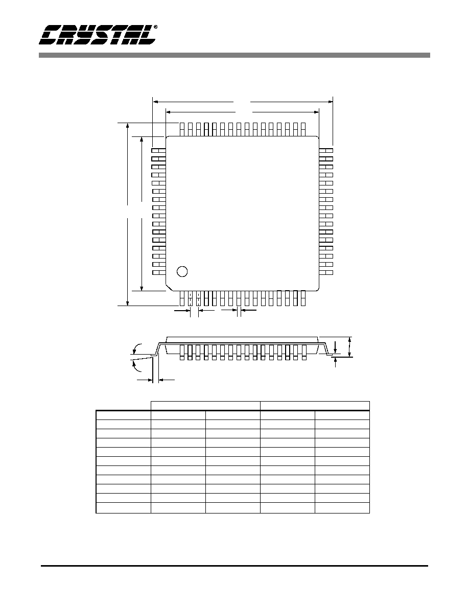
CS7620
68
DS301PP2
6
PACKAGE DIMENSIONS
INCHES
MILLIMETERS
DIM
MIN
MAX
MIN
MAX
A
---
0.063
---
1.60
A1
0.002
0.006
0.05
0.15
B
0.007
0.011
0.17
0.27
D
0.461
0.484
11.70
12.30
D1
0.390
0.398
9.90
10.10
E
0.461
0.484
11.70
12.30
E1
0.390
0.398
9.90
10.10
e*
0.016
0.024
0.40
0.60
L
0.018
0.030
0.45
0.75
0.000∞
7.000∞
0.00∞
7.00∞
* Nominal pin pitch is 0.50 mm
Controlling dimension is mm.
JEDEC Designation: MS026
64L TQFP PACKAGE DRAWING
E1
E
D1
D
1
e
L
B
A1
A

∑ Notes ∑