 | –≠–ª–µ–∫—Ç—Ä–æ–Ω–Ω—ã–π –∫–æ–º–ø–æ–Ω–µ–Ω—Ç: CS7666 | –°–∫–∞—á–∞—Ç—å:  PDF PDF  ZIP ZIP |

Preliminary Product Information
This document contains information for a new product.
Cirrus Logic reserves the right to modify this product without notice.
1
Copyright
©
Cirrus Logic, Inc. 1998
(All Rights Reserved)
Cirrus Logic, Inc.
Crystal Semiconductor Products Division
P.O. Box 17847, Austin, Texas 78760
(512) 445 7222 FAX: (512) 445 7581
http://www.crystal.com
CS7666
Digital Color-Space Processor for CCD Cameras
Features
l
ITU-601 Compliant Image Formatting
l
ITU-656 and SMPTE-125/M Transport
l
Provides Separate HREF and VREF (or
alternately HSYNC and VSYNC) Signals
l
I
2
C Control Interface
l
Limited Secondary I
2
C Bus Master
l
Automatic White Balance
l
Programmable Gamma Correction
l
Programmable Interpolation
l
Programmable Luma Gain and Saturation
Control
l
Fully Programmable Color Separation Matrix
Coefficients
l
Supports up to 1440, active pixels per line,
with no limitation on Vertical Size
l
Pin and software compatible with the CS7665
l
Programmable "Color Killer" circuit
l
Highly integrated for low part count cameras
Description
The CS7666 is a low-power Digital Color-Space Proces-
sor for CCD cameras. It provides all necessary digital
image processing for standard four-color interline trans-
fer CCD imagers. The CS7666 processes the magenta,
yellow, cyan, and green (MYCG) CCD imager data into
YCrCb formatted component digital video. Internal pro-
cessing includes color separation, automatic white
balance, user programmable gamma correction, pro-
grammable scaling (interpolation), and output
formatting. Also, a special "Color Killer" circuit eliminates
false colors during saturation. The digital output of the
CS7666 can be configured to comply with the ITU-601,
ITU-656 and SMPTE-125/M standards. Additionally,
HREF and VREF (or HSYNC and VSYNC) output pins
are provided to support older analog video encoders and
the current ZV-Port definition.
The CS7666 is designed to work directly with the
CS7615 CCD Imager Analog Processor, and is a drop in
replacement for the CS7665.
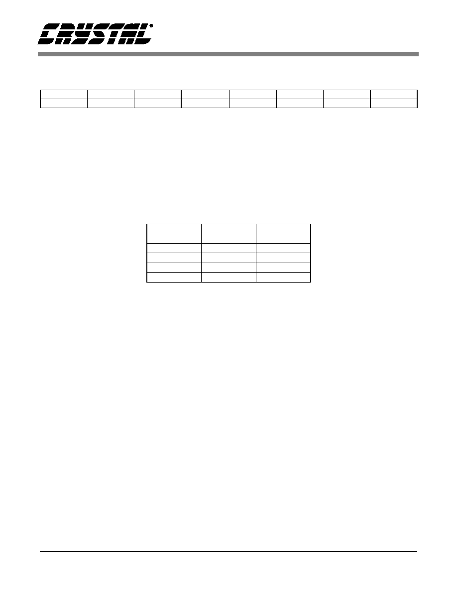
ORDERING INFORMATION
CS7666-KQ
0∞ to 70∞ C
64-pin TQFP
(10 mm x 10 mm x 1.4 mm)
I
DEFORMATTER
COLOR SEPARATION
AND ANITALIASING
WHITE
BALANCE
AWB
CONTROL
GAMMA
CORRECTION
SCALER
OUTPUT
FORMATTER
I
2
C INTERFACE
REGISTER
PLL AND
OUTPUT
BLOCK
CLOCK DRIVER
TIMING
YCrCb
VREF/VSYNC
HREF/HSYNC
XTAL
PRIMARY
I
2
C BUS
SECONDARY
I
2
C BUS
CCD
DATA
DATA
JUL `98
DS302PP1

CS7666
2
DS302PP1
TABLE OF CONTENTS
CHARACTERISTICS AND SPECIFICATIONS ................................................... 3
DIGITAL CHARACTERISTICS.................................................................... 3
SWITCHING CHARACTERISTICS ............................................................. 3
POWER CONSUMPTION ........................................................................... 3
CONTROL PORT CHARACTERISTICS ..................................................... 4
RECOMMENDED OPERATING CHARACTERISTICS............................... 5
ABSOLUTE MAXIMUM RATINGS .............................................................. 5
GENERAL DESCRIPTION .................................................................................. 6
Overview ..................................................................................................... 6
The 640 Pixel Horizontal Line ..................................................................... 7
Embedded ITU-656 EAV and SAV Timing ............................................... 10
Individual Timing and Synchronization Signals ........................................ 11
HREFOUT/HSYNC ................................................................................... 11
VREFOUT/VSYNC ................................................................................... 11
Digital Output Formats .............................................................................. 11
Internal Horizontal Scaler ......................................................................... 14
CLKIN and CLKIN2X Input Timing ........................................................... 14
CLKOUT ................................................................................................... 15
INTERNAL PROCESSING ................................................................................ 15
Input Data Format and Chroma Separator ............................................... 15
Color Saturation Control ........................................................................... 15
White Balance and Gamma Correction .................................................... 15
Chroma Kill ............................................................................................... 16
Internal Filters ........................................................................................... 16
INTERNAL REGISTER STRUCTURE AND USER INTERFACE ..................... 16
Operating CS7666 in Normal I2C Configuration (Three-Byte Mode) ....... 16
Station Address .................................................................................. 17
Write Operations in Three-Byte Mode ................................................ 17
Address Set Operation ....................................................................... 17
Read Operations in Three-Byte Mode ............................................... 17
Operating CS7666 in Four-Byte I2C Configuration ............................ 17
Write Operations in Four-Byte mode .................................................. 18
Read Operations in Four-Byte Mode ................................................. 18
Initializing Slave Devices on Secondary I2C bus from an EPROM .......... 19
Controlling the Configuration Process ...................................................... 19
Reserved Registers and Test Pins ........................................................... 20
PIN DESCRIPTIONS ......................................................................................... 34
Power Supply Connection ........................................................................ 34
Input Data and Clocks .............................................................................. 35
I2C Serial Control ..................................................................................... 35
Digital Video Outputs and Clocking .......................................................... 36
Miscellaneous ........................................................................................... 38
DEFINITIONS ..................................................................................................... 39
PACKAGE DIMENSIONS .................................................................................. 40

CS7666
DS302PP1
3
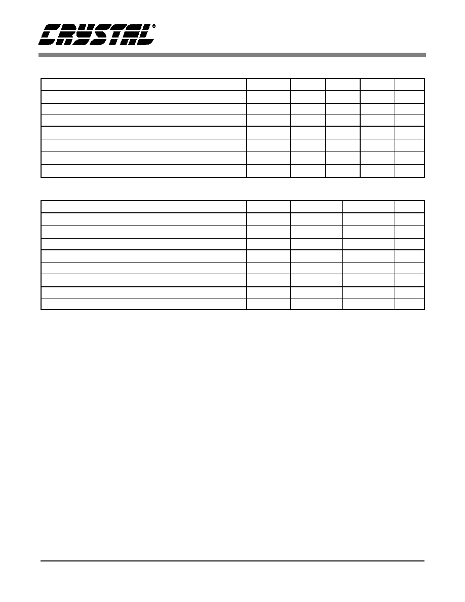
CHARACTERISTICS AND SPECIFICATIONS
DIGITAL CHARACTERISTICS
(T
A
= 25 ∞C; V
DD
= 5 V; C
L
= 30 pF; Input Levels: logic 0 = 0 V, logic 1 = V
DD
.)
SWITCHING CHARACTERISTICS
(T
A
= 25 ∞C; V
DD
= 5 V; C
L
= 30 pF; Input Levels: logic 0 = 0 V, logic 1 = V
DD
.)
Notes: 1. CLKIN, f
CLK
, is f
CLK2X
/2 in non-interpolated mode and f
CLK2X
* 2/5 in interpolated mode.
POWER CONSUMPTION
(T
A
= 25 ∞C; V
DD
= 5 V; C
L
= no load; Input Levels: logic 0 = 0 V, logic 1 = V
DD
.)
Specifications are subject to change without notice
Parameter
Symbol Min Typ
Max
Unit
Logic Inputs
High-Level Input Voltage
V
IH
V
DD
- 0.8
-
-
V
Low-Level Input Voltage
V
IL
-
-
0.8
V
Input Leakage Current
I
IN
-
-
10.0
µA
Input Pin Capacitance
C
DI
-
10
-
pF
Input Clamp Voltage
-
-0.7
-
V
Logic Outputs
High-Level Output Voltage @ I
OH
= 2mA
V
OH
V
DD
- 0.4
-
-
V
Low-Level Output Voltage @ I
OL
= 2mA
V
OL
0.4
-
-
V
High-Z Leakage Current
I
Z
-
-
10.0
µA
Parameter
Symbol Min Typ
Max
Unit
Digital Input
CLKIN2X Frequency Range
(Note 1)
f
CLK2X
-
-
30
MHz
Input Data setup time, DI[9:0]
t
S1
5
-
-
ns
Input Data hold time, DI[9:0]
t
H1
5
-
-
ns
Digital Output
Channel A/B Digital Data Output Clock
Interleaved Data
Parallel Data
f
CLKOUT
-
-
-
-
30
15
MHz
MHz
Channel A/B Output Hold Time
t
OH
-
0
-
ns
Channel A/B Output Propagation Delay
t
PD
-
1.9
5
ns
Digital Output Rise Time with 30 pF load
t
R
-
15
-
ns
Digital Output Fall Time with 30 pF load
t
F
-
15
-
ns
Parameter
Symbol
Min
Typ
Max
Unit
Normal Mode
I
DD
-
80
100
mA
Low Power Mode
I
DD
-
7
16
mA

CS7666
4
DS302PP1
CONTROL PORT CHARACTERISTICS
(T
A
= 25 ∞C; V
DD
= 5 V; Input Levels: logic 0 = 0 V, logic 1 = V
DD
.)
Parameter
Symbol
Min
Max
Unit
SCL Clock Frequency
f
SCL
-
400
kHz
Bus Free Time Between Transmissions
t
buf
1.3
-
µs
Start Condition Hold Time
t
hdst
0.6
-
µs
Clock Pulse Width
High
Low
t
high
t
low
0.6
1.3
-
-
µs
µs
Setup Time for Repeat Start Condition
t
sust
0.6
-
µs
SDAIN Hold Time from SCL Falling
t
hdd
0
-
µs
SDAIN Setup Time from SCL Rising
t
sud
0.1
-
µs
SDAIN and SCL Rise Time
t
r
-
1.0
µs
SDAIN and SCL Fall Time
t
f
-
0.3
µs
Setup Time for Stop Condition
t
susp
0.6
-
µs
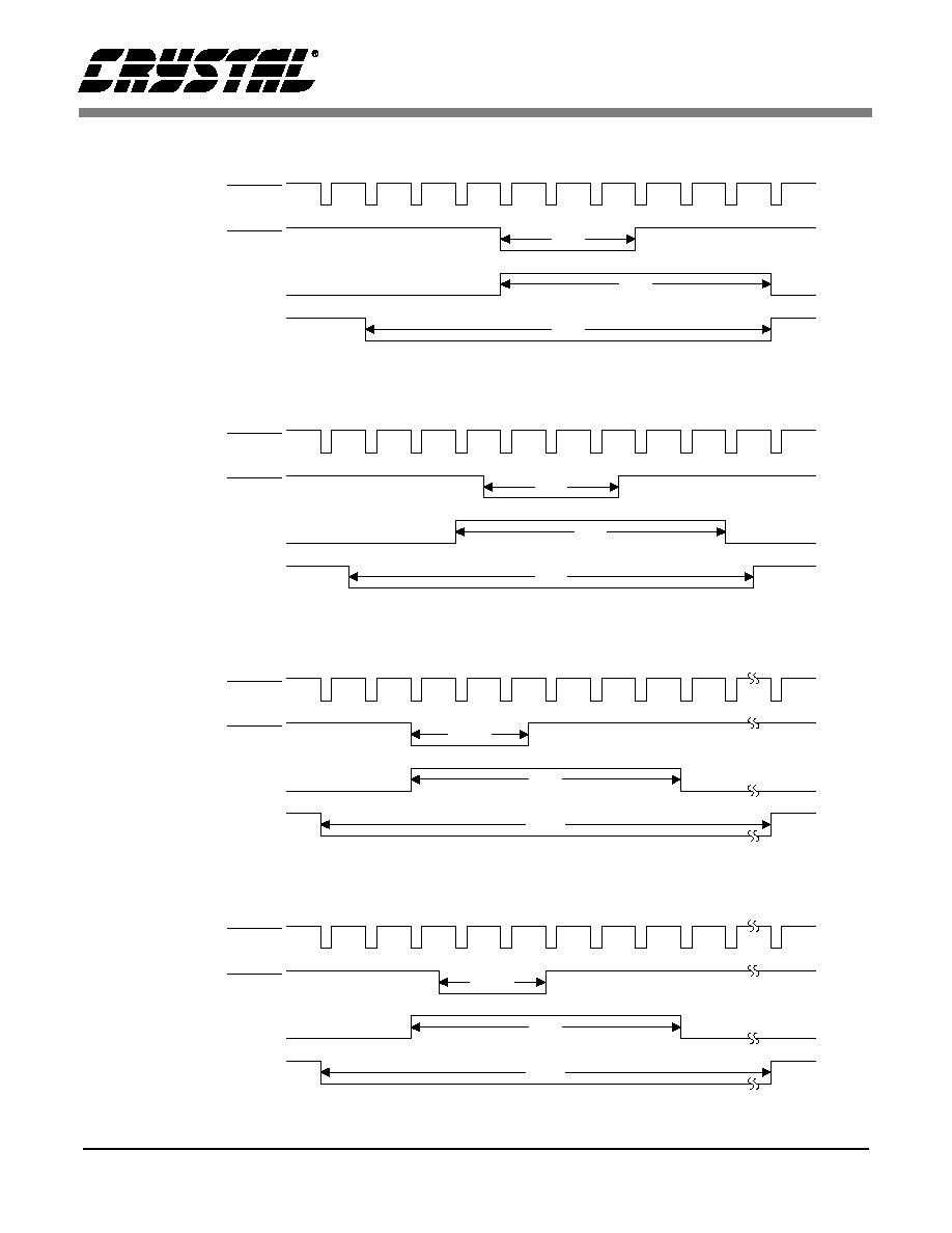
CLKIN2X
CLKIN
Mosaic
Input Data
DI[9:0]
t
H2
t
S2
t
H1
t
S1
CLKOUT
Output Data
DOA[9:0]
DOB[9:0]
t
PD
t
OH
Input Timing Diagram
Output Timing Diagram
t
buf
t
hdst
t hdst
t
low
t
r
t f
t
hdd
t high
t
sud
t
sust
t
susp
Stop
Start
Start
Stop
Repeated
S D A
S C L
I
2
C Timing Diagram
CS7666
DS302PP1
5
RECOMMENDED OPERATING CHARACTERISTICS
ABSOLUTE MAXIMUM RATINGS
WARNING: Operation at or beyond these limits may result in permanent damage to the device.
Normal operation is not guaranteed at these extremes.
Parameter
Symbol Min Typ
Max
Unit
Power Supply Voltage
V
DD
4.5
5.0
5.5
V
Ground to Ground Voltage Differential
-
-
10
mV
Digital Input Rise/Fall Time
-
-
10
ns
CLKIN Level Setup to CLKIN2X Rising (non-interpolated)
t
S2
8
-
-
ns
CLKIN Level Hold after CLKIN2X Rising (non-interpolated)
t
H2
8
-
-
ns
Digital Input Voltage Range
0
-
V
DD
V
Operating Temperature Range
T
A
0
-
70
∞C
Parameter
Symbol
Min
Max
Unit
Power Supply Voltage
V
DD
-0.3
7.0
V
Digital Input Voltage Range
GND - 0.3
V
DD
+ 0.3
V
Forced Digital Output Current
-
50
mA
Sustained Digital Output Voltage
GND - 0.3
V
DD
+ 0.3
V
Output Short Circuit Current
-
-
mA
Operating Temperature Range
T
A
0
70
∞C
Lead Solder Temperature (10 s duration)
-
+260
∞C
Storage Temperature Range
-65
+160
∞C
CS7666
6
DS302PP1
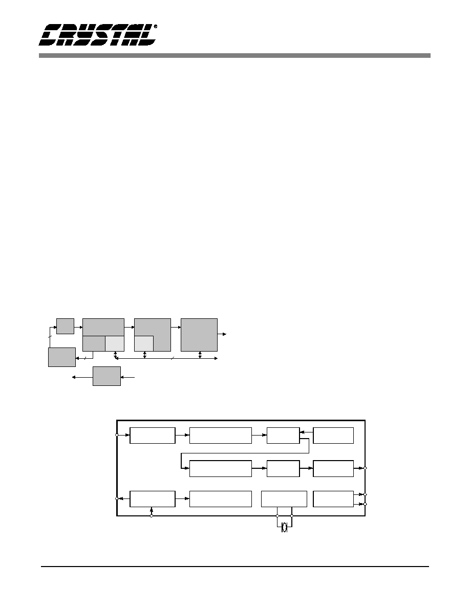
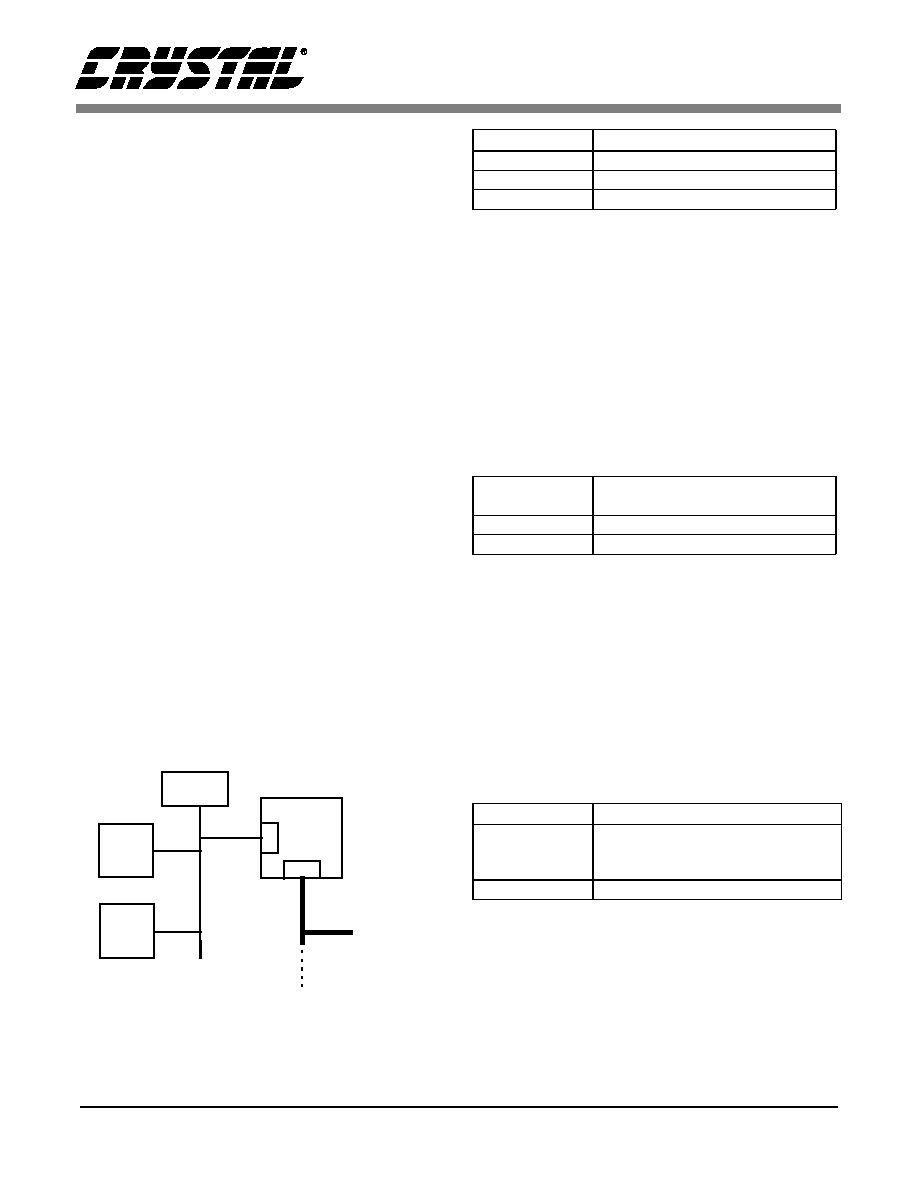
GENERAL DESCRIPTION
Overview
The CS7666 forms the heart of a four chip digital
CCD Camera. The four chips include the CCD im-
ager, the CS7615 CCD digitizer, the CS7666 color
space processor, and a vertical drive interface-chip
for the CCD imager. Most four-phase CCD imag-
ers (and their associated vertical drives) can be
used with the CS7615 digitizer and the CS7666
processor to form a simple and cost-effective
YCrCb output format digital camera. The CS7615
and CS7666 together support imager formats rang-
ing from 175◊175 pixels up to 1000x1000 pixels.
Timing control is located in the CS7615 analog
processor, while the CS7666 synchronizes itself by
decoding the timing cues embedded in the CS7615
data stream. Alternately, the CS7666 accepts hori-
zontal and vertical timing signals on pin inputs.
The block diagram in Figure 1 illustrates a typical
system interconnect.
The CS7666 is a CCD camera color separation and
color-space processor designed to process the four-
color mosaic CCD imager data into ITU-601 com-
pliant 4:2:2 YCrCb digital component video. The
CS7666 timing control is based on the built-in crys-
tal oscillator or on the master clock provided by the
CS7615, and provides formatted component digital
video compliant with SMPTE-125 and ITU-656
transport protocols.
The CS7666 provides color separation of standard
MYCG chroma block data from industry standard
four-color CCD imagers. Gamma correction and
white balance adjustment functions are also includ-
ed in the CS7666. The YCrCb (luminance and
chrominace) data is output at the scaled CCD pixel
rate in 20-bit format, or at twice the scaled pixel
rate in 10-bit format (see discussion on Digital Out-
put Formats). The YCrCb output data from the
CS7666 conforms to the ITU-656 parallel compo-
nent digital video recommendation with embedded
synchronization (see Embedded EAV and SAV
discussion). External horizontal and vertical syn-
chronization signals are also provided to support
ITU-601 interfaces, as well as the PC-Card Zoom-
Video standard being used in notebook computers.
The CS7666 incorporates an internal horizontal
scaler which may be turned on to increase the hori-
zontal pixel count of the popular 360 (CIF) and 512
horizontal pixel per line imagers. The most com-
CCD
Bias
Vertical
Drive
Timing
CDS/ADC
Video
Codec
+18V to +12V
I
2
C
Bus
6
6
2
+5V
CS7666
512x480
CS7615
CCD
Image
Processor
CS4954
I
2
C
I
2
C
Figure 1. Typical 4-Chip Digital CCD Camera
Figure 2. CS7666 Block Diagram
DEFORMATTER
COLOR SEPARATION
AND ANITALIASING
WHITE
BALANCE
AWB
CONTROL
GAMMA
CORRECTION
SCALER
OUTPUT
FORMATTER
I
2
C INTERFACE
REGISTER
PLL AND
OUTPUT
BLOCK
CLOCK DRIVER
TIMING
YCrCb
VREF/VSYNC
HREF/HSYNC
XTAL
PRIMARY
I
2
C BUS
SECONDARY
I
2
C BUS
CCD
DATA
DATA

CS7666
DS302PP1
7
mon target resolutions for the scaler are 640 and
720 pixels per line (square and rectangular pixel
formats), but it is possible to provide generic scal-
ing of M/N where M and N are values from 1 to 31.
The CS7615 and CS7666 chip set supports a wide
range of imager formats while providing an output
format that follows the ITU-601 Component Digi-
tal Video recommendation. The ITU-601 docu-
ment primarily specifies horizontal resolutions of
720 active horizontal pixels (which is required for
broadcast television compatibility). However,
many of today's digital video receivers are capable
of operating with a wide range of video image for-
mats. Even though these digital video receivers al-
low image formats not specified in the ITU-
601/656 recommendation, all of these receivers ex-
pect the basic ITU-601/656 protocol to be followed
in terms of data sequence and timing cues. This is
the case with the CS7666, where all output formats
follow the ITU-601/656 recommendation even if
the image formats differ in horizontal and vertical
pixel dimensions.
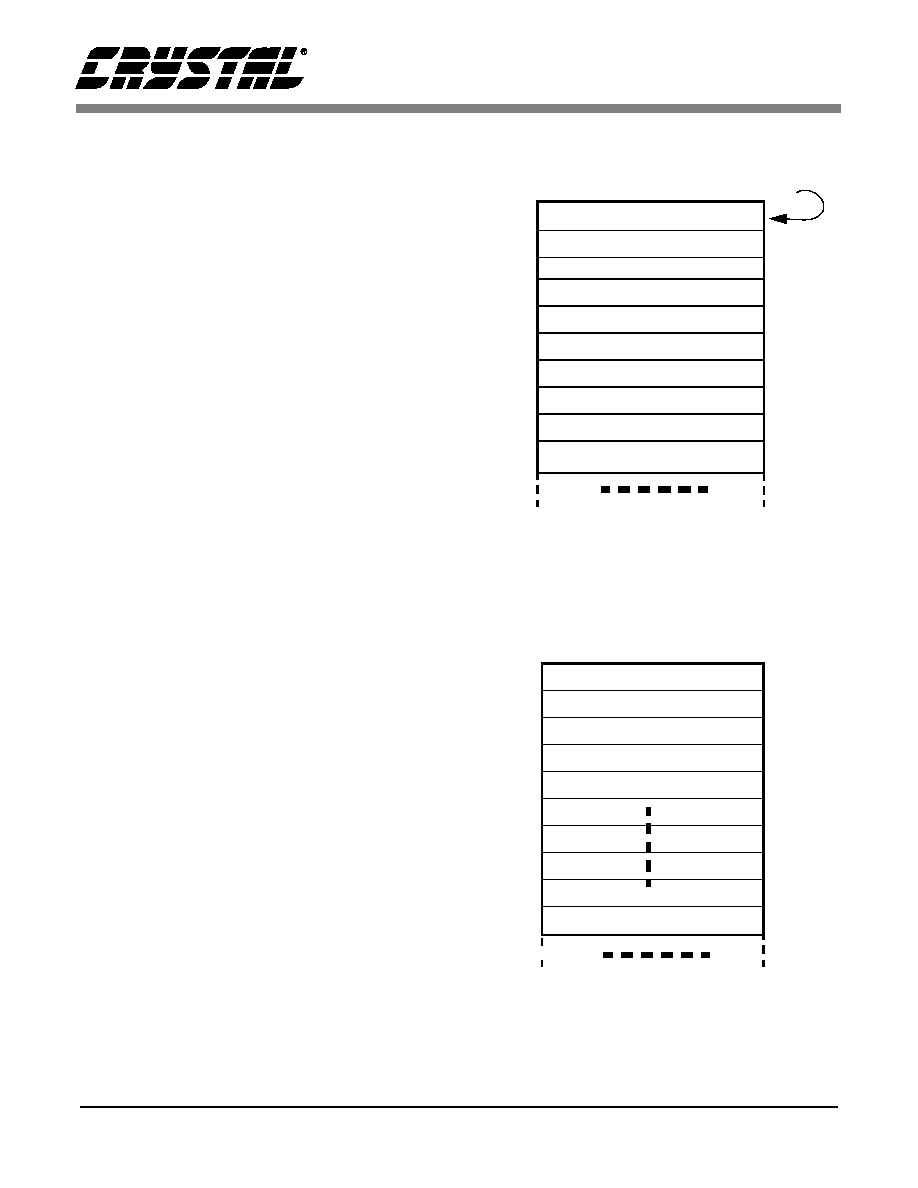
The 640 Pixel Horizontal Line
The following discussion assumes that a 512 hori-
zontal pixel class imager has been selected for the
camera, the CS7615 has been programmed to pro-
vide 512 active pixels and 112 inactive pixels, and
that the internal 4:5 horizontal scaler has been en-
abled (scaler mode 1). Many other imager/scaler
combinations are possible, but the digital video for-
mat would not be significantly different than the
640x480 case described.
Transmitted during each active line are 1280 mul-
tiplexed luminance and chrominance values (640
luminance, 320 chrominance Cr, and 320 chromi-
nance Cb values). Eight of the remaining 280 inter-
face clock intervals are used to transmit
synchronizing information. The first of these 1560
interface clock intervals is designated line 0 word 0
for the purpose of reference only. The 1560 sample
words per total line are therefore numbered 0
through 1559. Intervals 0 through 1279, inclusive,
contain video data.
The interface clock intervals occurring during dig-
ital blanking are designated 1280 through 1559. In-
tervals 1280 through 1283 are reserved for the end-
active-video (EAV) timing reference. Intervals
1556 through 1559 are reserved for the start-of-ac-
tive-video (SAV) timing reference. Figure 3 indi-
cates the values of the timing reference signals (F,
V, H) for an entire frame of interlaced video. Please
note the scan lines are numbered 1 through 525
consecutively in the time domain (spatially they are
interlaced). Table 1 defines the 1560 samples of a
single scan line of video.

CS7666
8
DS302PP1
Vertical Blanking
Vertical Blanking
H
o
r
i
z
ont
a
l
Bl
a
n
k
i
n
g
Ho
ri
zo
n
t
a
l
B
l
ankin
g
Active Video
Field 1
Active Video
Field 2
EAV
H=1
SAV
H=0
64
0
77
9
0
63
9
F=1
Lines
266 to 3
F=0
Lines
4 to 265
Lines 1 to 19 V=1
Lines 20 to 263
V=0
Lines 264 to 282 V=1
Lines 283 to 525
V=0
Figure 3. Horizontal and Vertical Timing States
(640◊480 resolution)
CS7666
DS302PP1
9
Word
Data Content
Pixel
Notes
1280
1111
1111
640
EAV
1281
0000
0000
EAV
1282
0000
0000
EAV
1283
1FV1
P3P2P1P0
641
EAV
1284
1000
0000
642
Fro pixels 642 to 777
Cr = Cb = 80h
Y = 10h
1285
0001
0000
1286
1000
0000
1287
0001
0000
643
1552
1000
0000
776
1553
0001
0000
1554
1000
0000
1555
0001
0000
777
1556
1111
1111
778
SAV
1557
0000
0000
SAV
1558
0000
0000
SAV
1559
1FV0
P3P2P1P0
779
SAV
0
Cb0
0
Start of Digital Video
1
Y0
For VBLANK line 1 to 19
and 264 to 283
Cr = Cb = 80h
Y = 10h
2
Cr0
3
Y1
1
4
Cb2
2
5
Y2
6
Cr2
7
Y3
3
2n
Cbn
n
For active pixels 20
through 263 and 283 to
525 for n=even from pix-
els 0 to 638
2n + 1
Yn
2n + 3
Crn
Yn+1
n+1
1272
Cb636
636
1273
Y636
1274
Cr636
1275
Y637
637
1276
Cb638
638
1277
Y638
1278
Cr638
1279
Y639
End of Digital VIdeo
Table 1. Detail of Scan Line for 640x480 Image

CS7666
10
DS302PP1
Embedded ITU-656 EAV and SAV Timing
The lines in Figure 3 are numbered 1 through 525.
Video data is not present on lines 1 to 19 or 264 to
282, which constitute the vertical blanking periods.
The vertical blanking is in full line increments,
where Y samples are set to 10h, while Cb and Cr
samples are set to 80h. The interval starting with
EAV and ending with SAV is the digital horizontal
synchronization, which occurs on every line.
It is implicit that the timing reference signals are
contiguous with the video data and continue
through the vertical blanking interval. Each timing
reference signal consists of the four-word sequence
in Table 2. The first three words are a preamble,
followed by a fourth word indicating a) even field
(field 2) identification, b) state of vertical blanking,
and c) state of horizontal blanking. Table 1 details
the timing reference format. The protected bit
states are dependent on the F, V, and H bits accord-
ing to Table 3.
Protected State Bits - In Tables 3 and 4, H, V, and
F bits provide all the necessary timing and state in-
formation. Bits 0 to 3 provide error detection and
correction information. The protection bits allow
for correction of single-bit errors and detection of
two-bit errors. The F or field bit indicates which of
the interlaced fields is active, the first/odd field
which contains 262 lines, or the second/even field
which contains 263 lines.
Value
Description
First Byte
FFh
Fixed
Second Byte
00h
Fixed
Third Byte
00h
Fixed
Fourth Byte
xyh
See Table 3
Table 2. Timing Reference Signal
Bit Position
Word 1281
and 1556
Word 1281
and 1557
Word 1282
and 1558
Word 1283
and 1589
Description
7
1
0
0
1
Fixed
6
1
0
0
F
F = 0 during Field 1/ODDF = 1
during Field 2/EVEN
5
1
0
0
V
V = 0 during Active VideoV = 1
during Vertical Blanking
4
1
0
0
H
H = 1 at end of Active VideoH = 0
at start of Active Video
3
1
0
0
P3
see Protected Bits State Table 4
2
1
0
0
P2
see Protected Bits State Table 4
1
1
0
0
P1
see Protected Bits State Table 4
0
1
0
0
P0
see Protected Bits State Table 4
Table 3. EAV and SAV Timing Reference Signal Detail.
Bit 7
Bit 6 (F)
Bit 5 (V)
Bit 4 (H)
Bit 3 (P3)
Bit 2 (P2)
Bit 1 (P1)
Bit 0 (P0)
1
0
0
0
0
0
0
0
1
0
0
1
1
1
0
1
1
0
1
0
1
0
1
1
1
0
1
1
0
1
1
0
1
1
0
0
0
1
1
1
1
1
0
1
1
0
1
0
1
1
1
0
1
1
0
0
1
1
1
1
0
0
0
1
Table 4. EAV and SAV Protected Bit States Detail.

CS7666
DS302PP1
11
Individual Timing and Synchronization
Signals
In addition to the embedded EAV and SAV timing
signals, the CS7666 provides individual synchroni-
zation output signals which are employed by many
video encoder circuits. These synchronization sig-
nals are typically used to interface the ITU-656 dig-
ital video stream to other components and
subsystems. The individual synchronization sig-
nals include HREFOUT and VREFOUT.
HREFOUT/HSYNC
HREFOUT is an active-high signal indicating
when active pixel data is being transmitted on
DOA[9:0] or DOB[9:0]. HREFOUT is low when
non-active picture data is being transmitted during
horizontal blanking. Depending on the mode of op-
eration, the HREFOUT signal follows either the
HREFIN signal or the HREF defined by the EAV
and SAV code.
The HREFOUT pin may also be configured to pro-
vide a HSYNC output that provides an active low
pulse for 64 pixel clocks whose falling edge occurs
16 pixel clocks after the end of active video for
NTSC (12 clocks for PAL) as per the ITU-R
BT.601 specification. HSYNC is chosen by setting
the Operation Control Register II (07h) HS_SEL
bit (bit 0) to a value of 1. This pin may be inverted
by setting the H_INV bit (register 07h bit2) to a
value of 1. The HSYNC signal may be delayed by
0, 0.5, 1, or 1.5 pixel clocks by setting H_SFT[1-0]
appropriately (register 07h bits 5 and 4.)
VREFOUT/VSYNC
VREFOUT is an output signal that is active high
when the CS7666 is putting out active video lines.
The active-low portion of this signal defines the
vertical blanking period. If the VS_SEL bit in reg-
ister 07h is set, this output pin produces a vertical
sync signal that is compatible with current PAL or
NTSC analog systems. See Figure 4. This signal is
active for 3 line times in NTSC mode (bit 5 of reg-
ister 04h = 0) and 2.5 line times in PAL mode (bit5
of register 04h = 1.) This line may be inverted by
setting the V_INV bit (register 07h) to a value of 1.
Alternately, when the ZV mode bit in register 06h
is set, this output behaves as a VSYNC signal ap-
propriate for ZV ports. In the ZV mode, the
VSYNC signal is active-high during the first six
horizontal line periods of every field. The transition
in VSYNC signal lags the HREF signal's rising
edge during odd fields and leads the rising edge of
HREF during even fields.
Digital Output Formats
The CS7666 outputs data in a 20-Bit wide format at
the output pixel clock rate. Alternately, the data can
be multiplexed in a 10-bit format at a 2x output pix-
el clock rate. Figures 5 and 6 detail the clock and
data relationships. The output data transitions on
the falling edge of the clock such that the rising
edge of the clock can be used to latch the data into
subsequent circuitry.
The CS7666 delivers 4:2:2 component digital vid-
eo output data in YCrCb format. The data conforms
to the ITU-R BT.656 specification. The Y compo-
nent range is 16-235 (8-bit data) and the Cr and Cb
component ranges are 16-240 (8-bit data). Howev-
er, by setting CLIP_OFF (register 07h bit 6) to a
value of 1, the output data can be extended to a
range of 1-254 (8-bit data). Only 00 and FF are re-
stricted to allow digital timing codes.
The digital outputs can be configured for 10-bit in-
terleaved Y and CrCb data, or for 20-bit parallel
operation. The INTERL bit of the Operational Con-
trol Register 06h determines which output format is
active. Logic 0 places the CS7666 in interleave
mode with output data on channel "A." Logic 1
places the CS7666 in non-interleaved mode where
luminance data is output on channel "A" and
chrominance data is output on channel "B."
CS7666
12
DS302PP1
HSYNC
VSYNC
VREF
3H
6H
9H
525
1
2
3
4
5
6
7
8
9
10
VSYNC ZV Mode
Line
NTSC Vertical Timing (odd field)
HSYNC
VSYNC
VREF
3H
9H
263
264
265
266
267
268
269
270
271
272
273
VSYNC ZV Mode
Line
NTSC Vertical Timing (even field)
HSYNC
VSYNC
VREF
624
625
1
2
3
4
5
6
7
23
VSYNC ZV Mode
Line
PAL Vertical Timing (odd field)
HSYNC
VSYNC
VREF
311
312
313
314
315
316
317
318
319
336
VSYNC ZV Mode
Line
PAL Vertical Timing (even field)
6H
2.5H
6H
24H
25H
6H
2.5H
Figure 4. Vertical Timing

CS7666
DS302PP1
13
24.5454MHz
CLKOUT
DO [9-0]
Line 3 Pixel 776
to Line 4 Pixel 3
DO [9-0]
Line 263 Pixel 638
to Line 264 Pixel 645
DO [9-0]
Line 525 Pixel 638
to Line 1 Pixel 645
Cb638
Y638 Cr638
Y639
FFh
00h
00h
9Dh
80h
10h
80h
10h
80h
10h
EAV
FFh
00h
00h
F1h
80h
10h
80h
10h
80h
10h
80h
10h
80h
10h
EAV
FFh
00h
00h
ABh
80h
10h
80h
10h
80h
10h
80h
10h
80h
10h
SAV
A
A
A
NOTE: EAV, SAV, and Blanking data values are based on the 8 MSB's of the output data, the two LSBs are considered fractional.
Figure 5. 2x Pixel Clock, 10-Bit interleaved Output Format for 640x480 Image Format.
12.2727MHz
CLKOUT
HREF
DO [9-0]
DO [9-0]
10h
Y0
Y1
Y2
Y3
Y4
Y633
Y634
Y635
Y636
Y637
Y638
Y639
10h
80h
Cb0
Cr0
Cb2
Cr2
Cb4
Cb632 Cr634 Cb634 Cr636 Cb636
Cr638
Cb638
80h
A
B
NOTE: EAV, SAV, and Blanking data values are based on the 8 MSB's of the output data, the two LSBs are considered fractional.
Figure 6. 1x Pixel Clock, 20-Bit Parallel Output Format for 640x480 Image Format.

CS7666
14
DS302PP1
In 20-bit wide mode, the luminance information is
output on DOA[9:0] and the chrominance informa-
tion is output on DOB[9:0].
The CS7666 supports both 8-bit and 10-bit opera-
tion as per the ITU-656 recommendation. The ITU-
656 recommendation defines the primary data path
as 8-bits wide with two additional fractional bits
that can be used to form a 10-bit data path. If only
8-bits of output data are used, the two LSBs, DOA1
and DOA0 (DOB1, DOB0) are not used. However,
DOA[9:2] (DOB[9:2]) are connected exactly the
same as in a 10-bit system. This is essential to
properly pass the image data and synchronization
signals to the next component.
Internal Horizontal Scaler
The internal horizontal scaler is used to bridge be-
tween common CCD imager formats and computer
or television formats. In the CS7665 compatibility
mode (default after reset) a 4:5 data rate scaler is
selected by setting the INTERP pin (pin 54 on the
CS7666) to a logical one. The 4:5 scaler will con-
vert a standard 512 horizontal pixel width CCD im-
ager used for cam-corders into the VGA 640x480
format. The CS7615 (if that device is used in the
system) must also have its INTERP pin set high.
When the CS7666 is in the native CS7666 mode
(True_7666 in register 04h set to 1), the INTERP
pin is ignored and the internal scaling ratio is pro-
grammed by the user. The CS7615 must have its
INTERP pin tied to ground.
Several pre-defined scaler modes may be selected
by writing a 3-bit value to bits 0-2 of register 04h.
These default scaling modes are described in
Table 7. If the CUSTOM bit (bit 3 of register 04h)
is set to a 1, then the scaling ratio is determined by
the M and N values contained in the Scaler Control
registers (2Dh - 2Fh.)
CLKIN and CLKIN2X Input Timing
The CLKIN, pin 55, will always require a primary
pixel rate clock source. CCD manufacturers gener-
ally specify a pixel clock frequency that is compat-
Parallel
INTERL = 1
Interleaved
INTERL = 0
DOA[9:0]
10-Bit
Luminance Data
Interleaved 10-Bit
Luminance Data
and 10-Bit
Chrominance Data
DOB[9:0]
10-Bit
Chrominance Data
0
CLKOUT
Pixel Rate
2x Pixel Rate
Table 5. INTERL Controlled Output Formats
Register 04h
bit 4
Pin 54
Operation
Scaling Ratio
0
0
CS7665 mode
1:1
0
1
CS7665 mode
4:5
1
X
CS7666 mode programmable
Table 6. INTERP Pin (Pin 54)
Mode
CCD Format
CCD Clock (MHz)
Output Format
Input Clock (MHz)
Scaling Ratio
000
CCD
Ω input clock
same as CCD
(30 MHz max.)
1:1
001
512x480
9.818
640x480
24.5454
4:5
010
512x480
9.346
720x480
27.000
9:13
011
512x576
9.281
720x480
27.000
11:16
100
362x480
6.75
640x480
24.5454
11:20
101
362x480
6.75
720x480
27.000
1:2
362x576
6.75
720x576
27.000
110
512x576
9.563
720x576
27.000
17:24
111
512x480
9.000
720x480
27.000
2:3
512x576
9.000
720x576
27.000
Table 7. Default Scaling Modes (Register 04h)

CS7666
DS302PP1
15
ible with one of the analog encoders that can be
used with a given imager. If an analog encoder is
used in the camera to generate an analog output, the
pixel clock frequency expected by the encoder
must be matched precisely. However, digital dis-
play systems, such as those based on VGA graphics
adapter cards and Zoom Video systems, are gener-
ally not sensitive to pixel clock frequency, and will
tolerate a wide range of pixel and frame rates.
Specific pixel-rate clock frequencies for analog en-
coders include 14.31818 MHz for 768H imagers,
the primary ITU-601 13.5 MHz for 720H imagers,
and down to 12.272727 MHz clock rates for 640H
VGA format imagers.
In CS7665 compatibility mode (register 04h bit 4 =
0), The CLKIN2X, pin 56, will either require a
2.5X CCD pixel rate clock when the internal 4:5
scaler is enabled (INTERP pin high) or a 2x times
the CCD pixel rate clock in non-interpolation
mode (INTERP pin low). The CLKIN2X pin is
used as a crystal input pin when the CS7666 is in
native mode (register 04h bit4 = 1).
CLKOUT
CLKOUT follows the output data rate as described
in the Digital Output Formats section. In the non-
interleaved mode the clock output is at the output
luma sample rate whereas in the interleaved mode
the clock output is at 2x the output luma sample
rate.
INTERNAL PROCESSING
The internal operation of the CS7666 can be sepa-
rated into several distinct blocks. The following
section provides an overview of how these blocks
operate and interact.
Input Data Format and Chroma Separator
The CS7666 accepts up to 10-bit MYCG image
data from a CCD digitizer such as the CS7615.
suitable CCD analog processing unit. The CS7666
internally converts the four-color CCD MYCG in-
terlaced image data into the various color space for-
mats. These include RGB and YUV, as well as
YCrCb. The individual image adjustments are per-
formed in the most appropriate color space repre-
sentation. Ultimately the image is converted to
YCrCb format for outputting data.
Color Saturation Control
Color saturation control is via the Red Saturation
and the Blue Saturation control register addresses
0Ah and 0Bh.
White Balance and Gamma Correction
The red and blue color balances can be adjusted
through the I
2
C control port. During the AWB (au-
tomatic white balance) sequence the red level is ad-
justed to minimize the (Y-R) difference
component; similarly the blue level is adjusted to
minimize the (Y-B) color difference component.
An automatic white balance is initiated by writing
a 1 to register 05h bit 1. For manual control, the red
balance is accessed through register 08h, and the
blue balance is accessed through register 09h.
Gamma correction is provided to offset the non-lin-
ear illumination profile of the display device. Sep-
arate 256 entry tables are supplied for red, green,
and blue. Each entry is 8-bits. The gamma table is
programmed through register 0Ch. The write for-
mat is similar to the write format described in the
normal I
2
C operation section later in this docu-
ment. The first byte contains the CS7666 device
address and write bit, the second byte contains the
CS7666 gamma table register address (0Ch), the
third byte determines which gamma RAM to up-
date (red, green, and blue), the next 256 bytes con-
tain the gamma table entries.
The blue gamma RAM is selected by setting regis-
ter 0Ch bit 0 to a one; the green gamma RAM is se-
lected by setting register 0Ch bit 1 to a one; and the
red gamma RAM is selected by setting register 0Ch
bit2 to a one. Any, or all of the gamma RAMs may
be selected . The most common implementation is

CS7666
16
DS302PP1
to write the same gamma table to all 3 RAMs by
setting bits 0-2 high. The gamma table itself is
loaded from low to high. The first byte after the
RAM selection byte will correspond to the value
used when the input data is 00h, the 256th byte after
the RAM selection byte will correspond to the val-
ue used when the input data is FFh.
The gamma table is read in a similar manner. How-
ever, certain restrictions are made to reads. First,
the gamma RAMs may only be read one at a time
(RAM selection byte = 01,02,04 only) and, second,
the gamma table may only be read when gamma
correction is disabled (register 05 bit2 = 0).
Chroma Kill
As the brightness of an image increases, the green,
yellow, cyan, and magenta pixels within the CCD
array will saturate at different intensity levels. As a
result, a highly illuminated object or light source
may start to look cyan. To overcome this effect, an
internal Chroma killer circuit compares the luma
and chroma values of each pixel to a set of pro-
grammable thresholds. If the pixel's luma value is
greater than the Y_THR value (register 27h) and its
Cr and Cb values are between the CR_THR_H ,
CR_THR_L , CB_THR_H, and CB_THR_L
threshold values respectively, then that pixel will
lose its chroma value (become white.) These
thresholds are stored in registers 27h - 2Ch.
Internal Filters
The CS7666 has an internal low-pass chroma filter
to reduce the effects of color aliasing. This filter is
enabled by writing a value of 0 to bit 4 of register
05h. The CS7666 also contains a luma peaking fil-
ter to enhance the edges of blurred images. This fil-
ter is enabled by setting register 05h bit 3 to a value
of 0.
INTERNAL REGISTER STRUCTURE
AND USER INTERFACE
The user interface describes the user's external
view of the CS7666 and the basic control opera-
tions. These areas include digital data output modes
and organization, timing and synchronization sig-
nals, I
2
C interface, and miscellaneous controls.
The CS7666 has two I
2
C ports: (1) a slave I
2
C port
called the primary I
2
C port, and (2) a secondary I
2
C
port with limited I
2
C master capabilities. The pri-
mary I
2
C port allows an external controller to con-
trol the CS7666. It is assumed the external
controller will also directly control any other I
2
C
slave devices on the camera board. This is the nor-
mal I
2
C operation mode of CS7666. The secondary
I
2
C port, on the other hand, may be used to control
all the other slave devices on a camera board
through the CS7666 only. This feature is useful
when the external I
2
C controller is used to control
multiple cameras. When used in this configuration
the 4BYTEMODE pin (pin 1) of the CS7666 must
be tied high and the device is operated in four-byte
mode.
Operating CS7666 in Normal I
2
C
Configuration (Three-Byte Mode)
In normal mode, the CS7666 is connected as a
slave device to an external I
2
C controller through
the primary I
2
C port. The connection is done via a
two-wire serial bus. Other I
2
C devices on the cam-
era may also share the same serial bus. The external
controller communicates with the I
2
C devices by
sending and receiving short packets of 8-bit words
in accordance with the I
2
C protocol. The packets
contain the station address of the target device, the
desired register address, and data.
There are three packet formats: WRITE format,
ADDRESS SET format, and READ format. Each
packet is addressed to a device by the station ad-
dress. The LSB of the station address is the R/W
(data direction) bit. This bit is set LOW in the
WRITE and ADDRESS SET packets, and it is set
CS7666
DS302PP1
17
HIGH for READ packets. The master can read and
write to non-existent registers within the selected
device. WRITE operations will have no effect;
READ operations will return a value of 00h.
Station Address
Each device on the I
2
C bus has a unique 7-bit ad-
dress. An eighth bit, the R/W bit, determines if the
current data transfer writes data to the slave device
or reads data from the slave device. It is common to
represent the station address and R/W bit as two 8-
bit station addresses, one address for write accesses
and another address for read accesses. We will fol-
low this practice. The CS7666 default station ad-
dress is 34h for writes and 35h for reads. The
station address can be changed by writing a new
station address to register FFh. The value written to
this register does not include the R/W bit. For ex-
ample. The default station address (34h write / 35h
read) will be stored as 1Ah in register FFh.
Write Operations in Three-Byte Mode
The WRITE format consists of a three-byte packet.
The first byte is the station address with the data di-
rection bit set LOW to indicate a write. The second
byte is the device register address (0..255). The
third byte is the register data (0..255). No addition-
al bytes are allowed.
Address Set Operation
The ADDRESS SET format consists of a two-byte
packet which sets the address of a subsequent
READ operation. The first byte of the Station Ad-
dress with the LSB (data direction bit) set LOW to
indicate a write operation. The second byte is the
register address (0..255). The ADDRESS SET for-
mat is the same as the WRITE format, without the
register data (third byte).
Read Operations in Three-Byte Mode
The READ operation may consist of two or more
bytes. The first byte is the station address with the
LSB (data direction bit) set HIGH indicating a read
operation. The addressed device then sends one or
more bytes back from the register last addressed by
the previous WRITE operation or the previous AD-
DRESS SET operation.
Operating CS7666 in Four-Byte I
2
C Config-
uration
In this configuration the external controller talks
only to the CS7666 through the primary I
2
C inter-
face. All the other slave devices on the camera
External
EPROM
secondar
y
I
2
C
pri
m
ar
y I
2
C
CS7615
CS7666
controller
CS4954
Figure 7. I
2
C configuration showing primary
and secondary I
2
C busses.
To other sub-systems
Byte Sequence
WRITE Format Packet Detail
First Byte
Station Address with LSB Set LOW
Second Byte
Device Register Address (0..255)
Third Byte
Register Data (0..255)
Table 8. WRITE Format Packet
Byte Sequence
ADDRESS SET format
Packet Details
First Byte
Station Address with LSB Set LOW
Second Byte
Device Register Address (0..255)
Table 9. ADDRESS SET Format Packet Operation
Byte Sequence
READ Format Packet Details
First Byte
Station Address with LSB set HIGH;
Source Device then Returns One
Byte of Register Data (0..255)
Second Byte
Returned data from CS7666
Table 10. READ Format Packet.

CS7666
18
DS302PP1
board are tied to the secondary I
2
C port of the
CS7666. WRITE and READ packets only are de-
fined in four-byte mode. Independent address set
operations to slave devices on the secondary I
2
C
bus is not allowed in four-byte mode. Four-byte
mode is active when the 4BYTEMODE pin (pin 1)
is logic high.
Write Operations in Four-Byte mode
All WRITE operations from an external controller,
through the CS7666, to any slave device must use
the four-byte mode; this includes writing to the
CS7666 itself. The external controller sends a four-
byte WRITE command to the CS7666 which ini-
tiates a WRITE operation to the destination slave
device and sets the I2CBUSY bit in the status reg-
ister (01h). The I2CBUSY bit is cleared when the
write operation on the secondary bus is complete.
The External controller can poll the status register
to check if the CS7666 has completed the com-
mand.
The CS7666 has a one command buffer which al-
lows the external controller to queue one additional
command while the current command is still being
executed. If more than one command is sent before
the I2CBUSY bit is cleared, the CS7666 saves only
the last command and executes it after the current
one is completed. Commands that involve writing
or reading only to CS7666 registers are not put in
the queue but are executed immediately without af-
fecting any transactions occurring on the master
I
2
C interface.
Any attempt by the external I
2
C controller to write
to the CS7666 registers while the CS7666 is busy
initializing from an external EEPROM will be ig-
nored. However, reads from the CS7666 are al-
lowed during this time.
If, during a READ or WRITE operation to a slave
device, the CS7666 fails to receive an acknowledge
bit the execution of the command is aborted and the
NODEV bit in the status register is set high. This
bit remains set unless it is explicitly cleared by
writing to it or a new command is written to
CS7666.
Read Operations in Four-Byte Mode
The READ operation in four-byte mode first re-
quires a three-byte READ-TRIGGER packet to the
CS7666. The first byte is the station address of the
CS7666 with the LSB set LOW. The second byte is
the target slave device's station address with the
LSB (data direction bit) set HIGH. The third byte is
the register address (0..255).
The READ-TRIGGER packet initiates a READ
operation by the CS7666 from the target slave de-
vice on the secondary I
2
C bus. The status register
in the CS7666 may be checked to see if the read op-
eration has been completed. The I2CBUSY bit in
status register 01h is set to zero when the operation
is completed.
On completion of a read cycle from the target de-
vice, the CS7666 places the data read into the Slave
Data Hold register at address 19h. The external
controller can read this data through the primary
I
2
C port. This requires first performing an AD-
DRESS SET operation to set the address to 19h and
Byte Sequence
WRITE Format Packet Detail
First Byte
Station Address of CS7666 with LSB
Set LOW
Second Byte
Station Address of target slave
device with LSB Set LOW
Third Byte
Device Register Address (0..255)
Fourth Byte
Register Data (0..255)
Table 11. Four-byte WRITE Format Packet
Byte Sequence
READ-TRIGGER format Packet
Details
First Byte
CS7666 Station Address with LSB
Set LOW
Second Byte
Target device Station Address with
LSB Set HIGH
Third Byte
Device Register Address (0..255)
Table 12. READ-TRIGGER packet in four-byte mode
CS7666
DS302PP1
19
then sending a one-byte station address indicating
read to the CS7666. The data from register 19h is
then returned by the CS7666.
Initializing Slave Devices on Secondary I
2
C
bus from an EPROM
An EPROM may be attached to the secondary I
2
C
bus for initialization purposes. Resetting the
CS7666 initiates a download of register values
from the EPROM into any of the slave devices on
the secondary I
2
C bus. The EPROM is assumed to
be at station address A0h. If during initialization,
the CS7666 does not receive an acknowledge bit
from the EPROM, all transactions with the
EPROM are aborted and the NODEV status bit is
set in status register at address 01h.
The data within the EPROM is formatted in three-
byte packets that represent the destination address,
register address, and data. After reading a packet,
the CS7666 initiates an I
2
C bus cycle using the first
byte as the device station address, the second byte
as the device register address, and the third byte as
the data being written to the device. If an acknowl-
edge is received from the target device, the CS7666
will fetch the next 3 bytes from the EPROM and re-
peat the process. The only exception being the
gamma table whose entire 256 bytes is transferred
in one I
2
C write cycle. This process will continue
until the total number of packets read equals the
value in the EEPROM count register (registers 1Ah
and 1Bh), a HALT command is executed, or no ac-
knowledge is received from the target device.
While the CS7666 is downloading from the
EPROM, the INITACT bit (register 01h bit3) is set
in the status register of CS7666. All attempts to
write to CS7666 registers by an external controller
will be ignored during this time.
Controlling the Configuration Process
The simplest configuration would consist of an
EPROM with one configuration file. In this case,
the first commands in the EPROM should write the
total number of packets in the EEPROM. This data
is written to the EEPROM count high and low byte
registers (registers 1Ah and 1Bh). Subsequent
bytes would contain all the necessary data to con-
figure the camera. This data will be read in a se-
quential fashion.
If, however, multiple configurations are desired,
the EEPROM may be programmed with multiple
sets of data, and the CS7666 programmed to select
one of 8 configurations. The CS7666 incorporates
3 commands to handle multiple configurations:
SKIP, JUMP, and HALT.
The SKIP command tells the CS7666 to skip to the
address within the EEPROM specified by the Con-
figuration Control registers (30h - 3Fh). The Con-
figuration Control registers are used in pairs to
provide a 11-bit EEPROM address. The Configura-
tion Index register determines which two of the 8
pairs will be used.
The Configuration Index Register is loaded auto-
matically after reset by the CS7666. The CS7666
will attempt a read cycle from the parallel I/O port
of a Crystal CS495X series video encoder or
SAA8574 I
2
C port expander from Philips Semi-
conductors. If the read cycle is successful, the Con-
figuration Index register will contain the state of
the lower 3 bits of the parallel I/O port. If both the
Byte Sequence
WRITE Format Packet Detail
First Byte
Station Address of CS7666 with
LSB Set LOW
Second Byte
Station Address of CS7666 with
LSB Set LOW
Third Byte
Slave Data Hold reg. address 19h
Table 13. Address Set for Slave Data Hold register in
Four-byte mode
Byte Sequence
READ Format Packet Details
First Byte
CS7666 Station Address with LSB
set HIGH.
Second Byte
Returned data from register 19h of
CS7666
Table 14. READ Format Packet.
CS7666
20
DS302PP1
SAA8574 and a CS495X series part are present, the
CS495X series part I/O port value will be used. A
set of shunts or DIP switches attached to the I/O
port provides a convenient way to select up to 8
configurations. The SKIP command is executed by
writing a 1 to bit 1 of the EEPROM Control register
(42h).
The JUMP is similar to the SKIP command. The
user loads a jump address into the Jump Control
registers (40h and 41h) and then executes the
JUMP command by setting bit 2 of the EEPROM
Control register (42h) to a 1. The jump command
may be used to reduce the amount of required EE-
PROM space by allowing multiple configurations
to share common data. For example, three configu-
rations may be necessary to adjust for three differ-
ent CCD timings, but they may all share a common
gamma table.
The HALT command is used to stop the execution
of the boot state machine. When all necessary data
has been read from the EEPROM, writing a 1 to bit
0 (HALT) of the EEPROM Control register will
safely stop the boot process.
The total number of packets that may be stored in
the external EEPROM is 2k/3 or 682 3-byte com-
mands. Gamma table packets contain 259bytes.
A typical map of the EPROM table is shown in Fig-
ure 8. The only exception to this organization is
data for the CS7666 gamma table. The data for the
gamma table is organized as shown in Figure 9.
Reserved Registers and Test Pins
To ensure proper operation of the CS7666, connect
SCANMODE (pin 53) and SCANENABLE
(pin 64) to ground, and connect TESTPINB
(pin 60) and TRANSP (pin 61) to VDD. Registers
23h - 26h must be set to a value of FFh after reset.
All other reserved registers may be left in their de-
fault states.
CS7666 station address[7] +W
1Ah (addrs of low byte Count)
count value
CS7666 station address[7] +W
1Bh (addrs of high byte Count)
count value
Dest. station address + W
Dest. device address
data value
Dest. station address + W
EPROM Block 000 (binary)
Address 00h
Figure 8. Map of EPROM table for initialization
of registers
CS7666 station address[7] +W
0Ch (gamma reg. addrs)
data = select RGB ram
data [gamma loc 00h]
data [gamma loc 01h]
data [gamma loc FFh]
Figure 9. Map of EPROM table for storing gamma
ram initialization data.
CS7666
DS302PP1
21
Master Reset Register (00h)
MR
Setting bit MR0 to logic high will initiate a CS7666 master reset equivalent to executing an ex-
ternal reset using the RESET pin. All registers will be placed in their default state, and the down-
load of any external EPROM present on the secondary I
2
C bus will be initiated. The bit is self-
cleared.
Status Register (01h)
EVNFLD
Logic high indicates even field of interline-transfer CCD. Logic low indicates odd field of inter-
line-transfer CCD. This bit provides a course means of synchronizing to the field rate.
NODEV
Logic high indicates that the addressed slave device on the secondary I
2
C bus did not respond.
I2CBUSY
Logic high indicates that the CS7666 secondary I
2
C master is busy accessing the addressed
slave device.
INITACT
Logic high indicates the CS7666 master is busy initializing registers from the external I
2
C
EPROM on the secondary I
2
C bus (if present).
HIZENB
Pin 63 status.
INTERP
Pin 54 status.
P4BYTE
Pin 1 status.
PIN I/O Control (02h)
PLLOUT
Logic high enables the PLL clock output to the CS7615 (pin 51). This pin was a NC on the
CS7665.
FIELDOUT
Logic high changes FIELD (pin 62) from an input to an output pin. Default is input.
UV_ENB
Logic high replaces FIELD with a U/V clock.
Digital Gain Register (03h)
DG[4:0]
Controls the digital gain applied to the Y (Luminance) signal after the RGB to YCrCb converter
block. The range of gains are from 0 to 31/8 in increments of 1/8. A gain of 0, indicates no bright-
ness.
7
6
5
4
3
2
1
0
res
res
res
res
res
res
res
MR
Reserved
W
7
6
5
4
3
2
1
0
res
P4BYTE
INTERP
HIZENB
INITACT
I2CBUSY
NODEV
EVNFLD
Reserved
R
R
R
R
R
R
R
7
6
5
4
3
2
1
0
res
res
res
res
res
UV_ENB
FIELDOUT
PLLOUT
Reserved
R/W
R/W
R/W
7
6
5
4
3
2
1
0
res
res
res
DG4
DG3
DG2
DG1
DG0
Reserved
R/W

CS7666
22
DS302PP1
Scaler Control (04h)
MODE[2:0]
Selects 1 of 8 pre-defined scaling ratios.
CUSTOM
When set, scaler uses custom values held in registers 2Dh-2Fh.
TRUE_7666
When set, pin 54 is ignored and the CS7666 is in native mode. The default is CS7665 compat-
ibility mode. (pin 54 selects 5:4 scaler.)
PAL
Logic 1 selects PAL timing for HREF and VREF. Default is NTSC.
Feature Control Register (05h)
AWB
The Automatic White Balance procedure is initiated by pointing to a white scene and setting this
bit high. The bit will return a logic high while the AWB procedure is in progress. Setting this bit
low will have no effect. This bit will always be read as a "0" when the AWB is not in progress.
GAMON
The gamma correction from the gamma ram look up table is applied to the video signal in R-G-
B space when this bit is set high. The gamma ram is a fully user programmable, 256 entry look
up table.
LUMOFF
Setting LUMOFF bit high disables the luma peaking filter.
CHROFF
Setting the CHROFF bit high disables the chroma low-pass filter for minimizing color aliasing.
7
6
5
4
3
2
1
0
res
res
PAL
TRUE_7666
CUSTOM
MODE2
MODE1
MODE0
Reserved
R/W
R/W
R/W
R/W
7
6
5
4
3
2
1
0
res
res
res
CHROFF
LUMOFF
GAMON
AWB
res
Reserved
R/W
R/W
R/W
R/W
Reserved
CS7666
DS302PP1
23
Operational Control Register (06h)
OBLU
Logic high causes the first line after VREF of the odd field to be processed as a BLUE line. Logic
low causes the first line of the odd field to be processed as a RED line.
EBLU
Logic high causes the first line after VREF of the even field to be processed as a BLUE line.
Logic low causes the first line of the even field to be processed as a RED line.
POSPIX
Logic "1" causes the first pixel of the first line to be treated as a positive pixel in the color sep-
aration block. Logic "0" causes the first pixel to be treated as a negative pixel. Try toggling this
bit if the colors appear "reversed".
OE
The Output Enable Bit operates in conjunction with the external Output Enable Pin, as illustrat-
ed in Table 15.
INREF
Logic "1" causes CS7666 to accept HREF input and VREF input pins as the reference inputs
signals. EAV and SAV codes in the CCD data stream are ignored. Logic "0" causes the internal
de-formatter to decode and follow the embedded EAV and SAV codes sent from the CCD dig-
itizer (as with the CS7615).
INTERL
Logic "0" places the digital outputs in interleaved mode with alternate Y and CrCb data on the
DO
[A0..A9
] 10-Bit output. Logic "1" places the digital outputs in parallel mode with Y data on
DO
[A0..A9
] and CrCb on the DO
[B0..B9]
outputs.
ZV A
Logic "1" causes VREFOUT
pin to output a VSYNC signal compatible with ZV port specifica-
tions as well as many composite video encoders.
7
6
5
4
3
2
1
0
res
ZV
INTERL
INREF
OE
POSPIX
EBLU
OBLU
Reserved
R/W
R/W
R/W
R/W
R/W
R/W
R/W
OE Bit
OE Pin
Digital
Outputs
0
0
Enabled
0
1
High-Z
1
0
High-Z
1
1
Enabled
Table 15. OE Pin and Bit Operation

CS7666
24
DS302PP1
Operational Control Register II (07h)
HS_SEL
Logic 1 causes HSYNC to be output on pin 31. Logic low causes HREF (horizontal blank) to be
output on pin 31.
VS_SEL
L.ogic 1 causes VSYNC to be output on pin 30. Logic low causes VREF (vertical blank) to be
output on pin 30.
H_INV
Logic 1 inverts the polarity of pin 31.
V_INV
Logic 1inverts the polarity of pin 30.
H_SFT[1:0]
Shifts the the signal on pin 30 from 0 to 3 clock cycles.
CLIP_OFF
When set, excludes only 00 and FF from output data. Otherwise ITU BT
TEST_AA
This bit is reserved for test purposes and may be set as a 1 or a 0.
Red Balance Register (08h)
RB[7:0]
The Red Balance register controls the red contribution to the R-Y chrominance signal. When
the register value is 00h, the red contribution is minimized; when the register value is FFh, the
red contribution is maximized. When the AWB correction is in progress, this register value is
adjusted such that the absolute magnitude of the R-Y signal is minimized.
Blue Balance Register (09h)
BB[7:0]
The Blue Balance register controls the blue contribution to the B-Y chrominance signal. When
the register value is 00h, the blue contribution is minimized; when the register value is FFh, the
blue contribution is maximized. When the AWB correction is in progress, this register value is
adjusted such that the absolute magnitude of the B-Y signal is minimized.
Red Saturation Register (0Ah)
RS[7:0]
The Red Saturation register value controls the amplitude of the R-Y chrominance signal. When
the register value is 00h, the amplitude of the R-Y is minimized; when the register value is FFh,
the amplitude of the R-Y is maximized.
7
6
5
4
3
2
1
0
TEST_AA
CLIP_OFF
H_SFT1
H_SFT0
V_INV
H_INV
VS_SEL
HS_SEL
R/W
R/W
R/W
R/W
R/W
R/W
R/W
7
6
5
4
3
2
1
0
RB7
RB6
RB5
RB4
RB3
RB2
RB1
RB0
R/W
7
6
5
4
3
2
1
0
BB7
BB6
BB5
BB4
BB3
BB2
BB1
BB0
R/W
7
6
5
4
3
2
1
0
RS7
RS6
RS5
RS4
RS3
RS2
RS1
RS0
R/W

CS7666
DS302PP1
25
Blue Saturation Register (0Bh)
BS[7:0]
The Blue Saturation register value controls the amplitude of the B-Y chrominance signal. When
the register value is 00h, the amplitude of the B-Y is minimized; when the register value is FFh,
the amplitude of the B-Y is maximized.
Gamma Correction Register (0Ch)
Writing to the gamma register (0Ch) selects the R, G, and/or B ram. Continuing data writes without sending a stop
bit after the register write results in writes to the ram locations starting with 00h and continuing to FFh. Reads from
register 0Ch function in a similar way. NOTE: All three gamma rams may be selected for simultaneous writes, but
read should be done one ram table at a time.
GC0
Logic "1" selects BLUE gamma ram for subsequent access.
GC1
Logic "1" selects GREEN gamma ram for subsequent ram access.
GC2
Logic "1" selects RED gamma ram for subsequent ram access.
GC[0:7]
Provide R/W access to ram after gamma ram table has been selected.
Test Control A Register (0Eh)
This register is reserved
Test Control B Register (0Fh)
This register is reserved.
YR Coefficient Register (10h)
Color separation and color space conversion coefficient.
CrR Coefficient Register (11h)
Color separation and color space conversion coefficient.
7
6
5
4
3
2
1
0
BS7
BS6
BS5
BS4
BS3
BS2
BS1
BS0
R/W
7
6
5
4
3
2
1
0
GC7
GC6
GC5
GC4
GC3
GC2
GC1
GC0
R/W
7
6
5
4
3
2
1
0
YR7
YR6
YR5
YR4
YR3
YR2
YR1
YR0
R/W
7
6
5
4
3
2
1
0
CrR7
CrR6
CrR5
CrR4
CrR3
CrR2
CrR1
CrR0
R/W
CS7666
26
DS302PP1
CbR Coefficient Register (12h)
Color separation and color space conversion coefficient.
YG Coefficient Register (13h)
Color separation and color space conversion coefficient.
CrG Coefficient Register (14h)
Color separation and color space conversion coefficient.
CbG Coefficient Register (15h)
Color separation and color space conversion coefficient.
YB Coefficient Register (16h)
Color separation and color space conversion coefficient.
CrB Coefficient Register (17h)
Color separation and color space conversion coefficient.
7
6
5
4
3
2
1
0
CbR7
CbR6
CbR5
CbR4
CbR3
CbR2
CbR1
CbR0
R/W
7
6
5
4
3
2
1
0
YG7
YG6
YG5
YG4
YG3
YG2
YG1
YG0
R/W
7
6
5
4
3
2
1
0
CrG7
CrG6
CrG5
CrG4
CrG3
CrG2
CrG1
CrG0
R/W
7
6
5
4
3
2
1
0
CbG7
CbG6
CbG5
CbG4
CbG3
CbG2
CbG1
CbG0
R/W
7
6
5
4
3
2
1
0
YB7
YB6
YB5
YB4
YB3
YB2
YB1
YB0
R/W
7
6
5
4
3
2
1
0
CrB7
CrB6
CrB5
CrB4
CrB3
CrB2
CrB1
CrB0
R/W
CS7666
DS302PP1
27
CbB Coefficient Register (18h)
Color separation and color space conversion coefficient.
Slave Data Hold Register (19h)
When an external I
2
C controller initiates a register read from a slave device on the secondary I
2
C bus through
CS7666, the returned data is placed in this register. The external controller may then read the data from the Slave
Data Hold register. This register is read only.
EPROM Count Low Byte Register (1Ah)
Lower byte of the number of triple-bytes to be read from EPROM upon reset of CS7666. This register is read only.
EPROM Count High Byte Register (1Bh)
Upper byte of the number of triple-bytes to be read from EPROM upon reset of CS7666. This register is read only.
Version (Major) Register (1Ch)
The major version register (device ID) in the CS7666 is assigned the value FEh. This register is read only.
Version (Minor) Register (1Dh)
The minor version register in CS7666 rev A. is assigned the value 00h. With each minor revision the value is in-
creased by 1. This register is read only.
Low Power Register (20h)
PD
Setting bit PD to "1" will place the CS7666 in low power mode.
Test Enable Register (21h)
This register is reserved.
Reserved Register (22h)
This register is reserved and returns a valud of 00 when read.
Test_AA1 (23h)
This register is reserved and must be set to FFh for normal operation.
Test_AA2 (24h)
This register is reserved and must be set to FFh for normal operation
7
6
5
4
3
2
1
0
CbB7
CbB6
CbB5
CbB4
CbB3
CbB2
CbB1
CbB0
R/W
7
6
5
4
3
2
1
0
res
res
res
res
res
res
res
PD
Reserved
R/W

CS7666
28
DS302PP1
Test_AA3 (25h)
This register is reserved and must be set to FFh for normal operation
Test_AA4 (26h)
This register is reserved and must be set to FFh for normal operation
Flare Control 1 (27h)
Y_THR[9:2]
Flare control filter Y threshold bits 9-2 (MSB). (Bits 1 and 0 set to 0.)
Flare Control 2 (28h)
Cr_L
[9:2]
Flare control filter Cr low threshold bits 9-2 (MSB).
Flare Control 3 (29h)
Cb_L
[9:2]
Flare control filter Cb low threshold bits 9-2 (MSB). (Bits 1 and 0 set to 0.)
Flare Control 4 (2Ah)
Cr_H
[9:2]
Flare control filter Cr high threshold bits 9-2 (MSB).
Flare Control 5 (2Bh)
Cb_H
[9:2]
Flare control filter Cb high threshold bits 9-2 (MSB). (Bits 1 and 0 set to 0.)
7
6
5
4
3
2
1
0
Y_THR9
Y_THR8
Y_THR7
Y_THR6
Y_THR5
Y_THR4
Y_THR3
Y_THR2
R/W
7
6
5
4
3
2
1
0
Cr_L9
Cr_L8
Cr_L7
Cr_L6
Cr_L5
Cr_L4
Cr_L3
Cr_L2
R/W
7
6
5
4
3
2
1
0
Cb_L9
Cb_L8
Cb_L7
Cb_L6
Cb_L5
Cb_L4
Cb_L3
Cb_L2
R/W
7
6
5
4
3
2
1
0
Cr_H9
Cr_H
Cr_H7
Cr_H6
Cr_H5
Cr_H4
Cr_H3
Cr_H2
R/W
7
6
5
4
3
2
1
0
Cb_H9
Cb_H8
Cb_H7
Cb_H6
Cb_H5
Cb_H4
Cb_H3
Cb_H2
R/W
CS7666
DS302PP1
29
Flare Control 6 (2Ch)
Cr_L
[1:0]
Flare control filter Cr low threshold bits 1 and 0.
Cb_L
[1:0]
Flare control filter Cb low threshold bits 1 and 0.
Cr_H
[1:0]
Flare control filter Cr high threshold bits 1 and 0.
Cb_H
[1:0]
Flare control filter Cb high threshold bits 1 and 0.
Scaler Control 1 (2Dh)
PLL_M
[4:0]
This is the PLL M value when the CUSTOM bit (bit 3 register 04h) is set.
BYPASS
[1:0]
See PLL section.
Scaler Control 2 (2Eh)
PLL_N
[4:0]
This is the PLL N value when the CUSTOM bit (bit 3 register 04h) is set.
HALF
Sets the internal PLL reference clock to 1/2 the input clock.
Scaler Control 3 (2Fh)
OFFSET
[7:0]
This value controls the offset fo the internal Scaler.
Configuration Control 0 (30h)
This register contains the 3 MSBs of the EEPROM address used when the SKIP bit is set (bit1 register 42h) and the
Configuration Index Register (43h) is set to 00h.
7
6
5
4
3
2
1
0
Cb_H1
Cb_H0
Cr_H1
Cr_H0
Cb_L1
Cb_L0
Cr_L1
Cr_L0
R/W
R/W
R/W
R/W
7
6
5
4
3
2
1
0
BYPASS1
BYPASS0
res
PLL_M4
PLL_M3
PLL_M2
PLL_M1
PLL_M0
R/W
Reserved
R/W
7
6
5
4
3
2
1
0
HALF
res
res
PLL_N4
PLL_N3
PLL_N2
PLL_N1
PLL_N0
R/W
Reserved
R/W
7
6
5
4
3
2
1
0
OFFSET7
OFFSET6
OFFSET5
OFFSET4
OFFSET3
OFFSET2
OFFSET1
OFFSET0
R/W
7
6
5
4
3
2
1
0
res
res
res
res
res
SKP010
SKP09
SKP08
Reserved
R/W

CS7666
30
DS302PP1
Configuration Control 1 (31h)
This register contains the 8 LSBs of the EEPROM start address used when the SKIP bit is set (bit1 register 42h) and
the Configuration Index Register (43h) is set to 00h.
Configuration Control 2 (32h)
This register contains the 3 MSBs of the EEPROM address used when the SKIP bit is set (bit1 register 42h) and the
Configuration Index Register (43h) is set to 01h.
Configuration Control 3 (33h)
This register contains the 8 LSBs of the EEPROM start address used when the SKIP bit is set (bit1 register 42h) and
the Configuration Index Register (43h) is set to 01h.
Configuration Control 4 (34h)
This register contains the 3 MSBs of the EEPROM address used when the SKIP bit is set (bit1 register 42h) and the
Configuration Index Register (43h) is set to 02h.
Configuration Control 5 (35h)
This register contains the 8 LSBs of the EEPROM start address used when the SKIP bit is set (bit1 register 42h) and
the Configuration Index Register (43h) is set to 02h.
Configuration Control 6 (36h)
This register contains the 3 MSBs of the EEPROM address used when the SKIP bit is set (bit1 register 42h) and the
Configuration Index Register (43h) is set to 03h.
7
6
5
4
3
2
1
0
SKP07
SKP06
SKP05
SKP04
SKP03
SKP02
SKP01
SKP00
R/W
7
6
5
4
3
2
1
0
res
res
res
res
res
SKP110
SKP19
SKP18
Reserved
R/W
7
6
5
4
3
2
1
0
SKP17
SKP16
SKP15
SKP14
SKP13
SKP12
SKP11
SKP10
R/W
7
6
5
4
3
2
1
0
res
res
res
res
res
SKP210
SKP29
SKP28
Reserved
R/W
7
6
5
4
3
2
1
0
SKP27
SKP26
SKP25
SKP24
SKP23
SKP22
SKP21
SKP20
R/W
7
6
5
4
3
2
1
0
res
res
res
res
res
SKP310
SKP39
SKP38
Reserved
R/W
CS7666
DS302PP1
31
Configuration Control 7 (37h)
This register contains the 8 LSBs of the EEPROM start address used when the SKIP bit is set (bit1 register 42h) and
the Configuration Index Register (43h) is set to 03h.
Configuration Control 8 (38h)
This register contains the 3 MSBs of the EEPROM address used when the SKIP bit is set (bit1 register 42h) and the
Configuration Index Register (43h) is set to 04h.
Configuration Control 9 (39h)
This register contains the 8 LSBs of the EEPROM start address used when the SKIP bit is set (bit1 register 42h) and
the Configuration Index Register (43h) is set to 04h.
Configuration Control 10 (3Ah)
This register contains the 3 MSBs of the EEPROM address used when the SKIP bit is set (bit1 register 42h) and the
Configuration Index Register (43h) is set to 05h.
Configuration Control 11 (3Bh)
This register contains the 8 LSBs of the EEPROM start address used when the SKIP bit is set (bit1 register 42h) and
the Configuration Index Register (43h) is set to 05h.
Configuration Control 12 (3Ch)
This register contains the 3 MSBs of the EEPROM address used when the SKIP bit is set (bit1 register 42h) and the
Configuration Index Register (43h) is set to 06h.
7
6
5
4
3
2
1
0
SKP37
SKP36
SKP35
SKP34
SKP33
SKP32
SKP31
SKP30
R/W
7
6
5
4
3
2
1
0
res
res
res
res
res
SKP410
SKP49
SKP48
Reserved
R/W
7
6
5
4
3
2
1
0
SKP47
SKP46
SKP45
SKP44
SKP43
SKP42
SKP41
SKP40
R/W
7
6
5
4
3
2
1
0
res
res
res
res
res
SKP510
SKP59
SKP58
Reserved
R/W
7
6
5
4
3
2
1
0
SKP57
SKP56
SKP55
SKP54
SKP53
SKP52
SKP51
SKP50
R/W
7
6
5
4
3
2
1
0
res
res
res
res
res
SKP610
SKP69
SKP68
Reserved
R/W
CS7666
32
DS302PP1
Configuration Control 13 (3Dh)
This register contains the 8 LSBs of the EEPROM start address used when the SKIP bit is set (bit1 register 42h) and
the Configuration Index Register (43h) is set to 06h.
Configuration Control 14 (3Eh)
This register contains the 3 MSBs of the EEPROM address used when the SKIP bit is set (bit1 register 42h) and the
Configuration Index Register (43h) is set to 07h.
Configuration Control 15 (3Fh)
This register contains the 8 LSBs of the EEPROM start address used when the SKIP bit is set (bit1 register 42h) and
the Configuration Index Register (43h) is set to 07h.
Jump Control 0 (40h)
This register contains the 3 MSBs of the EEPROM address used when the JUMP bit is set (bit2 register 42h).
Jump Control 1 (41h)
This register contains the 8 LSBs of the EEPROM start address used when the JUMP bit is set (bit2 register 42h).
7
6
5
4
3
2
1
0
SKP67
SKP66
SKP65
SKP64
SKP63
SKP62
SKP61
SKP60
R/W
7
6
5
4
3
2
1
0
res
res
res
res
res
SKP710
SKP79
SKP78
Reserved
R/W
7
6
5
4
3
2
1
0
SKP77
SKP76
SKP75
SKP74
SKP73
SKP72
SKP71
SKP70
R/W
7
6
5
4
3
2
1
0
res
res
res
res
res
JMP10
JMP9
JPM8
Reserved
R/W
7
6
5
4
3
2
1
0
JMP7
JMP6
JMP5
JMP4
JMP3
JMP2
JMP1
JPM0
R/W

CS7666
DS302PP1
33
EEPROM Control (42h)
State machine commands for loading EEPROM data after reset. (see extended EPROM configuration)
HALT
Writing a 1 to this bit stops the reading of EEPROM data.
SKIP
Writing a 1 to this bit forces the next EEPROM read cycle to occur at the address held in the
Configuration Control (n) register, where "n" is the value held in the Configuration Index Regis-
ter (43h)
JUMP
Writing a 1 to this bit forces the next EEPROM access to occur at the address held in registers
40h and 40h.
Configuration Index Register (43h)
This contains the DIP switch status at reset. (see extended EPROM configuration) The value of this register selects
the appropriate Configuration register when the SKIP command is executed.
Reserved Registers (44h - FEh)
These registers are reserved and return a value of 00h when read.
Station Address Register (FFh)
CS7666 station address, 7 MSBs (the LSB of the complete 8-bit station address is determined by the LSB which
acts as a read/write direction bit).
7
6
5
4
3
2
1
0
res
res
res
res
res
JUMP
SKIP
HALT
R/W
7
6
5
4
3
2
1
0
res
res
res
res
res
SW2
SW1
SW0
Reserved
R/W
7
6
5
4
3
2
1
0
res
SA6
SA5
SA4
SA3
SA2
SA1
SA0
Reserved
R/W

CS7666
34
DS302PP1
PIN DESCRIPTIONS
Power Supply Connection
VDD - Power Supply, PINS 11, 22, 26, 41, 58.
Positive digital supplies. Nominally +5 volts.
Pin 58 is an analog supply pin used for the internal PLL but may be connected to the digital
supply pins under most circumstances.
GND - Digital Ground, PINS 10, 21, 27, 40, 50, 57.
Digital ground supplies.
Pin 57 is an analog ground pin used for the internal PLL but may be connected to the digital
ground pins under most circumstances.
CLKIN2X
CLKIN
INTERP
SCANMODE
XTAL_OUT
CLK_GRG
GND
ISET
SCLSEC
SDASEC
DI0(LSB)
DI1
DI2
DI3
DI4
VDD
GND
DI5
DI6
DI7
DI8
DI9(MSB)
RESET
VREFIN
HREFIN
VREFOUT
HREFOUT
SCL
SDA
GND
VDD
DOB0(LSB)
41
43
45
47
33
35
37
39
7
5
3
1
15
13
11
9
GND
VDD
CLKOUT
TESTPINB
DOA0(LSB)
DOB9(MSB)
DOB8
DOB7
DOB6
DOB5
DOB4
DOB3
DOA2
GND
VDD
DOA1
DOA6
DOA5
DOA4
DOA3
4BYTEMODE
DOA9(MSB)
DOA8
DOA7
TRANSP
FIELD
OE
SCANENABLE
GND
VDD
DOB2
DOB1
17
19
21
23
25
27
29
31
63
61
59
57
55
53
51
49
8
6
4
2
16
14
12
10
18
20
22
24
26
28
30
32
42
44
46
48
34
36
38
40
64
62
60
58
56
54
52
50
64-pin TQFP
Top View

CS7666
DS302PP1
35
Input Data and Clocks
DI[9:0] - Digital Mosaic Inputs.
CMOS level mosaic coded CCD input data from CCD digitizer
CLKIN - Mosaic Input Data Clock, PIN 55.
Main system input clock, used to strobe incoming digital CCD mosaic data. The CLKIN
frequency is the mosaic input data rate.
CLKIN2X - Mosaic Input Data Interpolation Clock, PIN 56.
Mosaic input data interpolation clock or crystal oscillator input. Twice the CLKIN input in
CS7665 compatibility mode (non-interpolated output data ... see INTERP description). Twice
the 5/4 output rate clock when internal 5 to 4 horizontal data rate scaler is in operation
(CS7665 compatibility mode.) In CS7666 native mode, this pin operates as the crystal oscillator
input pin. The required crystal frequency is 2 X (SCALER RATIO) X (INPUT DATA RATE).
For example a 512x492 pixel imager running at 9.818 MHz and scaled by a factor of 5:4
would require 2 X (5/4) X (9.818) = 24.54 MHz.
CLK_GRG - CCD Sample Clock, PIN 51.
This clock is scaled by the internal PLL and is equal to the CLKIN2X frequency divided by the
scaling ratio. This clock is intended to connect to the CS7615 master clock pin (pin 32).
XTAL_OUT ≠ Crystal oscillator output, PIN 52.
When using the internal crystal oscillator, connect the external crystal to the XTAL_OUT and
CLKIN2X pins.
HREFIN - Horizontal Input Timing Reference, PIN 32.
Active low horizontal input timing reference. Used to synchronize the output timing signals
with the incoming mosaic data and timing. When used with CCD digitizers like the CS7615
which imbed the necessary timing signals in the data stream, the HREFIN signal is not needed.
VREFIN - Vertical Input Timing Reference, PIN 33.
Active low vertical input timing reference. Used to synchronize the output timing signals with
the incoming mosaic data and timing. When used with CCD digitizers like the CS7615 which
embed the necessary timing signals in the data stream, the VREFIN signal is not needed.
I
2
C Serial Control
SDA - Primary I
2
C Data Bus, PIN 28.
Primary I
2
C data bus. Used with SCL to read and write the internal register set.
SCL - Primary I
2
C Clock, PIN 29.
Primary I
2
C Clock. Used with SDA to read and write the internal register set.

CS7666
36
DS302PP1
SDASEC - Secondary I
2
C Data Bus, PIN 47.
Secondary I
2
C data bus with limited bus mastering capabilities. Used with SCLSEC to read and
write I
2
C devices located on the secondary bus. Various devices can be isolated by the CS7666
from the primary I
2
C bus. The CS7666 will start reading I
2
C EPROM devices at addresses A0h
after RESET. It will download the EPROM contents into the specified registers inside the
secondary bus devices as well as any CS7666 registers specified in the EPROM entries.
Devices are typically connected to either the primary or the secondary I
2
C bus. However, the
two busses may be connected together when system design requires the use of EPROM
initialization while at the same allowing direct access to all the camera devices from the
external I
2
C controller.
SCLSEC - Secondary I
2
C Clock, PIN 48.
Secondary I
2
C clock with limited bus mastering capabilities. Used with SDASEC to read and
write I
2
C devices located on the secondary bus. Various devices can be isolated by the CS7666
from the primary I
2
C bus. The CS7666 will start reading I
2
C EPROM devices at addresses A0h
after RESET, and download the EPROM contents into the specified secondary bus registers, as
well as any CS7666 registers specified in the EPROM entries. Devices are typically connected
to either the primary or the secondary I
2
C bus. However, the two busses may be connected
together when system design requires the use of EPROM initialization while at the same time
allowing direct access to all the camera devices from the external I
2
C controller.
4BYTEMODE - Four-byte Mode I
2
C Operation Enable, PIN 1.
Places CS7666 in the Four-byte mode for I
2
C transactions on the primary I
2
C bus. Active high.
Digital Video Outputs and Clocking
DOA[9:0] - "A" Channel Digital Output Bits.
CMOS level 10-bit digital video output channel "A." Either YCrCb interleaved digital video
output data, or Y component digital video data is available at this port according to the state of
bit 5 in register 06h. DOA0(LSB) is the least significant bit of channel "A"; DOA9(MSB) is
the most significant bit of channel "A."
DOB[9:0] - "B" Channel Digital Output Bits.
CMOS level 10-bit digital video output channel "B." Either logic "0" in interleaved digital
video output data mode, or CrCb component digital video data is available at this port
according to the state of bit 5 in register 06h. DOB0(LSB) is the least significant bit of channel
"B;" DOB9(MSB) is the most significant bit of channel "B."

CS7666
DS302PP1
37
CLKOUT - Digital Output Data Clock, PIN 59.
Digital output clock for both channel "A" and channel "B." Output data transitions on the
falling edge of CLKOUT and can be latched on the rising edge. In the non-interleaved output
mode, the CLKOUT rate is equal to the input mosaic pixel rate multiplied by the scaling ratio
currently in use with Y data available on channel "A" and CrCb output data on Channel "B." In
interleaved output mode, the CLKOUT rate is equal to twice the input mosaic pixel rate
multiplied by the current scaling ratio with Y and CrCb output data available on Channel "A".
INTERP - Digital Video Horizontal Data Rate Scaler Enable, PIN 54.
CMOS input enabling the internal 4:5 horizontal data rate scaler when the CS7666 is in
CS7665 compatibility mode (default.) Requires that CLKIN2 be supplied with a 5/2 rate clock
relative to the CLKIN clock input which is the incoming CCD mosaic data. This pin control is
active logic high. This pin is ignored in CS7666 native mode.
HREFOUT - Horizontal Reference Output, PIN 30.
CMOS output providing HREF, or alternatively HSYNC horizontal blanking signal.
VREFOUT - Vertical Reference Output, PIN 31.
CMOS output providing a VREF, or alternatively VSYNC vertical blanking signal.
FIELD - Odd/Even Field Indicator, PIN 62.
CMOS input/output. As an input, the field pin synchronizes the EAV/SAV timing codes
embedded in the output video datastream. As an output, the FIELD indicator changes according
to the embedded EAV/SAV timing codes in the input video datastream or the HREFIN and
VREFIN inputs. Odd fields are indicated with logic low, and even fields are indicated with
logic high. Alternately, the Field pin can be configured as a U/V clock.
OE - Output Enable, PIN 63.
CMOS input used to place all output pins in a High-Z mode. This control works in conjunction
with the OE bit (bit 3)in register 06h.
Output Mode
Mosaic
Data Rate
CLKIN
CLKIN2
Channel
"A"
Channel
"B"
CLKOUT Horizontal
Pixels
Interleaved, scaler disabled
9.818 MHz 9.818 MHz 19.63 MHz
YcrCb
logic "0" 19.63 MHz
512
Interleaved, scaler enabled
9.818 MHz 9.818 MHz 24.54 MHz
YcrCb
logic "0" 24.54 MHz
640
Parallel, scaler disabled
9.818 MHz 9.818 MHz 19.63 MHz
Y
CrCb
9.818 MHz
512
Parallel, scaler enabled
9.818 MHz 9.818 MHz 24.54 MHz
Y
CrCb
12.27 MHz
640
Table 16. Example 512x492 Imager Output Options
(4:5 scaling ratio chosen)

CS7666
38
DS302PP1
Miscellaneous
RESET - Master External Reset Control, PIN 34.
CMOS input which initiates a complete power-on reset, where all registers are reset to their
defaults, and the secondary I
2
C bus attempts to load any EPROM configuration information.
This pin operates in conjunction with bit 0 of register 00h. RESET is an active logic low input.
ISET ≠ PLL bias , PIN 49.
Connect this pin to analog GND (pin 57) through a 6,000 ohm 1% resistor.
SCANMODE - Test Pin, PIN 53.
Test pin, connect to GND.
TESTPINB - Test Pin, PIN 60.
Test pin, connect to VDD.
TRANSP - Test Pin, PIN 61.
Test pin, connect to VDD.
SCANENABLE - Test Pin, PIN 64.
Test pin, connect to GND.

CS7666
DS302PP1
39
DEFINITIONS
Color Space
A color space is a mathematical representation of a set of colors. Three fundamental color
models are RGB (used in color computer graphics and color television), YIQ, YUV, or YCrCb
(used in broadcast and television systems), and CMYK (used in color printing).
RGB Color Space
The red, green, and blue (RGB) is widely used throughout computer graphics and imaging.
Red, green, and blue are three primary additive colors where the individual components are
added together to form the desired color.
YUV Color Space
The YUV color space is the basic color space used by the PAL (Phase Alternation Line), NTSC
(National Television System Committee), and SECAM (Sequential Couleur Avec Memoire or
Sequential Color with Memory) composite color video standards. The format conveys intensity
in the Y component and color information in the U and V components. In an 8-bit system,
where RGB range from code 0 to code 255, Y has a range of code 0 to code 255. The U
component ranges over code 0 ± 112 codes, and the V component ranges over code 0 ± 157.
YCrCb Color Space
The YCrCb color space was developed as part of Recommendation ITU-601 during the
development of a world-wide digital component video standard. YCrCb are scaled and offset
versions of YUV color space. Y is defined to have a nominal range of code 16 to code 235; Cr
and Cb are defined to have a range of code 16 to code 240, with code equal to the zero level.
MYCG Colors
Standard "color" CCD imagers employ integrated filter dots over the individual pixels.
Typically, four color filters are used, Magenta, Yellow, Cyan, and Green.
Chroma Block
A group of four adjacent CCD pixel with integrated MYCG filter dots. These four pixels are
generally formed with two pixels on one horizontal scan line, and two physically just below on
the next scan line. There can also be some slight horizontal shift of the pixels to smooth the
image. The chroma block is generally processed using a "color separator" into YUV, YCrCb, or
RGB color space before any image processing.
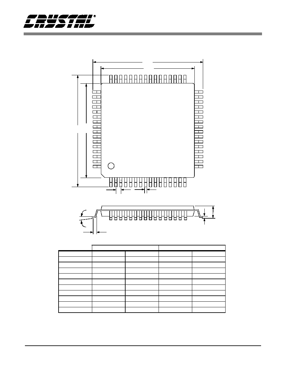
CS7666
40
DS302PP1
PACKAGE DIMENSIONS
INCHES
MILLIMETERS
DIM
MIN
MAX
MIN
MAX
A
0.000
0.063
0.00
1.60
A1
0.002
0.006
0.05
0.15
B
0.007
0.011
0.17
0.27
D
0.461
0.484
11.70
12.30
D1
0.390
0.398
9.90
10.10
E
0.461
0.484
11.70
12.30
E1
0.390
0.398
9.90
10.10
e
0.016
0.024
0.40
0.60
L
0.018
0.030
0.45
0.75
0.000
7.000
0.00
7.00
64L TQFP PACKAGE DRAWING
E1
E
D1
D
1
e
L
B
A1
A

∑ Notes ∑
