 | –≠–ª–µ–∫—Ç—Ä–æ–Ω–Ω—ã–π –∫–æ–º–ø–æ–Ω–µ–Ω—Ç: CS8403 | –°–∫–∞—á–∞—Ç—å:  PDF PDF  ZIP ZIP |

Preliminary Product Information
This document contains information for a new product. Crystal
Semiconductor reserves the right to modify this product without notice.
JAN `97
DS239PP1
1
Copyright
©
Crystal Semiconductor Corporation 1997
(All Rights Reserved)
Crystal Semiconductor Corporation
P.O. Box 17847, Austin, Texas 78760
(512) 445 7222 FAX: (512) 445 7581
http://www.crystal.com
CS8403A CS8404A
96 kHz Digital Audio Transmitter
Features
l
Sample rates up to 108 kHz
l
Supports: AES/EBU, IEC 958, S/PDIF,
& EIAJ CP-340 professional and
consumer formats
l
Generates CRC codes and parity bits
l
On-Chip RS422 line driver
l
Configurable buffer memory (CS8403A)
l
Transparent mode allows direct
connection of CS8404A and CS8414 or
CS8403A and CS8413
l
Pin compatible with CS8401A and
CS8402A
Description
The CS8403A and CS8404A are digital audio transmit-
ters which support 96 kHz sample rate operation. The
devices encode and transmit audio data according to the
AES/EBU, IEC958, S/PDIF, & EIAJ CP-340 interface
standards. The CS8403A and CS8404A accept audio
and digital data, which is then multiplexed, encoded and
driven onto a cable. The audio serial port is double buff-
ered and capable of supporting a wide variety of formats.
The CS8403A has a configurable internal buffer memo-
ry, loaded via a parallel port, which may be used to buffer
channel status, auxiliary data, and/or user data.
The CS8404A multiplexes the channel, user, and validity
data directly from serial input pins with dedicated input
pins for the most important channel status bits.
ORDERING INFO
CS8403A-CS, 0 to 70 ∞C, 24-pin Plastic SOIC
CS8404A-CS, 0 to 70 ∞C, 24-pin Plastic SOIC
I

CS8403A CS8404A
2
DS239PP1
TABLE OF CONTENTS:
GENERAL DESCRIPTION ..................................................................................................... 8
Line Drivers ........................................................................................................................ 8
CS8403A DESCRIPTION ........................................................................................................ 8
Parallel Port ......................................................................................................................... 8
Status and Control Registers ............................................................................................... 8
Serial Port.......................................................................................................................... 11
Buffer Memory.................................................................................................................. 12
Buffer Mode 0 ............................................................................................................. 13
Buffer Mode 1 ............................................................................................................. 14
Buffer Mode 2 ............................................................................................................. 15
Buffer-Read and Interrupt Timing .................................................................................... 15
PIN DESCRIPTIONS ............................................................................................................. 17
Power Supply Connections ......................................................................................... 17
Audio Input Interface .................................................................................................. 17
Parallel Interface ......................................................................................................... 17
Transmitter Interface ................................................................................................... 18
CS8404A DESCRIPTION ...................................................................................................... 19
Audio Serial Port............................................................................................................... 19
C, U, V Serial Port ............................................................................................................ 21
RST and CBL (TRNPT is low)......................................................................................... 21
Transparent Mode ............................................................................................................. 22
Professional Mode............................................................................................................. 23
Consumer Mode ................................................................................................................ 24
Consumer - CD Submode ................................................................................................. 25
PIN DESCRIPTIONS ............................................................................................................. 27
Power Supply Connections ......................................................................................... 27
Audio Input Interface .................................................................................................. 27
Control Pins................................................................................................................. 28
Transmitter Interface ................................................................................................... 29
Appendix A: RS422 Driver Information................................................................................. 30
Appendix B: MCK and FSYNC Relationship ........................................................................ 31

CS8403A CS8404A
DS239PP1
3
ABSOLUTE MAXIMUM RATINGS
(GND = 0V, all voltages with respect to ground.)
Notes: 1. Transient currents of up to 100 mA will not cause SCR latch-up.
WARNING:
Operation at or beyond these limits may result in permanent damage to the device.
Normal operation is not guaranteed at these extremes.
RECOMMENDED OPERATING CONDITIONS
(GND = 0V, all voltages with respect to ground)
Notes: 2. Drivers open (unloaded). The majority of power is used in the load connected to the drivers.
3. Specified to operate over 0 to 70 ∞C but tested at 25 ∞C only.
DIGITAL CHARACTERISTICS
(T
A
= 25 ∞C; VD+ = 5V ±5%)
Notes: 4. MCK for the CS8403A must be 128, 192, 256, or 384x the input word rate based on M0 and M1 in
control register 2. MCK for the CS8404A must be 128x the input word rate, except in Transparent Mode
where MCK is 256x the input word rate.
Specifications are subject to change without notice
Parameters
Symbol
Min
Max
Units
DC Power Supply
VD+
-
6.0
V
Input Current, Any Pin Except Supply
Note 1
I
in
-
±10
mA
Digital Input Voltage
V
IND
-0.3
VD+
V
Ambient Operating Temperature (power applied)
T
A
-55
125
∞C
Storage Temperature
T
stg
-65
150
∞C
Parameters
Symbol Min Typ
Max
Units
DC Voltage
VD+
4.75
5.0
5.25
V
Supply Current
Note 2
I
DD
-
3
10
mA
Ambient Operating Temperature
Note 3
T
A
0
25
70
∞C
Power Consumption
Note 2
P
D
-
15
53
mW
Parameters
Symbol Min Typ
Max
Units
High-Level Input Voltage
V
IH
2.0
-
(VD+) + 0.3
V
Low-Level Input Voltage
V
IL
-0.3
-
+0.8
V
High-Level Output Voltage
I
O
= 200 µA
V
OH
(VD+) - 1.0
-
-
V
Low-Level Output Voltage
I
O
= 3.2 mA
V
OL
-
-
0.4
V
Input Leakage Current
I
in
-
1.0
10
µA
Master Clock Frequency
Note 4
MCK
-
-
27.6
MHz
Master Clock Duty Cycle
40
-
60
%

CS8403A CS8404A
4
DS239PP1
DIGITAL CHARACTERISTICS - RS422 DRIVERS
(TXP, TXN pins only; VD+ = 5.0V ±5%)
SWITCHING CHARACTTERISTICS - CS8403A PARALLEL PORT
(T
A
= 25 ∞C;
VD+ = 5V, Inputs: Logic0 = GND, Logic1 = VD+, C
L
= 20 pF)
Parameters
Symbol Min
Typ
Max
Units
Output High Voltage
I
OH
= -30 mA
V
OH
(VD+) - 0.7
(VD+) - 0.4
-
V
Output Low Voltage
I
OL
= 30 mA
V
OL
-
0.4
0.7
V
Parameters
Symbol Min Typ
Max
Units
ADDRESS valid to CS low
t
adcss
13.5
-
-
ns
CS high to ADDRESS invalid
t
csadh
0
-
-
ns
RD/WR valid to CS low
t
rwcss
10
-
-
ns
CS low to RD/WR invalid
t
csrwi
35
-
-
ns
CS low
t
csl
35
-
-
ns
DATA valid to CS rising
RD/WR low (writing)
t
dcssw
32
-
-
ns
CS high to DATA invalid
RD/WR low (writing)
t
csdhw
0
-
-
ns
CS falling to DATA valid
RD/WR high (reading)
t
csddr
-
-
35
ns
CS rising to DATA Hi-Z
RD/WR high (reading)
t
csdhr
5
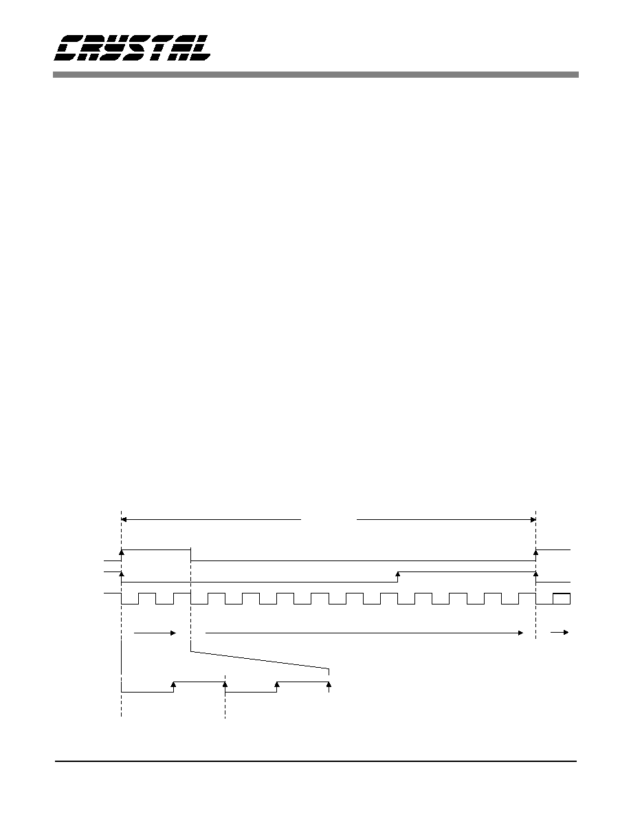
-
-
ns
A4 - A0
D7 - D0
RD/WR
Writing
Reading
adcss
t
csddr
t
csl
t
dcssw
t
csdhw
t
csdhr
t
csadh
t
CS
D7 - D0
RD/WR
csrwi
t
rwcss
t
CS8403A Parallel Port Timing

CS8403A CS8404A
DS239PP1
5
SWITCHING CHARACTERISTICS - SERIAL PORTS
(T
A
= 25 ∞C; VD+ = 5V; Inputs: Logic0 = GND, Logic1 = VD+; C
L
= 20 pF)
Notes: 5. The input word rate (IWR) refers to the frequency at which stereo audio input sample pairs are input to
the part. (A stereo pair is two audio samples.) Therefore, in Master mode, there are always 32 SCK
periods in one audio sample.
6. Master mode is defined as SCK and FSYNC being outputs. In Slave mode they are inputs. In the
CS8403A, control register 3 bit 1, MSTR, selects master. In the CS8404A, only format 0 is master.
7. The table above assumes data is output on the falling edge and latched on the rising edge. In both parts
the edge is selectable. The table is defined for the CS8403A with control register 3 bit 0, SCED, set to
one, and for the CS8404A in formats 4 through 7. For the other formats, the table and figure edges must
be reversed (i.e. "rising" to "falling" and vice versa).
8. The diagrams show SBC rising coincident with the first rising edge of SCK after FSYNC transitions.
This is true for all modes except FSF0 & 1 both equal 1 in the CS8403A, and format 4 in the CS8404A.
In these modes SBC is delayed one full SCK period.
Parameters
Symbol Min Typ
Max
Units
Input Word Rate
Note 5
IWR
-
-
108
kHz
SCK Frequency
Master Mode
Note 6
Slave Mode
Note 6
t
sckf
-
-
IWR x 64
-
12.5
Hz
MHz
SCK Pulse Width Low
Slave Mode
Note 6
t
sckl
25
-
-
ns
SCK Pulse Width High
Slave Mode
Note 6
t
sckh
25
-
-
ns
SCK rising to FSYNC edge delay
Notes 6, 7
t
sfds
20
-
-
ns
SCK rising to FSYNC edge setup
Notes 6, 7
t
sfs
20
-
-
ns
SDATA valid to SCK rising setup
Note 7
t
sss
20
-
-
ns
SCK rising to SDATA hold time
Note 7
t
ssh
20
-
-
ns
C, U, V valid to SCK rising setup
CS8404A
non-CD Mode Notes 7, 8
t
css
0
-
-
ns
SCK rising to C, U, V hold time
CS8404A
non-CD Mode Notes 7, 8
t
scs
50
-
-
ns
U valid to SBC rising setup
Note 8
CS8404A, CD mode
t
uss
0
-
-
ns
SBC rising to U hold time
Note 8
CS8404A, CD mode
t
suh
80
-
-
ns
RST Pulse Width
CS8404A
150
-
-
ns
sckh
t
sfs
t
sfds
t
sss
t
ssh
t
sckl
t
SDATA
SCK
FSYNC
Serial Input Timing - Slave Mode

CS8403A CS8404A
6
DS239PP1
sckf
t
sfs
t
sss
t
SDATA
SCK
FSYNC
ssh
t
css
t
C,U,V
CS8404A
suh
t
U
SBC
uss
t
sch
t
non-CD mode
CD mode
sfds
t
Serial Input Timing - Master Mode & C, U, V Port
External
Clock
Transmitter
Circuit
See Appendix B
+5V
5k
7
6
8
15
14
16
FSYNC
SCK
SDATA
INT
CS
RD/WR
A0-A4
D0-D7
MCK
5
VD+
GND
TXP
TXN
19
18
20
17
+5V
0.1 µF
CS8403A
Audio
Data
Processor
Audio
Data
Processor
or
Microcontroller
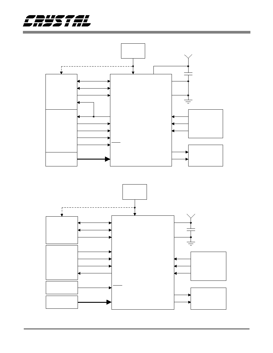
Figure 1. CS8403A Typical Connection Diagram
CS8403A CS8404A
DS239PP1
7
External
Clock
Transmitter
Circuit
See Appendix B
7
6
8
15
10
11
FSYNC
SCK
SDATA
CBL
C
U
V
RST
MCK
5
GND
TRNPT
TXP
TXN
18
24
20
17
0.1 µF
CS8404A
Microcontroller
or
unused
Channel Status
Bits Control
Audio
Data
Processor
8 Dedicated C.S. Bits
+5V
VD+
19
9
16
M2
M1
23
22
M0
21
Serial Port
Mode Select
Figure 2. CS8404A Professional & Consumer Modes Typical Connection Diagram
External
Clock
Transmitter
Circuit
See Appendix B
7
6
8
9
10
11
FSYNC
SCK
SDATA
V
SBF
U
SBC
RST
MCK
5
GND
TXP
TXN
19
18
20
17
0.1 µF
CS8404A
Decoder
Subcode
Port
Channel Status
Bits Control
Audio
Data
Processor
8 Dedicated C.S. Bits
+5V
VD+
15
16
M2
M1
23
22
M0
21
Serial Port
Mode Select
Reset
Control
Figure 3. Consumer CD Submode Typical Connection Diagram

CS8403A CS8404A
8
DS239PP1
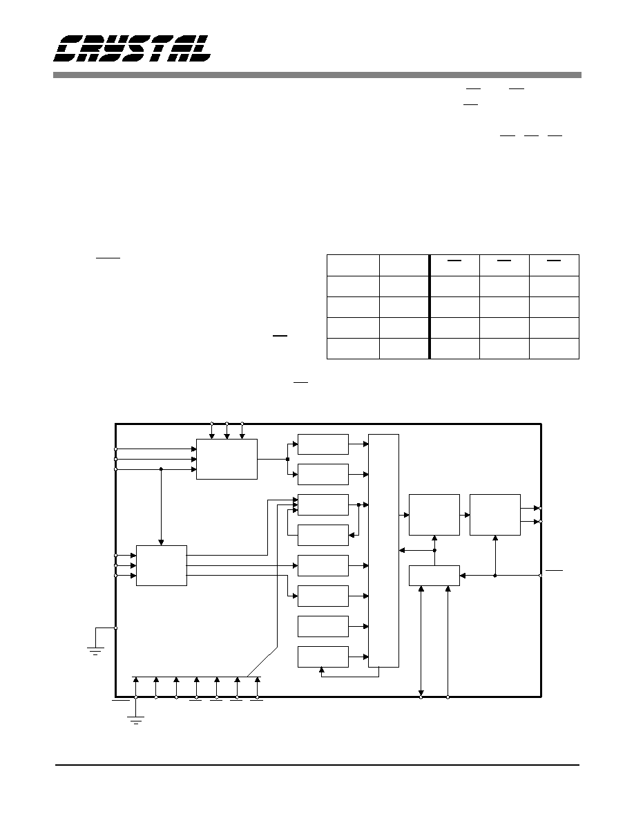
GENERAL DESCRIPTION
The CS8403A/4A are monolithic CMOS circuits
that encode and transmit audio and digital data ac-
cording to the AES/EBU, IEC958 (S/PDIF), and
EIAJ CP-340 interface standards. Both chips ac-
cept audio and control data separately, multiplex
and biphase-mark encode the data internally, and
drive it, directly or through a transformer, to a
transmission line. The CS8403A is fully software
programmable through a parallel port and contains
buffer memory for control data, while the
CS8404A has dedicated pins for the most impor-
tant control bits and a serial input port for the C, U,
and V bits.
Familiarity with the AES/EBU and IEC958 speci-
fications are assumed throughout this data sheet.
Many terms such as channel status, user data, aux-
iliary data, professional mode, etc. are not defined.
The Application Note, Overview of AES/EBU
Digital Audio Interface Data Structures, provides
an overview of the AES/EBU and IEC958 specifi-
cations and is included for clarity; however, it is not
meant to be a complete reference, and the complete
standards should be obtained from the Audio Engi-
neering Society or ANSI for the AES/EBU docu-
ment, and the International Electrotechnical
Commission for the IEC document.
Line Drivers
The RS422 line drivers for both the CS8403A and
CS8404A are low skew, low impedance, differen-
tial outputs capable of driving 110
transmission
lines with a 4 Vpp signal when configured as
shown in Appendix A. To prevent possible short
circuits, both drivers are set to ground when no
master clock (MCK) is provided. They can also be
disabled by resetting the device (RST = low). Ap-
pendix A contains more information on the line
drivers. A 0.1 µF capacitor, with short leads, should
be placed as close as possible to the VD+ and GND
pins.
CS8403A DESCRIPTION
The CS8403A accepts 16- to 24-bit audio samples
through a configurable serial port, and channel sta-
tus, user, and auxiliary data through an 8-bit paral-
lel port. The parallel port allows access to 32 bytes
of internal memory which is used to store control
information and buffer channel status, user, and
auxiliary data. This data is multiplexed with the au-
dio data from the serial port, the parity bit is gener-
ated, and the bit stream is biphase-mark encoded
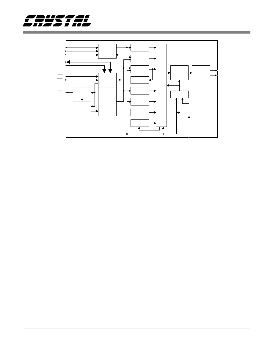
and driven through an RS422 line driver. A block
diagram of the CS8403A is shown in Figure 4. In
accordance with the professional definition of
channel status, the CRCC code (C.S. byte 23) can
be internally generated.
Parallel Port
The parallel port accesses one status register, three
control registers, and 28 bytes of dual port buffer
memory. The address bus and RD/WR line must be
valid when CS goes low. If RD/WR is low, the val-
ue on the data bus will be written into the buffer
memory at the specified address. If RD/WR is high,
the value in the buffer memory, at the specified ad-
dress, is placed on the data bus. The detailed timing
for reading and writing the CS8403A can be found
in the Digital Switching Characteristics table. The
memory space is allocated as shown in Figure 5.
There are three defined buffer memory modes se-
lectable by two bits in control register 2.
Status and Control Registers
Upon power up the CS8403A control registers con-
tain all zeros. Therefore, the part is initially in reset
and is muted. One's must be written to control reg-
ister 2, bits RST and MUTE, before the part will
transmit data. The remaining registers are not ini-
tialized on power-up and may contain random da-
ta.
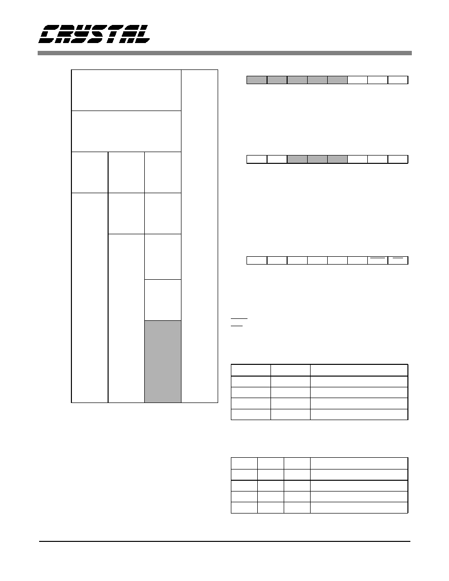
The first register, shown in Figure 6, is the status
register in which only three bits are valid. The low-
er three bits contain flags indicating the position of
CS8403A CS8404A
DS239PP1
9
the transmit pointer in the buffer memory. These
flags may be used to avoid contention between the
transmit pointer reading the data and the user up-
dating the buffer memory. Besides indicating the
byte location being transmitted, the flags indicate
the block of memory the part is currently address-
ing, thereby telling the user which block is free to
be written. Each flag has a corresponding mask bit
(control register1) which, when set, allows a transi-
tion on the flag to generate a pulse on the interrupt
pin. Flag 0 and flag 1 cause interrupts on both edges
whereas flag 2 causes an interrupt only on the ris-
ing edge. Timing and further explanation of the
flags can be found in the buffer memory section.
The two most significant bits of control register 1,
BKST and TRNPT, are used for Transparent Mode
operation of the CS8403A. Transparent Mode is
used for those applications where it is useful to
maintain frame alignment between the received
and transmitted audio data signals. In Transparent
Mode (TRNPT="1") the MCK, FSYNC, SCK and
SDATA inputs of the CS8403A can be connected
to their corresponding outputs of the CS8413. In
Transparent Mode, FSYNC synchronizes the trans-
mitter and the receiver. The data delay through the
CS8403A is set so that three frame delays occur
from the input of the CS8413 to the output of the
CS8403A. In Transparent Mode, 32 SCKs are re-
quired per subframe.
Channel status block alignment between the
CS8413 and the CS8403A is accomplished by set-
ting BKST high at the occurrence of the Flag 2 ris-
ing edge of the CS8413. If FSYNC is a left/right
signal, BKST is sampled once per frame; if
FSYNC is a word clock, BKST is sampled once per
subframe. A low to high transition of BKST (based
on two successive internal samples) resets the
channel status block boundary to the beginning.
Control register 2, shown in Figure 8, contains var-
ious system level functions. The two most signifi-
cant bits, M1 and M0, select the frequency at the
MCK pin as shown in Table 1. As an example, if
the audio sample frequency is 44.1 kHz and M0
and M1 are both zero, MCK would then be 128x
the audio sample rate or 5.6448 MHz. The next bit
(5) in control register 2, V, indicates the validity of
the current audio sample. According to the digital
audio specifications, V=0 signifies that the audio
signal is suitable for conversion to analog. B1 and
SDATA
SCK
FSYNC
D[0:7]
A[0:3]
CS
RD/WR
INT
8
6
7
1-4,21-24
9-13
14
16
15
Serial
Port
Logic
Interrupt
Control
Read
Address
Generator
Control
and Flags
4 X 8
Buffer
Memory
28 X 8
Audio
Aux
C Bits
CRC
U Bits
Validity
Preamble
Parity
Mux
Biphase
Mark
Encoder
Timing
IMCK
Prescaler
5
MCK
Line
Driver
20
17
TXP
TXN
Figure 4. CS8403A Block Diagram
CS8403A CS8404A
10
DS239PP1
B0 select one of three modes for the buffer memo-
ry. The different modes are shown in Figure 5 and
the bit combinations in Table 2. More information
on the different modes can be found in the Buffer
Memory section. Bit 2, CRCE, is the channel sta-
tus CRCC enable and should only be used in pro-
fessional mode. When CRCE is high, the channel
status data cyclic redundancy check characters are
A
D
D
R
E
S
S
0
Status register 0
Control Register 1
Control Register 2
Control Register 3
U
N
D
E
F
I
N
E
D
1
2
3
4
User Data
5
6
7
8
1st Four
Bytes of
C.S. Data
1st Four
Bytes of
C.S. Data
1st Four
Bytes of
Left C. S.
Data
9
A
B
C
Last 20
Bytes
Channel
Status
Data
C. S.
Data
Left C. S.
Data
D
E
F
10
Auxiliary
Data
1st Four
Bytes of
Right
C. S.
Data
11
12
13
14
Right
C. S.
Data
15
16
17
18
19
1A
1B
1C
1D
1E
1F
0
1
2
3
Memory Mode
Figure 5. CS8403A Buffer Memory Modes
FLAG2:
High for first four bytes of channel status
FLAG1:
Memory mode dependent - See Figure 11
FLAG0:
High for last two bytes of user data
Figure 6. Status Register
BKST:
Causes realignment of data block when set to "1"
TRNPT: Selects Transparent Mode appropriatley setting data delay
through device
MASK2: Interrupt mask for FLAG2. A "1" enables the interrupt.
MASK1: Interrupt mask for FLAG1.
MASK0: Interrupt mask for FLAG0.
Figure 7. Control Register 1
M1:
with M0, selects MCK frequency.
M0:
with M1, selects MCK frequency.
V:
Validity bit of current sample.
B1:
with B0, selects the buffer memory mode
B0:
with B1, selects the buffer memory mode
CRCE:
Channel status CRC Enable. Professional mode only.
MUTE:
When clear, transmitted audio data is set to zero.
RST:
When clear, drivers are disabled, frame counters cleared.
Figure 8. Control Register 2
Table 1. MCLK Frequencies
Table 2. Buffer Memory Modes
7
6
5
4
3
2
1
0
X:00
FLAG2 FLAG1 FLAG0
7
6
5
4
3
2
1
0
X:01
BKST
TRNPT
MASK2 MASK1 MASK0
7
6
5
4
3
2
1
0
X:02
M1
M0
V
B1
B0
CRCE
MUTE
RST
M1
M0
MCLK
0
0
128x Input Word Rate
0
1
192x Input Word Rate
1
0
256x Input Word Rate
1
1
384x Input Word Rate
B1
B0
Mode
Buffer Memory Contents
0
0
0
Channel Status
0
1
1
Auxiliary Data
1
0
2
Independent Channel Status
1
1
3
Reserved

CS8403A CS8404A
DS239PP1
11
generated independently for channels A and B and
are transmitted at the end of the channel status
block. When MUTE (bit 1) is low, the transmitted
audio data is forced to zero. Both RST and MUTE
are set to zero upon power up.
When RST is low, the differential line drivers are
set to ground and the block counters are reset to the
beginning of the first block. In order to properly
synchronize the rest of the CS8403A to the audio
serial port, the transmit timing counters, which in-
clude the flags in the status register, are not enabled
after RST is set high until eight and one half SCK
periods after the active edge (first edge after reset is
exited) of FSYNC.
When FSYNC is configured as a left/right signal
(FSF1=1), the counters and flags are not enabled
until the right sample is being entered (during
which the previous left sample is being transmit-
ted). This guarantees that channel A is left and
channel B is right as per the digital audio interface
specs.
Control register 3 contains format information for
the serial audio input channel. The MSB is unused
and the next three bits, SDF2-SDF0, select the for-
mat for the serial input data with respect to
FSYNC. There are five valid combinations of these
bits as shown in Figure 10. The next two bits, FSF1
and FSF0, select the format of FSYNC. Two of the
formats delineate each channel's data and do not in-
dicate the particular channel. The other two formats
also indicate the specific channel. The formats are
shown in Figure 10. Bit1, MSTR, determines
whether FSYNC and SCK are inputs, MSTR low,
or outputs, MSTR high. Bit0, serial clock edge se-
lect, SCED, selects the edge that audio data gets
latched on. When SCED is low, the falling edge of
SCK latches data in the chip and when SCED is
high, the rising edge is used.
SDF2:
with SDF0 & SDF1, select serial data format.
SDF1:
with SDF0 & SDF2, select serial data format.
SDF0:
with SDF1 & SDF2, select serial data format.
FSF1:
with FSF0, select FSYNC format.
FSF0:
with FSF1, select FSYNC format.
MSTR:
When set, SCK and FSYNC are outputs.
SCED:
When set, rising edge of SCK latches data.
When clear, falling edge of SCK latches data.
Figure 9. Control Register 3
The multitude of combinations allow for a zero
glue logic interface to almost all DSPs, encoder
chips, and standard serial data formats.
Serial Port
The serial port is used to enter audio data and con-
sists of three pins: SCK, SDATA, and FSYNC. The
serial port is double buffered with SCK clocking in
the data from SDATA, and FSYNC delineating au-
dio samples and may define the particular channel,
left or right.
Control register 3, shown in Figure 9, configures
the serial port. All the various formats are illustrat-
ed in Figure 10. When FSF1 is low, FSYNC only
delineates audio samples. When FSF1 is high, it de-
lineates audio samples and specifies the channel.
When FSF1 is low and the port is a master (MSTR
= 1), FSYNC is a square wave output. When FSF1
is low and the port is a slave (input), FSYNC can be
a square wave or a pulse provided the active edge,
as defined in Figure 10, is properly positioned with
respect to SDATA.
Bits 4, 5, and 6, SDF0-SDF2, define the format of
SDATA and is also described in Figure 10. The
five allowable formats are MSB first, MSB last, 16-
bit LSB last, 18-bit LSB last, and 20-bit LSB last.
The MSB first and MSB last formats accept any
word length from 16 to 24 bits. The word length is
controlled by providing trailing zeros in MSB first
mode and leading zeros in MSB last mode, or by re-
stricting the number of SCK periods between sam-
ples to the sample word length. The 16-, 18-, and
20-bit LSB-last modes require at least 16, 18, or 20
7
6
5
4
3
2
1
0
X:03
SDF2
SDF1
SDF0
FSF1
FSF0
MSTR
SCED

CS8403A CS8404A
12
DS239PP1
SCK periods per sample respectively. As a master,
32 SCK periods are output per sample.
FSYNC must be derived from MCK via a DSP us-
ing the same clock or by external counters. If
FSYNC moves (jitters) with respect to MCK by
more than 4 MCK periods, the CS8403A may reset
the channel status block and flags. Appendix C
contains more information on the relationship of
FSYNC and MCK.
Buffer Memory
In all buffer modes, the status register and control
registers are located at addresses 0-3 respectively,
and the user data is buffered in locations 4-7. The
parallel port can access any location in the user data
buffer at any time; however, care must be taken not
to modify a location when that location is being
read internally. This internal reading is done
through the second port of the buffer in a cyclic
manner.
Reset initializes the internal pointer to 04H(Hex).
Data is read from this location and stored in an 8-
bit shift register which is shifted once per audio
sample. (An audio sample is defined as a single
channel, not a stereo pair.) The byte is transmitted
LSB first, D0 being the first bit. After transmitting
8 samples, i.e. 8 user bits, the address pointer is in-
cremented and the next byte of user data is loaded
into the shift register. After transmitting all four
bytes, 32 audio samples, the user read pointer is re-
set to 04H (Hex) and the cycle repeats.
Flag 0 in the status register monitors the position of
the internal user data read pointer. When the first
byte, location 04H, is read, flag 0 is set low and
when the third byte, location 06H, is read, flag 0 is
set high. If mask 0 in control register1 is set, a tran-
sition of flag 0 will generate a low pulse on the in-
terrupt pin. The value of flag 0 indicates which two
bytes the part will read next, thereby indicating
which two bytes are free to be updated.
Flag 1 is mode dependent, changing with buffer
memory configuration, and is discussed in the indi-
vidual buffer mode sections.
210 (bit)
000
001
010
100
110
FSF
00
01
10
11
00
01
10
11
MSTR
0
0
0
0
1
1
1
1
MSB First
MSB Last
LSB Last 16
LSB Last 18
LSB Last 20
FSYNC Input
FSYNC Input
FSYNC Input
FSYNC Input
FSYNC Output
FSYNC Output
FSYNC Output
FSYNC Output
Name
LSB
MSB
LSB
MSB
LSB
LSB
LSB
MSB
LSB
MSB
LSB
LSB
MSB
LSB
MSB
MSB
LSB
MSB
LSB
MSB
MSB
LSB
MSB
LSB
MSB
16 Bits
18 Bits
20 Bits
18 Bits
16 Bits
Left Sample
Right Sample
20 Bits
16 Clocks
16 Clocks
16 Clocks
16 Clocks
32 Clocks
32 Clocks
32 Clocks
32 Clocks
10 (bit)
SDF
24 bits, incl. Aux
24 bits, incl. Aux
24 bits, incl. Aux
24 bits, incl. Aux
Figure 10. CS8403A Serial Port SDATA and FSYNC Timing

CS8403A CS8404A
DS239PP1
13
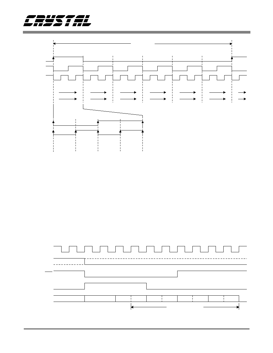
Flag 2 is set high when byte 0 of the channel status,
address 08H, is read, and set low when byte 4, ad-
dress 0BH, is read. Therefore, flag 2 high indicates
the part is reading the first four bytes of channel
status and the last 20 bytes are free to update. If the
interrupt mask bit for flag 2 is set, the rising edge
will cause an interrupt indicating the beginning of
a channel status block as shown in Figure 11. Al-
though a falling edge on flag 0 and flag 1 may cause
an interrupt, the falling edge of flag 2 will not.
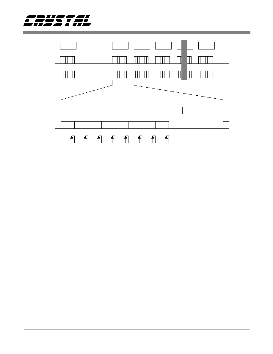
Figure 11 illustrates the flag timing for an entire
channel status block which includes 24 bytes of
channel status data and 384 audio samples. (This
figure assumes the channel status bit is the same for
the audio pair.) The lower portion of Figure 11 ex-
pands the first byte of channel status showing eight
pairs of data with a pair defined as a frame. This is
further expanded showing the first sub-frame (A0)
to contain 32 bits as per the AES/EBU specifica-
tions (see Appendix A). When transmitting stereo,
channel A is left and channel B is right. The pream-
ble at the bottom of Figure 11 is expanded in
Figure 15 to show the exact timing between flags,
the interrupt pin, and internal buffer-read timing.
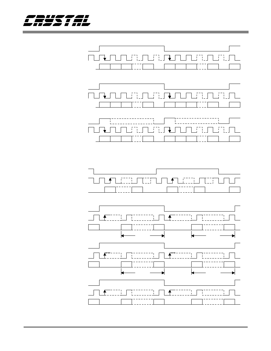
Buffer Mode 0
In buffer mode 0, in addition to the user-data buffer
previously discussed, one entire block of channel
status data is buffered in 24 memory locations from
address 08H to 1FH. This block will be transmitted
Flag 0
Flag 1
Mode 0
Flag 1
Modes 1 & 2
Flag 2
0
3 4
7
8
Audio Data
28 29 30 31
27
23 0
1
2
3
4
5
6
7
8
9 10 11 12 13 14 15 16 17 18 19 20 21 22 23 0
1
Channel Status Byte
(Expanded)
(Expanded)
bit
Frame
Sub-frame
Block
(384 Audio Samples)
See figure 15
Validity
User Data
Channel Status Data
Parity Bit
V U C P
MSB
Aux Data
LSB
Preamble
B 0
A 0
A 1
B 1
B 2
A 2
B 7
A 7
Figure 11. CS8403A Status Register Flag Timing
CS8403A CS8404A
14
DS239PP1
in both channel A and channel B, one bit per frame.
Like the user-data buffer, the parallel port can ac-
cess any location in this buffer at any time. The
transmitter section reads this buffer in a cyclic non-
destructive manner and stores the byte in an 8-bit
shift register that is shifted once per two transmit-
ted audio samples (once per frame).
Flag1 in the status register can be used to monitor
the channel status buffer. In mode 0, flag 1 is set
low when byte 0, location 08H, is read and set high
when byte 16, location 18H, is read. If mask 1 in
control register 1 is set, a transition on flag 1 will
generate a pulse on the interrupt pin. Figure 12 il-
lustrates the memory read sequence for buffer
mode 0 along with the flag timing. The arrows on
the flags indicate an interrupt if the appropriate
mask bit is set. Flag 0 can cause an interrupt on ei-
ther edge, which is shown only in the expanded
portion of the Figure for clarity. The expanded sec-
tion also shows that the user buffer is reread when
location 0AH of the channel status is read.
Buffer Mode 1
In buffer mode 1, eight bytes are allocated for chan-
nel status data and 16 bytes for auxiliary data as
shown in Figure 5. The channel status buffer, loca-
tions 08H to 0FH, is divided into two sections. The
first four locations always contain the first four
bytes of channel status, identical to mode 0, and are
read once per channel status block. The second four
locations, addresses 0CH to 0FH, provide a cyclic
buffer for the last 20 bytes of channel status data.
Similar to mode 0, transmitted channel status data
will be the same for channel A and channel B (one
channel status bit per frame). Flag 1 and flag 2 can
be used to monitor this buffer. Flag 1 is set low
when byte 0 of channel status data, location 08H, is
read and is toggled when every other byte is read.
As shown in Figure 13, flag 2 is set high when byte
0, location 08H, is read and set low when byte 4, lo-
cation 0CH, is read. Flag 2 determines whether the
channel status pointer is reading the first four-byte
section or the second four-byte section, while flag
1 indicates which two bytes of the section are free
to update.
The auxiliary data buffer, locations 10H to 1FH, is
read in a cyclic manner similar to the data buffer;
however, four auxiliary data bits are transmitted
per audio sample (sub-frame). Since the auxiliary
buffer must be read four times as often as the user
data buffer and is four times as large, flag 0 can be
used to monitor both.
Flag 0
Flag 1
Flag 2
(Expanded)
Block
(384 Audio Samples)
08
0B
1F
C.S. Address
0
1
2
3
4
5
6
7
8
9
10
11
12
13
14
15
16
17
18
19
20
21
22
23
0
1
C.S. Byte
Flag 0
08
09
0A
0B
04
05
06
07
04
05
06
07
C.S. Address
User Address
(Addresses are in Hex)
0C
08
Figure 12. CS8403A Buffer Momory Read Sequence - MODE 0

CS8403A CS8404A
DS239PP1
15
Buffer Mode 2
In buffer mode 2, two 8-byte buffers are available
for buffering both channel A and channel B chan-
nel status data independently. Both buffers are
identical to the channel status buffer in mode 1 ex-
cept that each channel can have unique channel sta-
tus data. The two buffers are read simultaneously
with locations 08H to 0FH transmitted in channel A
and locations 10H to 17H transmitted in channel B.
Figure 5 contains the buffer memory modes and
Figure 14 illustrates the buffer read sequence for
mode 2.
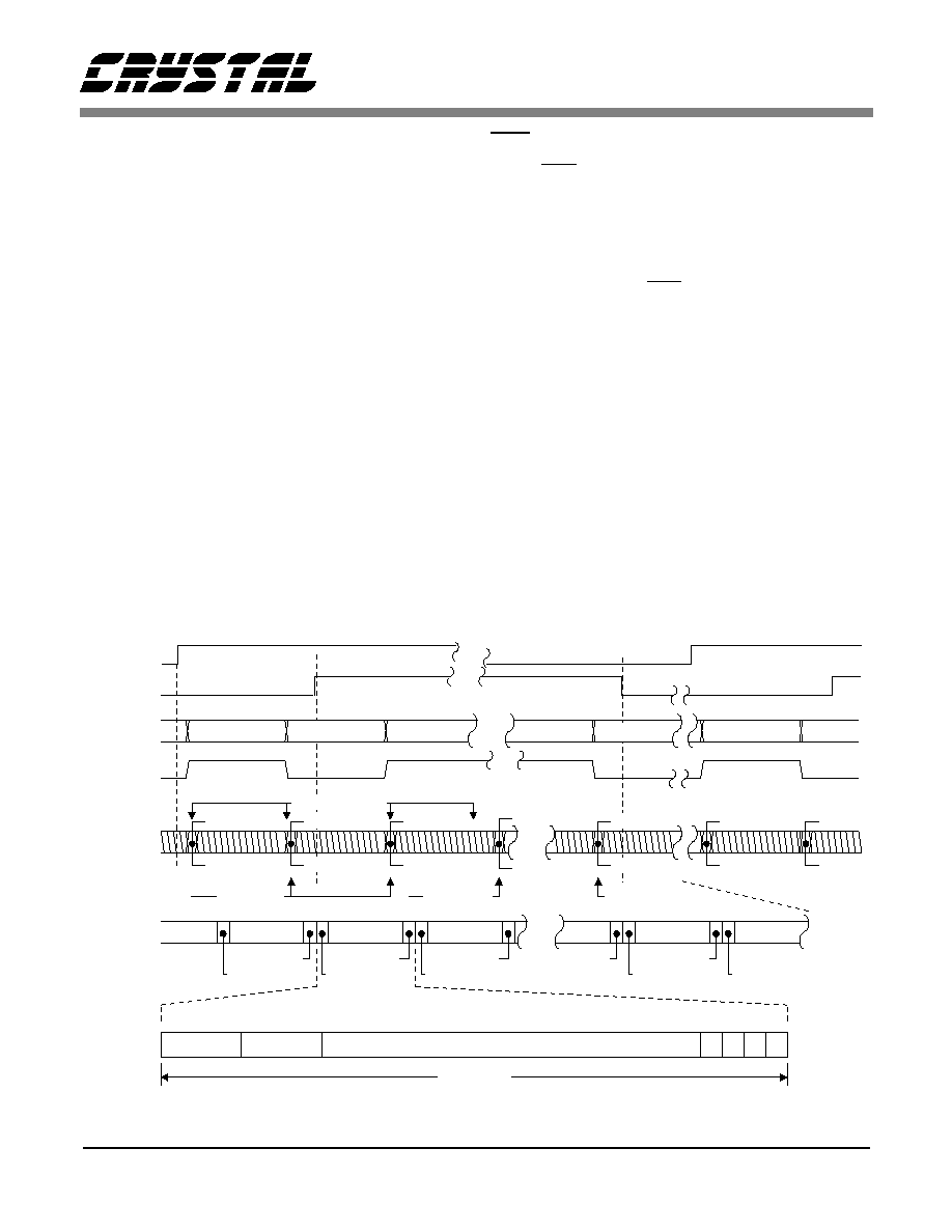
Buffer-Read and Interrupt Timing
As mentioned previously in the buffer mode sec-
tions, conflicts between externally writing to the
buffer ram and the CS8403A internally reading
bytes of ram for transmission may be averted by us-
ing the flag levels to avoid the section currently be-
ing addressed by the part. Interrupts occur at flag
edges indicating the exact byte that the part is cur-
rently reading. Utilizing INT along with the flags,
the byte currently being read by the part can be
avoided allowing access to all other bytes instead
of just a section. Figure 15 illustrates the timing be-
tween flags, INT, and the internal reading of the
buffer for transmission. The master clock IMCK is
shown as 128x Fs. Other MCK frequencies are ini-
tially divided to obtain 128x Fs, defined as IMCK
(internal MCK), which is then used for all internal
timing, so the timing in Figure 15 is valid for all
MCK frequencies. When the parity bit (P) is trans-
mitted, a transition on a flag causes INT to go low
if the appropriate mask bit is set. Concurrently, the
part starts reading from the internal buffer. Writing
to the buffer ram location being read by the part
should be avoided while the internal "ram read"
signal is high.
Flag 0
Flag 1
Flag 2
(Expanded)
Block
(384 Audio Samples)
08
0B 0C
0F 08
C.S. Address
0
1
2
3
4
5
6
7
8
9
10
11
12
13
14
15
16
17
18
19
20
21
22
23
0
1
C.S. Byte
Flag 0
08
09
0A
0B
04
05
06
07
04
05
06
07
C.S. Address
User Address
(Addresses are in Hex)
0F 0C
0F 0C
0F 0C
0F 0C
10
13,14
17 18
1B,1C
1F 10
13,14
17 18
1B,1C
1F
Flag 1
Aux. Address
Figure 13. CS8403A Buffer Memory Read Sequence - MODE 1
CS8403A CS8404A
16
DS239PP1
Flag 0
Flag 1
Flag 2
Block
(384 Audio Samples)
Left C.S. Ad.
0
1
2
3
4
5
6
7
8
9
10
11
12
13
14
15
16
17
18
19
20
21
22
23
0
1
C.S. Byte
(Addresses are in Hex)
(Expanded)
Flag 0
08
09
0A
0B
05
06
07
04
05
06
07
Left C.S. Ad.
User Address
08
0B 0C
0F 08
0F 0C
0F 0C
0F 0C
0F 0C
10
13 14
14 10
17 14
17 14
17 14
17 14
Right C.S. Ad.
04
10
11
12
13
Right C.S. Ad.
Flag 1
Figure 14. CS8403A Buffer Memory Read Sequence - MODE 2
IMCK (128Fs)
Flags 0 & 1
Flag 2
INT
RAM Read
TXP
TXN
C
P
Transmit Preamble
Figure 15. RAM/Buffer-Read and Interrupt Timing

CS8403A CS8404A
DS239PP1
17
PIN DESCRIPTIONS
Power Supply Connections
VD+ - Positive Digital Power, PIN 19.
Positive supply for the digital section. Nominally +5 volts.
GND - Ground, PIN 18.
Ground for the digital section.
Audio Input Interface
SCK - Serial Clock, PIN 6.
Serial clock for SDATA pin which can be configured (via control register 3) as an input or
output, and can sample data on the rising or falling edge. As an output, SCK will contain 32
clocks for every audio sample. As an input, it does not need to be continuous and can be up to
15 MHz.
FSYNC - Frame Sync, PIN 7.
Delineates the serial data and may indicate the particular channel, left or right. Also, FSYNC
may be configured as an input or output. The format is based on bits in control register 3.
SDATA - Serial Data, PIN 8.
Audio data serial input pin.
Parallel Interface
CS - Chip Select, PIN 14.
This input is active low and allows access to the 32 bytes of internal memory. The address bus
and RD/WR must be valid while CS is low.
1
2
3
4
5
6
7
8
9
10
11
12
24
23
22
21
20
19
18
17
16
15
14
13
D4
D5
D6
D7
MCK
SCK
FSYNC
SDATA
A4
A3
A2
A1
DATA BUS BIT 4
DATA BUS BIT 5
DATA BUS BIT 6
DATA BUS BIT 7
MASTER CLOCK
SERIAL DATA CLOCK
FRAME SYNC
SERIAL INPUT DATA
ADDRESS BUS BIT 4
ADDRESS BUS BIT 3
ADDRESS BUS BIT 2
ADDRESS BUS BIT 1
D3
D2
D1
D0
TXP
VD+
GND
TXN
RD/WR
INT
CS
A0
DATA BUS BIT 3
DATA BUS BIT 2
DATA BUS BIT 1
DATA BUS BIT 0
TRANSMIT POSITIVE
POWER
GROUND
TRANSMIT NEGATIVE
READ/WRITE SELECT
INTERRUPT
CHIP SELECT
ADDRESS BUS BIT 0
CS8403A

CS8403A CS8404A
18
DS239PP1
RD/WR - Read/Write, PIN 16.
If RD/WR is low when CS goes active (low), the data on the data bus is written to internal
memory. If RD/WR is high when CS goes active, the data in the internal memory is placed on
the data bus.
A4-A0 - Address Bus, PINS 9-13.
Parallel port address bus that selects the internal memory location to be read from or written to.
D0-D7 - Data Bus, PINS 21-24, 1-4.
Parallel port data bus used to check status, write control words, or write internal buffer
memory.
INT - Interrupt, PIN 15.
Open drain output that can signal the state of the internal buffer memory. A 5 k
resistor to
VD+ is typically used to support logic gates. All bits affecting INT are maskable allowing total
control over the interrupt mechanism.
Transmitter Interface
MCK - Master Clock, PIN 5.
Clock input which defines the transmit timing. It can be configured, via control register 2, for
128, 192, 256, or 384 times the sample rate.
TXP, TXN - Differential Line Drivers, PINS 20, 17.
RS422 compatible line drivers. Drivers are pulled low when part is in reset state.
CS8403A CS8404A
DS239PP1
19
CS8404A DESCRIPTION
The CS8404A accepts 16- to 24-bit audio samples
through a serial port configured in one of seven for-
mats, provides several pins dedicated to particular
channel status bits, and allows all channel status,
user, and validity bits to be serially input through
port pins. This data is multiplexed, the parity bit is
generated, and the bit stream is biphase-mark en-
coded and driven through an RS422 line driver.
The CS8404A operates as a professional or con-
sumer interface transmitter selectable by pin 2,
PRO. As a professional interface device, the dedi-
cated channel status input pins are defined accord-
ing to the professional standard, and the CRC code
(C.S. byte 23) can be internally generated.
As a consumer device, the dedicated channel status
input pins are defined according to the consumer
standard. A submode provided under the consumer
mode is compact disk, CD, mode. When transmit-
ting data from a compact disk, the CD subcode port
can accept CD subcode data, extract channel status
information from it, and transmit it as user data.
The master clock, MCK, controls timing for the en-
tire chip and must be 128x Fs. As an example, if
stereo data is input to the CS8404A at 44.1 kHz,
MCK input must be 128 times that or 5.6448 MHz.
Audio Serial Port
The audio serial port is used to enter audio data and
consist of three pins: SCK, SDATA, and FSYNC.
SCK clocks in SDATA, which is double buffered,
while FSYNC delineates the audio samples and
may indicate the particular channel, left or right. To
support many different interfaces, M2, M1, and M0
select one of seven different formats for the serial
port. The coding is shown in Table 3 while the for-
mats are shown in Figure 16. Format 0 and 1 are de-
signed to interface with Crystal ADCs. Format 2
communicates with Motorola and TI DSPs.
Format 3 is reserved. Format 4 is compatible with
the I
2
S standard. Formats 5 and 6 make the
CS8404A look similar to existing 16- and 18-bit
DACs, and interpolation filters. Format 7 is an
MSB-last format and is conducive to serial arith-
metic. SCK and FSYNC are outputs in Format 0
and inputs in all other formats. In Format 2, the ris-
ing edge of FSYNC delineates samples and the fall-
ing edge must occur a minimum of one bit period
before or after the rising edge. In all formats
except 2, FSYNC contains left/right information
requiring both edges of FSYNC to delineate sam-
ples. Formats 5 and 6 require a minimum of 16- or
18-bit audio words respectively. In all formats oth-
er than 5 and 6, the CS8404A can accept any word
length from 16 to 24 bits by adding leading zeros in
format 7 and trailing zeros in the other formats, or
by restricting the number of SCK periods between
active edges of FSYNC to the sample word length.
Table 3. CS8404A Audio Port Modes
FSYNC must be derived from MCK, either through
a DSP using the same clock, or using counters. If
FSYNC moves (jitters) with respect to MCK by
four MCK periods, the internal counters and CBL
may be reset. Appendix B contains more informa-
tion on the relationship between FSYNC and
MCK.
M2
M1
M0
Format
0
0
0
0 - FSYNC & SCK Output
0
0
1
1 - Left/Right, 16-24 Bits
0
1
0
2 - Word Sync, 16-24 Bits
0
1
1
3 - Reserved
1
0
0
4 - Left/Right, I
2
S Compatible
1
0
1
5 - LSB Justified, 16 Bits
1
1
0
6 - LSB Justified, 18 Bits
1
1
1
7 - MSB Last, 16-24 Bits
CS8403A CS8404A
20
DS239PP1
FSYNC (in)
SCK (in)
SDATA (in)
FORMAT 7:
FSYNC (out)
SCK (out)
SDATA (in)
MSB
LSB
MSB
LSB
MSB
Left
Right
FORMAT 0:
FSYNC (in)
SCK (in)
SDATA (in)
MSB
LSB
MSB
LSB
MSB
Left
Right
FORMAT 1:
FSYNC (in)
SCK (in)
SDATA (in)
FORMAT 5:
FSYNC (in)
SCK (in)
SDATA (in)
FORMAT 6:
FSYNC (in)
SCK (in)
SDATA (in)
MSB
LSB
MSB
LSB
Left
Right
FORMAT 4:
FSYNC (in)
SCK (in)
SDATA (in)
FORMAT 2:
FORMAT 3:
(RESERVED)
MSB
MSB
LSB
MSB
LSB
MSB
Right
MSB
LSB
MSB
LSB
Left
Right
LSB
16 Bits
16 Bits
MSB
LSB
MSB
LSB
Left
Right
LSB
18 Bits
18 Bits
LSB
MSB
LSB
MSB
Left
Right
MSB
Left
Figure 16. CS8404A Audio Serial Port Formats
CS8403A CS8404A
DS239PP1
21
C, U, V Serial Port
The serial input pins for channel status (C), user
(U), and validity (V) are sampled during the first bit
period after the active edge of FSYNC for all for-
mats except Format 4. Format 4 is sampled during
the second bit period (coincident with the MSB). In
Figure 16, the arrows on SCK indicate when the C,
U, and V bits are sampled. The C, U, and V bits are
transmitted with the audio sample entered before
the FSYNC edge that sampled it. The V bit, as de-
fined in the audio standards, is set to zero to indi-
cate the audio data is suitable for conversion to
analog. Therefore, when the audio data is errorred,
or the data is not audio, the V bit should be set high.
The channel status serial input pin (C) is not avail-
able in consumer mode when the CD subcode port
is enabled (FC1 = FC0 = high). Any channel status
data entered through the channel status serial input
(C) is logically OR'ed with the data entered
through the dedicated pins or internally generated.
RST and CBL (TRNPT is low)
When RST goes low, the differential line drivers
are set to ground and the block counters are reset to
the beginning of the first block. In order to properly
synchronize the CS8404A to the audio serial port,
the transmit timing counters, which include CBL,
are not enabled after RST goes high until eight and
one half SCK periods after the active edge (first
edge after reset is exited) of FSYNC. When
FSYNC is configured as a left/right signal (all de-
fined formats except 2), the counters and CBL are
not enabled until the right sample is being entered
(during which the previous left sample is being
transmitted). This guarantees that channel A is left
and channel B is right as per the digital audio inter-
face specs.
As shown in Figure 17, channel block start output
(CBL), can assist in serially inputting the C, U and
V bits as CBL goes high one bit period before the
first bit of the preamble of the first sub-frame of the
CUV0L
CUV0R
CUVIL
Left 0
Preamble Z
VUCP0L
Right 0
Preamble Y
VUCP0R
Right 191
Preamble Y
VUCP191R
SDATA
C,U,V
FSYNC
TXP
TXN
CUV128R
Left 128
Preamble X
VUCP128L
VUCP127R
CUV1R
C bit OR'ed w/
C1 pin
CUV0L
CUV0R
Preamble Y
Right 128
Left 0
Left 1
Right 0
Right 0
Right 128
Left 0
Left 128
C bits OR'ed w/
PRO pin
CUV191R
CUV0L
CUV0R
CUV1L
CUV191R
CUV0L
TRNPT high
TRNPT low
Bit 0 of C.S.
Block Byte 16
CBL
Aux Data
0
3 4
7
LSB
8
Left 0 - Audio Data
Preamble Z
28 29 30 31
MSB
27
bit
Sub-frame
V0
P0
C0
U0
TRNPT high
TRNPT low
C bits from Cpin
CUV128L
Figure 17. CBL and Tranmitter Timing

CS8403A CS8404A
22
DS239PP1
channel status block is transmitted. This sub-frame
contains channel status byte 0, bit 0. CBL returns
low one bit period before the start of the frame that
contains bit 0 of channel status byte 16. CBL is the
exact inverse of flag 1 in mode 0 on the CS8403A
(see Figure 11). CBL is not available when the CD
subcode port is enabled.
Figure 17 illustrates timing for stereo data input on
the audio port. Notice how CBL rises while the
right channel data (Right 0) is input, but the previ-
ous left channel data (Left 0) is being transmitted as
the first sub-frame of the channel status block
(starting with preamble Z). The C, U, and V input
ports only need to be valid for a short period after
FSYNC changes. A sub-frame includes one audio
sample while a frame includes a stereo pair. A
channel status (C.S.) block contains 24 bytes of
channel status and 384 audio samples (or 192 ste-
reo pairs, or frames, of samples).
Figure 17 shows the CUV ports as having left and
right bits (e.g. CUV0L, CUV0R). Since the C.S.
block is defined as 192 bits, or one bit per frame,
there are actually 2 C.S. blocks, one for channel A
(left) and one for channel B (right). When inputting
stereo audio data, both blocks normally contain the
same information, so C0L and C0R from the input
port pin are both channel status bit 0 of byte 0,
which is defined as professional/consumer. These
first two bits from the port, C0L and C0R, are log-
ically OR'ed with the inverse of PRO, since PRO is
a dedicated channel status pin defined as C.S. bit 0.
Also, if in professional mode, C1, C6, C7 and C9
are dedicated C.S. pins. The inverse of C1 is logi-
cally OR'ed with channel status input port bits C1L
and C1R. In similar fashion, C6, C7 and C9 are
OR'ed with their respective input bits. Also, the C
bits in CUV128L and CUV128R are both channel
status block bit 128, which is bit 0 of channel status
byte 16.
Transparent Mode
In certain applications it is desirable to receive dig-
ital audio data with the CS8414 and retransmit
with the CS8404A. In this case, channel status, user
and validity information must pass through unal-
tered. For studio environments, AES recommends
that signal timing synchronization be maintained
throughout the studio. Frame synchronization of
digital audio signals input to and output from a
piece of equipment must be within ±5%.
The transparent mode of the CS8404A is selected
by setting TRNPT (pin 24) high. In this mode, the
CBL pin becomes an input, allowing direct connec-
tion of the outputs of the CS8414 to the inputs of
the CS8404A as shown in Figure 18. The transmit-
ter and receiver are synchronized by the FSYNC
signal. CBL specifies the start of a new channel sta-
tus block boundary, allowing the transmit block
structure to be slaved to the block structure of the
receiver. In the transparent mode, C, U, and V are
now transmitted with the current audio sample as
shown in Figure 17 (TRNPT high) and the dedicat-
ed channel status pins are ignored. When in the
transparent mode, the propagation delay of data
through the CS8404A is set so that the total propa-
gation delay from the receive inputs of the CS8414
to the transmit outputs of the CS8404A is three
frames.
MCK
CBL
C
U
V
FSYNC
SCK
SDATA
RXP
RXN
CS8414
TRNPT
TXP
TXN
V+
Data
Processing
CS8404A
Figure 18. Transparent Mode Interface
CS8403A CS8404A
DS239PP1
23
When FSYNC is a word clock (Format 2), CBL is
sampled when left C, U, V are sampled. When
FSYNC is Left/Right, CBL is sampled when left C,
U, V are sampled. The channel status block bound-
ary is reset when CBL transitions from low to high
(based on two successive samples of CBL). MCK
for the CS8404A is normally expected to be 128
times the sample frequency, in the transparent
mode MCK must be 256 Fs.
Professional Mode
Setting PRO low places the CS8404A in profes-
sional mode as shown in Figure 19. In professional
mode, channel status bit 0 is transmitted as a one
and bits 1, 2, 3, 4, 6, 7, and 9 can be controlled via
dedicated pins. The pins are actually the inverse of
the identified bit. For example, tying the C1 pin
low places a one in channel status bit 1. As shown
in the Application Note (AN22), Overview of AES/
EBU Digital Audio Interface Data Structures, C1
indicates audio/non-audio; C6 and C7 determine
the sample frequency; and C9 allows the encoded
channel mode to be stereophonic. EM1 and EM0
determine emphasis and encode C2, C3, C4 as
shown in Table 4. The dedicated channel status
pins are read at the appropriate time and are logi-
cally OR'ed with data input on the channel status
port, C. In Transparent Mode, these dedicated
channel status pins are ignored and channel status
bits are input at the C pin.
Table 4. Emphasis Encoding
EM1
EM0
C2
C3
C4
0
0
1
1
1
0
1
1
1
0
1
0
1
0
0
1
1
0
0
0
SDATA
SCK
FSYNC
8
6
7
Serial
Port
Logic
Audio
Aux
C Bits
CRC
U Bits
Validity
Preamble
Parity
Mux
Biphase
Mark
Encoder
Timing
5
MCK
Line
Driver
20
17
TXP
TXN
15
CBL
16
RST
C
U
V
10
11
9
Registers
14
EM0
2
PRO
3
C1
13
EM1
1
C7
4
C6
12
C9
TRNPT
24
M2 M1 M0
23 22 21
Figure 19. CS8404A Block Diagram - Professional Mode

CS8403A CS8404A
24
DS239PP1
The channel status data cyclic redundancy check
character (C.S. byte 23) is always generated inde-
pendently for channels A and B and is transmitted
at the end of the channel status block.
Data should not be input through the channel status
port, C, during the CRCC byte time frame, since in-
puts on C are logically OR'ed with internally gen-
erated data.
Consumer Mode
Setting PRO high places the CS8404A in consumer
mode which redefines the pins as shown in Figure
20. In consumer mode, channel status bit 0 is trans-
mitted as a zero and channel status bits 2, 3, 8, 9,
15, 24, and 25 are controlled via dedicated pins.
The pins are actually the inverse of the bit so if pin
C2 is tied high, channel status bit 2 will be trans-
mitted as a zero. Also, FC0 and FC1 are encoded
versions of channel status bits 24 and 25, which de-
fine the sample frequency. When FC0 and FC1 are
both high, the part is placed in a CD submode
which activates the CD subcode port. This sub-
mode is described in detail in the next section. Ta-
ble 5 describes the encoding of C24 and C25
through the FC1 and FC0 pins. According to AES/
EBU standards, C2 is copy prohibit/permit, C3
specifies pre-emphasis, C8 and C9 define the cate-
gory code, and C15 identifies the generation status
of the transmitted material (i.e. first generation,
second generation).
Table 5. Sample Frequency Encoding
FC1
FC0
C24
C25
Comments
0
0
0
0
44.1 kHz
0
1
0
1
48.0 kHz
1
0
1
1
32.0 kHz
1
1
0
0
44.1 kHz, CD Mode
SDATA
SCK
FSYNC
8
6
7
Serial
Port
Logic
Audio
Aux
C Bits
U Bits
Validity
Preamble
Parity
Mux
Biphase
Mark
Encoder
Timing
5
MCK
Line
Driver
20
17
TXP
TXN
15
CBL
16
RST
C
U
V
10
11
9
Registers
3
FC0
2
PRO
4
C2
24
FC1
13
C8
1
C3
14
C9
M2 M1 M0
23 22 21
12
C15
+5V
Figure 20. CS8404A Block Diagram - Consumer Mode

CS8403A CS8404A
DS239PP1
25
Consumer - CD Submode
The consumer CD submode is invoked by placing
the part in consumer mode (PRO = high) and set-
ting both FC1 and FC0 high. This mode redefines
some of the pins for a CD subcode port as shown in
Figure 21. The CD subcode port pins, SBF and
SBC, replace the C and CBL pins respectively. The
user data input, U, becomes the CD subcode input.
Figure 22 describes the timing for the CD subcode
port. When SBF is low, SBC becomes active,
clocking in the subcode bits. SBF goes high for one
SCK period, one half SCK period after the active
edge of FSYNC for all formats (except format 4,
which will be one and a half SCK periods after the
active edge of FSYNC). SBF high for more than 16
SBC periods indicates the start of a subcode block.
The first, third, and fourth Q bits after the start of a
subcode block become channel status bits 5, 2, and
3 respectively. Channel status bits are set by the
dedicated pins; the category code is forced to CD.
SDATA
SCK
FSYNC
8
6
7
Serial
Port
Logic
Audio
Aux
C Bits
U Bits
Validity
Preamble
Parity
Mux
Biphase
Mark
Encoder
Timing
5
MCK
Line
Driver
20
17
TXP
TXN
16
RST
Registers
3
FC0
2
PRO
4
C2
24
FC1
13
C8
1
C3
14
C9
M2 M1 M0
23 22 21
12
C15
+5V
SBF
U
10
11
Subcode
Port
V
9
SBC
15
Figure 21. CS8404A Block Diagram - Consumer Mode, CD Submode
CS8403A CS8404A
26
DS239PP1
SBF
U
SBC
SBF
U
SBC
P
Q
Data latched on rising edge
(Expanded)
R
S
T
U
V
W
Figure 22. CD Subcode Port Timing

CS8403A CS8404A
DS239PP1
27
PIN DESCRIPTIONS
Power Supply Connections
VD+ - Positive Digital Power, PIN 19.
Positive supply for the digital section. Nominally +5 volts.
GND - Ground, PIN 18.
Ground for the digital section.
Audio Input Interface
SCK - Serial Clock, PIN 6.
Serial clock for SDATA pin which can be configured (via the M0, M1, and M2 pins) as an
input or output, and can sample data on the rising or falling edge. As an output, SCK will
contain 32 clocks for every audio sample. As an input, it does not need to be continuous and
can be up to 15 MHz.
FSYNC - Frame Sync, PIN 7.
Delineates the serial data and may indicate the particular channel, left or right, and may be an
input or output. The format is based on M0, M1, and M2 pins.
SDATA - Serial Data, PIN 8.
Audio data serial input pin.
M0, M1, M2 - Serial Port Mode Select, PINS 21, 22, 23.
Selects the format of FSYNC and the sample edge of SCK with respect to SDATA.
1
2
3
4
5
6
7
8
9
10
11
12
24
23
22
21
20
19
18
17
16
15
14
13
C7/C3
PRO
C1/FC0
C6/C2
MCK
SCK
FSYNC
SDATA
V
C/SBF
U
C9/C15
CS BIT 7 / CS BIT 3
PROFESSIONAL MODE
CS BIT 1 / FREQ. CTRL. 0
CS BIT 6 / CS BIT 2
MASTER CLOCK
SERIAL DATA CLOCK
FRAME SYNC
SERIAL INPUT DATA
VALIDITY INPUT
CS SERIAL IN / SC FRAME CLOCK
USER DATA INPUT
CS BIT 9 / CS BIT 15
TRNPT/FC1
M2
M1
M0
TXP
VD+
GND
TXN
RST
CBL/SBC
EM0/C9
EM1/C8
TRANSPARENT / FREQ. CTRL. 1
SERIAL PORT MODE SELECT 2
SERIAL PORT MODE SELECT 1
SERIAL PORT MODE SELECT 0
TRANSMIT POSITIVE
POWER
GROUND
TRANSMIT NEGATIVE
MASTER RESET
CS BLOCK OUT / SC BIT CLOCK
EMPHASIS 0 / CS BIT 9
EMPHASIS 1 / CS BIT 8
CS8404A

CS8403A CS8404A
28
DS239PP1
Control Pins
RST - Master Reset, PIN 16.
When low, all internal counters are reset and the line drivers are disabled, pulling low.
V - Validity, PIN 9.
Validity bit serial input port. This bit is defined according to the digital audio standards
wherein V=0 signifies the audio signal is suitable for conversion to analog. V=1 signifies the
audio signal is not suitable for conversion to analog, i.e. invalid. V is sampled once per
subframe
U - User Bit, PIN 11.
User bit serial input port is sampled once per subframe.
PRO - Professional/Consumer Select, PIN 2.
Selects between professional mode (PRO low) and consumer mode (PRO high). This pin
defines the functionality of the next seven pins. PRO must be low for Transparent Mode, but
will have no effect on the channel status bits.
C9/C15 - Channel Status Bit 9 / Channel Status Bit 15, PIN 12.
In professional mode, C9 is the inverse of channel status bit 9 (bit 1 of byte 1). In consumer
mode, C15 is the inverse of channel status bit 15 (bit 7 of byte 1). C9/C15 are ignored in
Transparent Mode.
EM0/C9 - Emphasis 0 / Channel Status Bit 9, PIN 14.
In professional mode, EM0 and EM1 encode channel status bits 2, 3, and 4. In consumer mode,
C9 is the inverse of channel status bit 9 (bit 1 or byte 1). EMO/C9 are ignored in Transparent
Mode.
EM1/C8 - Emphasis 1 / Channel Status Bit 8, PIN 13.
In professional mode, EM0 and EM1 encode channel status bits 2, 3, and 4. In consumer mode,
C8 is the inverse of channel status bit 8 (bit 0 of byte 1). EM1/C8 are ignored in Transparent
Mode.
C7/C3 - Channel Status Bit 7 / Channel Status Bit 3, PIN 1.
In professional mode, C7 is the inverse of channel status bit 7. In consumer mode, C3 is the
inverse of channel status bit 3. C7/C3 are ignored in Transparent Mode.
C6/C2 - Channel Status Bit 6 / Channel Status Bit 2, PIN 4.
In professional mode, C6 is the inverse of channel status bit 6. In consumer mode, C2 is the
inverse of channel status bit 2. C6/C2 are ignored in Transparent Mode.
C1/FC0 - Channel Status Bit 1 / Frequency Control 0, PIN 3.
In professional mode, C1 is the inverse of channel status bit 1. In consumer mode, FC0 and
FC1 are encoded versions of channel status bits 24 and 25 (bits 0 and 1 of byte 3). When FC0
and FC1 are both high, CD mode is selected. C1/FC0 are ignored in Transparent Mode.

CS8403A CS8404A
DS239PP1
29
TRNPT/FC1 - Transparent Mode / Frequency Control 1, PIN 24.
In professional mode, setting TRNPT low selects normal operation & CBL is an output. Setting
TRNPT high, allows the CS8404A to be connected directly to a CS8414. In transparent mode,
CBL is an input & MCK must be at 256 Fs. In consumer mode, FC0 and FC1 are encoded
versions of channel status bits 24 and 25. When FC0 and FC1 are both high, CD mode is
selected.
C/SBF - Channel Status Serial Input / Subcode Frame Clock, PIN 10.
In professional and consumer modes this pin is the channel status serial input port. In CD mode
this pin inputs the CD subcode frame clock.
CBL/SBC - Channel Status Block Output / Subcode Bit Clock, PIN 15.
In professional and consumer modes, the channel status block output is high for the first 16
bytes of channel status. In CD mode, this pin outputs the subcode bit clock.
Transmitter Interface
MCK - Master Clock, PIN 5.
Clock input at 128x Fs the sample frequency which defines the transmit timing. In transparent
mode, MCK must be 256x Fs.
TXP, TXN - Differential Line Drivers, PINS 20, 17.
RS422 compatible line drivers. Drivers are pulled to low when part is in reset state.

CS8403A CS8404A
30
DS239PP1
APPENDIX A: RS422 DRIVER
INFORMATION
The RS422 drivers on the CS8403A and CS8404A
are designed to drive both the professional and con-
sumer interfaces. The AES/EBU specification for
professional/broadcast use calls for a 110
source
impedance and a balanced drive capability. Since
the transmitter impedance is very low, a 110
re-
sistor should be placed in series with one of the
transmit pins. (A 110
resistor in parallel with the
transformer would, with the receiver impedance of
110
, provide a 55
load to the part which is too
low.) The specifications call for a balanced output
drive of 2-7 volts peak-to-peak into a 110
load
with no cable attached. Using the circuit in Figure
A1, the output of the transformer is short-circuit
protected, has the proper source impedance, and
provides a 5 volt peak-to-peak signal into a 110
load. Lastly, the two output pins should be attached
to an XLR connector with male pins and a female
shell, and with pin 1 of the connector grounded.
In the case of consumer use, the specifications call
for an unbalanced drive circuit with an output im-
pedance of 75
and a output drive level of
0.5 volts peak-to-peak ±20% when measured
across a 75
load using no cable. The circuit
shown in Figure A2 only uses the TXP pin and pro-
vides the proper output impedance and drive level
using standard 1% resistors. The connector for con-
sumer would be an RCA phono socket. This circuit
is also short circuit protected.
The TXP pin may be used to drive TTL or CMOS
gates as shown in Figure A3. This circuit may be
used for optical connectors for digital audio since
they are usually TTL compatible. This circuit is
also useful when driving multiple digital audio out-
puts since RS422 line drivers have TTL interfaces.
The transformer should be capable of operating
from 1.5 to 14 MHz, which is the audio data rate of
25 kHz to 108 kHz after biphase-mark encoding.
Transformers provide isolation from ground loops,
60Hz noise, and common mode noise and interfer-
ence. One of the important considerations when
choosing transformers is minimizing shunt capaci-
tance between primary and secondary windings.
The higher the shunt capacitance, the lower the iso-
lation between primary and secondary, and the
more coupling of high frequency energy. This en-
ergy appears in the form of common mode noise on
the receive side ground and has the potential to de-
grade analog performance. Therefore, for best per-
formance, shielded transformers optimized for
minimum shunt capacitance should be used. The
following are a few typical transformers:
Pulse Engineering
Telecom Products Group
7250 Convoy Ct.
San Diego, CA 92111
110
TXP
TXN
CS8403A/4A
XLR
1
Figure A1. Professional Output Circuit
374
90.9
TXP
TXN
CS8403A/4A
RCA
Phono
Figure A2. Consumer Output Circuit
TXP
TXN
CS8403A/4A
TTL or
CMOS Gate
Figure A3. TTL/CMOS Output Circuit
CS8403A CS8404A
DS239PP1
31
(619) 268-2400
Part Number: PE65612
Schott Corporation
1000 Parkers Lane Rd.
Wayzata, MN 55391
(612) 475-1173
FAX (612) 475-1786
Part Number:
67125450 - compatible with Pulse
67128990 - lower cost
67129000 - surface mount
67129600 - single shield
Scientific Conversions Inc.
42 Truman Drive
Novato, CA. 94947
(415) 892-2323
Part Number:
SC916-01 - single shield
SC916-02 - surface mount
APPENDIX B: MCK AND FSYNC
RELATIONSHIP
FSYNC should be derived either directly or indi-
rectly from MCK. The indirect case could be a
DSP, providing FSYNC through its serial port, us-
ing the same master oscillator that generates MCK.
In either case, FSYNC's relationship to MCK is
fixed and does not move. Since this appendix pro-
vides information on what would happen if
FSYNC did move with respect to MCK, it does not
apply to the majority of users.
All internal timing is derived from MCK. On the
CS8404A, MCK is always 128xFs. On the
CS8403A, the external MCK is programmable and
is initially divided to 128xFs before being used by
the part. The internal clock IMCK used in the fol-
lowing discussion is always 128xFs regardless of
the external MCK pin.
After RST, the CS8403A and CS8404A synchro-
nize the internal timing to the audio data port, more
specifically FSYNC, to guarantee that channel A is
left channel data and channel B is right channel
data as per the AES/EBU specification. If FSYNC
moves with respect to IMCK, the transmitter could
lose synchronization, which causes an internal re-
set.
Figure B1 shows the structure of the serial port in-
put, to the transmitter output. The audio data is se-
rially shifted into R1. PLD is an internal signal that
parallel loads R1 into the R2 buffer, and, at the
same time, the C, U, and V bits are latched. On the
CS8403A, the C, U, and V bits are held in RAM,
whereas on the CS8404A, they are latched from ex-
ternal pins. The PLD signal rises on the first SCK
edge that can latch data. This is coincident with the
latching of the MSB of audio data in MSB-first,
left-justified modes. PLD stays high for one SCK
period. In the CS8404A section, the arrows on SCK
in Figure 16 indicate when PLD goes high. Also,
SBC in the CS8404A CD submode is an external
version of PLD gated by the SBF input.
When the part is finished transmitting the preamble
of a sub-frame, the internal signal LDS rises to par-
allel-load R2 into R3 for transmission. After RST,
the part synchronizes the audio port to IMCK as
shown in Figure B2. Since PLD is based on
FSYNC and LDS is based on IMCK, if FSYNC
moves with respect to IMCK until PLD and LDS
occur at the same time, the data would not be prop-
erly loaded into R3. If LDS and PLD overlap, an
internal reset is initiated causing the timing to re-
turn to the initial state shown in Figure B2.

CS8403A CS8404A
32
DS239PP1
SDATA
SCK
R1 - Shift (in) Register
Internally generated
P
C
U
V
R2 - Audio Buffer
R3 - Shift (out) Register
CS8404A C, U, V Port
CS8403A Internal Memory
IMCK
2
PLD (load signal)
+V
D
Q
Internal Reset
LDS (load signal)
Preamble
Mu
x Biphase
Encode
Driver
TXP
TXN
Figure B1. Serial Port-to-Transmitter Block Diagram
9.5
V U C P
V U C P
8.5
Left 0
Right 0
CUV0L
CUV191R
Left 191
Right 191
191L Preamb.
191R Preamb.
SCK
FSYNC
SDATA
CS8404A C, U, V
PLD
IMCK
LDS
TXP
TXN
CS8403A Flags
CS8404A CBL
Left 0
Figure B2. Serial Port-to-Transmitter Timing (slave mode)

INCHES MILLIMETERS
DIM MIN MAX MIN MAX
A 0.093 0.104 2.35 2.65
A1 0.004 0.012 0.10 0.30
B 0.013 0.020 0.33 0.51
C 0.009 0.013 0.23 0.32
D 0.598 0.614 15.20 15.60
E 0.291 0.299 7.40 7.60
e 0.040 0.060 1.02 1.52
H 0.394 0.419 10.00 10.65
L 0.016 0.050 0.40 1.27
0∞ 8∞ 0∞ 8∞
24L SOIC (300 MIL BODY) PACKAGE DRAWING
D
H
E
b
A1
A
c
L
SEATING
PLANE
1
e