 | –≠–ª–µ–∫—Ç—Ä–æ–Ω–Ω—ã–π –∫–æ–º–ø–æ–Ω–µ–Ω—Ç: CS8420-CS | –°–∫–∞—á–∞—Ç—å:  PDF PDF  ZIP ZIP |
Document Outline
- CS8420: Digital Audio Sample Rate Converter
- Features
- General Description
- Table of Contents
- List of Figures
- List of Tables
- Contacting Cirrus Logic Support
- 1. CHARACTERISTICS/SPECIFICATIONS
- PERFORMANCE SPECIFICATIONS
- DIGITAL FILTER CHARACTERISTICS
- POWER AND THERMAL CHARACTERISTICS
- ABSOLUTE MAXIMUM RATINGS
- DIGITAL CHARACTERISTICS
- SWITCHING CHARACTERISTICS
- SWITCHING CHARACTERISTICS - SERIAL AUDIO PORTS
- Figure 1. Audio Ports Master Mode Timing
- Figure 2. Audio Ports Slave Mode and Data I/O Timing
- SWITCHING CHARACTERISTICS - CONTROL PORT - SPI MODE
- Figure 3. SPI Mode Timing
- SWITCHING CHARACTERISTICS - CONTROL PORT - I 2 C Æ MODE
- Figure 4. I 2 C Mode Timing
- 2. TYPICAL CONNECTION DIAGRAM
- Figure 5. Recommended Connection Diagram for Software
- 3. GENERAL DESCRIPTION
- 4. DATA I/O FLOW AND CLOCKING OPTIONS
- Figure 6. Software Mode Audio Data Flow Switching Options
- Figure 7. Serial Audio Input, using PLL, SRC enabled
- Figure 8. Serial Audio Input, No PLL, SRC enabled
- Figure 9. AES3 Input, SRC enabled
- Figure 10. Serial Audio Input, AES3 Input Clock
- Figure 11. Serial Audio Input, SRC Output clocked by AES3 Recovered Clock
- Figure 12. AES3 Input, SRC to Serial Audio Output, Serial Audio Input to AES3 Out
- Figure 13. AES3 Input to Serial Audio Output, Serial Audio Input to AES3 Out, no SRC
- Figure 14. AES3 Input to Serial Audio Output Only
- Figure 15. Input Serial Port to AES3 Transmitter
- 5. SAMPLE RATE CONVERTER (SRC)
- 6. THREE-WIRE SERIAL AUDIO PORTS
- Figure 16. Serial Audio Input Example Formats
- Figure 17. Serial Audio Output Example Formats
- 7. AES3 TRANSMITTER AND RECEIVER
- 7.1 AES3 Receiver
- 7.1.1 PLL, Jitter Attenuation, and Varispeed
- Figure 18. Jitter Attenuation Characteristics of PLL with çslowé Filter Components
- Figure 19. Jitter Attenuation Characteristics of PLL with çmediumé Filter Components
- Figure 20. Jitter Attenuation Characteristics of PLL with çfasté Filter Components
- 8. OMCK OUT ON RMCK
- 9. PLL EXTERNAL COMPONENTS
- Table 1. PLL External Component Values
- 9.1 Error Reporting and Hold Function
- 9.2 Channel Status Data Handling
- 9.3 User Data Handling
- Figure 21. AES3 Receiver Timing for C & U pin output data
- 9.4 Non-Audio Auto Detection
- 9.5 AES3 Transmitter
- Figure 22. AES3 Transmitter Timing for C, U and V pin input data
- 9.5.1 Transmitted Frame and Channel Status Boundary Timing
- 9.5.2 TXN and TXP Drivers
- 9.6 Mono Mode Operation
- Figure 23. Mono Mode Operation Compared to Normal Stereo Operation
- 10. CONTROL PORT DESCRIPTION AND TIMING
- 10.1 SPI Mode
- Figure 24. Control Port Timing in SPI Mode
- 10.2 I 2 C Mode
- Figure 25. Control Port Timing in I C Mode
- 10.3 Interrupts
- 11. CONTROL PORT REGISTER BIT DEFINITIONS
- 11.1 Memory Address Pointer (MAP)
- Table 2. Summary of all Bits in the Control Register Map
- 11.2 Miscellaneous Control 1 (1)
- 11.3 Miscellaneous Control 2 (2)
- 11.4 Data Flow Control (3)
- 11.5 Clock Source Control (4)
- 11.6 Serial Audio Input Port Data Format (5)
- 11.7 Serial Audio Output Port Data Format (6)
- 11.8 Interrupt 1 Register Status (7) (Read Only)
- 11.9 Interrupt Register 2 Status (8) (Read Only)
- 11.10 Interrupt 1 Register Mask (9)
- 11.11 Interrupt Register 1 Mode Registers MSB & LSB(10,11)
- 11.12 Interrupt 2 Register Mask (12)
- 11.13 Interrupt Register 2 Mode Registers MSB & LSB(13,14)
- 11.14 Receiver Channel Status (15) (Read Only)
- 11.15 Receiver Error (16) (Read Only)
- 11.16 Receiver Error Mask (17)
- 11.17 Channel Status Data Buffer Control (18)
- 11.18 User Data Buffer Control (19)
- 11.19 Q-Channel Subcode Bytes 0 to 9 (20 - 29) (Read Only)
- 11.20 Sample Rate Ratio (30) (Read Only)
- 11.21 C-bit or U-bit Data Buffer (32 - 55)
- 11.22 CS8420 I.D. and Version Register (127) (Read Only)
- 12. SYSTEM AND APPLICATIONS ISSUES
- 12.1 Reset, Power Down and Start-up Options
- 12.2 ID Code and Revision Code
- 12.3 Power Supply, Grounding, and PCB layout
- 12.4 Synchronization of Multiple CS8420s
- 12.5 Extended Range Sample Rate Conversion
- 13. SOFTWARE MODE - PIN DESCRIPTION
- Power Supply Connections:
- Clock Related Pins:
- Overall Device Control:
- Audio Input Interface:
- AES3/SPDIF Receiver Interface:
- Audio Output Interface:
- AES3/SPDIF Transmitter Interface:
- Control Port Signals:
- Miscellaneous pins:
- 14. HARDWARE MODES
- 14.1 Overall Description
- 14.1.1 Hardware Mode Definitions
- Table 3. Hardware Mode Definitions
- 14.1.2 Serial Audio Port Formats
- Table 4. Serial Audio Output Formats Available in Hardware Mode
- Table 5. Serial Audio Input Formats Available in Hardware Mode
- 14.2 Hardware Mode 1 Description
- Table 6. Hardware Mode 1 Start-up Options
- Figure 26. Hardware Mode 1 - Default Data Flow, AES3 Input
- 14.2.1 Pin Description - Hardware Mode 1
- Overall Device Control:
- AES3/SPDIF Receiver Interface:
- Audio Output Interface:
- AES3/SPDIF Transmitter Interface:
- 14.3 Hardware Mode 2 Description
- Table 7. HW Mode 2A COPY/C and ORIG/U Pin Function
- Table 8. HW Mode 2 Serial Audio Port Format Selection
- Table 9. Hardware Mode 2 Start-up Options
- Figure 27. Hardware Mode 2 - Default Data Flow, Serial Audio Input
- 14.3.1 Pin Description - Hardware Mode 2
- Overall Device Control:
- Audio Input Interface:
- Audio Output Interface:
- AES3/SPDIF Transmitter Interface:
- 14.4 Hardware Mode 3 Description
- Figure 28. Hardware Mode 3 - Transceive Data Flow, with SRC
- Table 10. Hardware Mode 3 Start-up Options
- 14.4.1 Pin Description - Hardware Mode 3
- Overall Device Control:
- Audio Input Interface:
- Audio Output Interface:
- AES3/SPDIF Transmitter Interface:
- AES3/SPDIF Receiver Interface:
- 14.5 Hardware Mode 4 Description
- Figure 29. Hardware Mode 4 - Transceive Data Flow, without SRC
- Table 11. Hardware Mode 4 Start-up Options
- 14.5.1 Pin Description - Hardware Mode 4
- Overall Device Control:
- Audio Input Interface:
- Audio Output Interface:
- AES3/SPDIF Transmitter Interface:
- AES3/SPDIF Receiver Interface:
- 14.6 Hardware Mode 5 Description
- Table 12. Hardware Mode 5 Start-up Options
- Figure 30. Hardware Mode 5 - AES3 Receiver Only
- 14.6.1 Pin Description - Hardware Mode 5
- Overall Device Control:
- Audio Output Interface:
- AES3/SPDIF Receiver Interface:
- 14.7 Hardware Mode 6 Description
- Table 13. HW 6C COPY/C and ORIG pin function
- Table 14. HW 6 Serial Audio Port Format Selection
- Figure 31. Hardware Mode 6 - AES3 Transmitter Only
- 14.7.1 Pin Description - Hardware Mode 6
- Overall Device Control:
- Audio Input Interface:
- AES3/SPDIF Transmitter Interface:
- 15. APPENDIX A: EXTERNAL AES3/SPDIF/IEC60958 TRANSMITTER AND RECEIVER COMPONENTS
- 15.1 AES3 Transmitter External Components
- Figure 32. Professional Output Circuit
- Figure 33. Consumer Output Circuit
- Figure 34. TTL/CMOS Output Circuit
- 15.2 AES3 Receiver External Components
- Figure 35. Professional Input Circuit
- Figure 36. Transformerless Professional Input Circuit
- Figure 37. Consumer Input Circuit
- 15.3 Isolating Transformer Requirements
- 16. APPENDIX B: CHANNEL STATUS AND USER DATA BUFFER MANAGEMENT
- 16.1 AES3 Channel Status(C) Bit Management
- Figure 39. Channel Status Data Buffer Structure
- Figure 40. Channel Status Block Handling When Fso is Not Equal to Fsi
- 16.1.1 Manually accessing the E buffer
- Figure 41. Flowchart for Reading the E Buffer
- Figure 42. Flowchart for Writing the E Buffer
- 16.1.2 Reserving the first 5 bytes in the E buffer
- 16.1.3 Serial Copy Management System (SCMS)
- 16.1.4 Channel Status Data E Buffer Access
- 16.1.5 One Byte mode
- 16.1.6 Two Byte mode
- 16.2 AES3 User (U) Bit Management
- 16.2.1 Mode 1: Transmit All Zeros
- 16.2.2 Mode 2: Block Mode
- 16.2.3 IEC60958 Recommended U Data Format For Consumer Applications
- 16.2.4 Mode (3): Reserved
- 16.2.5 Mode (4): IEC Consumer B
- 17. PARAMETER DEFINITIONS
- 18. PACKAGE DIMENSIONS
- 28L SOIC (300 MIL BODY) PACKAGE DRAWING

Preliminary Product Information
This document contains information for a new product.
Cirrus Logic reserves the right to modify this product without notice.
1
Copyright
©
Cirrus Logic, Inc. 1999
(All Rights Reserved)
P.O. Box 17847, Austin, Texas 78760
(512) 445 7222 FAX: (512) 445 7581
http://www.cirrus.com
CS8420
Digital Audio Sample Rate Converter
Features
l
Complete IEC60958, AES3, S/PDIF, EIAJ
CP1201 compatible transceiver with
asynchronous sample rate converter
l
Flexible 3-wire serial digital i/o ports
l
8 kHz to 108 kHz sample rate range
l
1:3 and 3:1 maximum input to output sample
rate ratio
l
128 dB dynamic range
l
-117 dB THD+N at 1 kHz
l
Excellent performance at almost a 1:1 ratio
l
Excellent clock jitter rejection
l
24 bit i/o words
l
Pin and micro-controller read/write access to
Channel Status and User Data
l
Micro-controller and stand-alone modes
General Description
The CS8420 is a stereo digital audio sample rate con-
verter (SRC) with AES3 type and serial digital audio
inputs, AES3 type and serial digital audio outputs, along
with comprehensive control ability via a 4-wire microcon-
troller port. Channel status and user data can be
assembled in block sized buffers, making read/modi-
fy/write cycles easy.
Digital audio inputs and outputs may be 24, 20 or 16 bits.
The input data can be completely asynchronous to the
output data, with the output data being synchronous to
an external system clock.
Target applications include CD-R, DAT, MD, DVD and
VTR equipment, mixing consoles, digital audio transmis-
sion equipment, high quality D/A and A/D converters,
effects processors and computer audio systems.
ORDERING INFO
CS8420-CS 28-pin SOIC, -10 to +70∞C temp. range
CDB8420 Evaluation Board
I
Serial
Audio
Input
Clock &
Data
Recovery
Misc.
Control
AES3
S/PDIF
Encoder
Serial
Audio
Output
Receiver
AES3
S/PDIF
Decoder
Sample
Rate
Converter
C & U bit
Data
Buffer
Control
Port &
Registers
Output
Clock
Generator
RXN
RXP
ILRCK
ISCLK
SDIN
OLRCK
OSCLK
SDOUT
TXP
TXN
RST
OMCK
EMPH U TCBL SDA/
CDOUT
SCL/
CCLK
AD1/
CDIN
AD0/
CS
INT
VA+ AGND FILT
RERR
VD+
DGND
H/S
RMCK
Driver
AUG `99
DS245PP2

CS8420
2
DS245PP2
TABLE OF CONTENTS
1. CHARACTERISTICS/SPECIFICATIONS ................................................................................. 5
PERFORMANCE SPECIFICATIONS ....................................................................................... 5
DIGITAL FILTER CHARACTERISTICS.................................................................................... 5
POWER AND THERMAL CHARACTERISTICS....................................................................... 5
DIGITAL CHARACTERISTICS ................................................................................................. 6
SWITCHING CHARACTERISTICS .......................................................................................... 6
SWITCHING CHARACTERISTICS - SERIAL AUDIO PORTS................................................. 7
SWITCHING CHARACTERISTICS - CONTROL PORT - SPI MODE..................................... 8
SWITCHING CHARACTERISTICS - CONTROL PORT - I
2
C
Æ
MODE ................................... 9
2. TYPICAL CONNECTION DIAGRAM ...................................................................................... 10
3. GENERAL DESCRIPTION ..................................................................................................... 11
4. DATA I/O FLOW AND CLOCKING OPTIONS ....................................................................... 12
5. SAMPLE RATE CONVERTER (SRC) .................................................................................... 15
5.1 Dither ............................................................................................................................... 15
5.2 SRC Locking, Varispeed and the Sample Rate Ratio Register ....................................... 15
6. THREE-WIRE SERIAL AUDIO PORTS ................................................................................. 16
7. AES3 TRANSMITTER AND RECEIVER ................................................................................ 19
7.1 AES3 Receiver ................................................................................................................. 19
7.1.1 PLL, Jitter Attenuation, and Varispeed ................................................................ 19
8. OMCK OUT ON RMCK ........................................................................................................... 21
9. PLL EXTERNAL COMPONENTS .......................................................................................... 21
9.1 Error Reporting and Hold Function .................................................................................. 21
9.2 Channel Status Data Handling ......................................................................................... 21
9.3 User Data Handling .......................................................................................................... 22
9.4 Non-Audio Auto Detection ............................................................................................... 22
9.5 AES3 Transmitter ............................................................................................................. 23
9.5.1 Transmitted Frame and Channel Status Boundary Timing ................................. 23
9.5.2 TXN and TXP Drivers .......................................................................................... 23
9.6 Mono Mode Operation ..................................................................................................... 24
10. CONTROL PORT DESCRIPTION AND TIMING .................................................................. 26
10.1 SPI Mode ....................................................................................................................... 26
10.2 I
2
C Mode ........................................................................................................................ 27
10.3 Interrupts ........................................................................................................................ 27
11. CONTROL PORT REGISTER BIT DEFINITIONS ................................................................ 28
12. SYSTEM AND APPLICATIONS ISSUES ............................................................................. 44
12.1 Reset, Power Down and Start-up Options ..................................................................... 44
12.2 ID Code and Revision Code .......................................................................................... 44
Contacting Cirrus Logic Support
For a complete listing of Direct Sales, Distributor, and Sales Representative contacts, visit the Cirrus Logic web site at:
http://www.cirrus.com/corporate/contacts/
Preliminary product information describes products which are in production, but for which full characterization data is not yet available. Advance product infor-
mation describes products which are in development and subject to development changes. Cirrus Logic, Inc. has made best efforts to ensure that the information
contained in this document is accurate and reliable. However, the information is subject to change without notice and is provided "AS IS" without warranty of
any kind (express or implied). No responsibility is assumed by Cirrus Logic, Inc. for the use of this information, nor for infringements of patents or other rights
of third parties. This document is the property of Cirrus Logic, Inc. and implies no license under patents, copyrights, trademarks, or trade secrets. No part of
this publication may be copied, reproduced, stored in a retrieval system, or transmitted, in any form or by any means (electronic, mechanical, photographic, or
otherwise) without the prior written consent of Cirrus Logic, Inc. Items from any Cirrus Logic website or disk may be printed for use by the user. However, no
part of the printout or electronic files may be copied, reproduced, stored in a retrieval system, or transmitted, in any form or by any means (electronic, mechanical,
photographic, or otherwise) without the prior written consent of Cirrus Logic, Inc.Furthermore, no part of this publication may be used as a basis for manufacture
or sale of any items without the prior written consent of Cirrus Logic, Inc. The names of products of Cirrus Logic, Inc. or other vendors and suppliers appearing
in this document may be trademarks or service marks of their respective owners which may be registered in some jurisdictions. A list of Cirrus Logic, Inc. trade-
marks and service marks can be found at http://www.cirrus.com.

CS8420
DS245PP2
3
12.3 Power Supply, Grounding, and PCB layout ................................................................... 44
12.4 Synchronization of Multiple CS8420s ............................................................................ 45
12.5 Extended Range Sample Rate Conversion ................................................................... 45
13. SOFTWARE MODE - PIN DESCRIPTION ........................................................................... 46
14. HARDWARE MODES ........................................................................................................... 49
14.1 Overall Description ........................................................................................................ 49
14.1.1 Hardware Mode Definitions ............................................................................... 49
14.1.2 Serial Audio Port Formats ................................................................................. 49
14.2 Hardware Mode 1 Description ....................................................................................... 50
14.2.1 Pin Description - Hardware Mode 1 .................................................................. 51
14.3 Hardware Mode 2 Description ...................................................................................... 53
14.3.1 Pin Description - Hardware Mode 2 .................................................................. 54
14.4 Hardware Mode 3 Description ....................................................................................... 56
14.4.1 Pin Description - Hardware Mode 3 .................................................................. 58
14.5 Hardware Mode 4 Description ....................................................................................... 60
14.5.1 Pin Description - Hardware Mode 4 .................................................................. 62
14.6 Hardware Mode 5 Description ....................................................................................... 64
14.6.1 Pin Description - Hardware Mode 5 .................................................................. 65
14.7 Hardware Mode 6 Description ....................................................................................... 67
14.7.1 Pin Description - Hardware Mode 6 .................................................................. 68
15. APPENDIX A: EXTERNAL AES3/SPDIF/IEC60958
TRANSMITTER AND RECEIVER COMPONENTS .............................................................. 70
15.1 AES3 Transmitter External Components ....................................................................... 70
15.2 AES3 Receiver External Components ........................................................................... 70
15.3 Isolating Transformer Requirements ............................................................................. 71
16. APPENDIX B: CHANNEL STATUS AND USER DATA BUFFER MANAGEMENT .......... 72
16.1 AES3 Channel Status(C) Bit Management .................................................................... 72
16.1.1 Manually accessing the E buffer ....................................................................... 72
16.1.2 Reserving the first 5 bytes in the E buffer ......................................................... 74
16.1.3 Serial Copy Management System (SCMS) ....................................................... 74
16.1.4 Channel Status Data E Buffer Access .............................................................. 74
16.1.5 One Byte mode ................................................................................................. 74
16.1.6 Two Byte mode ................................................................................................. 74
16.2 AES3 User (U) Bit Management .................................................................................... 75
16.2.1 Mode 1: Transmit All Zeros ............................................................................... 75
16.2.2 Mode 2: Block Mode ......................................................................................... 75
16.2.3 IEC60958 Recommended U Data Format For Consumer Applications ............ 75
16.2.4 Mode (3): Reserved .......................................................................................... 76
16.2.5 Mode (4): IEC Consumer B ............................................................................... 76
17. PARAMETER DEFINITIONS ................................................................................................ 77
18. PACKAGE DIMENSIONS .................................................................................................... 78
LIST OF FIGURES
Figure 1. Audio Ports Master Mode Timing..................................................................................... 7
Figure 2. Audio Ports Slave Mode and Data I/O Timing ................................................................. 7
Figure 3. SPI Mode Timing ............................................................................................................. 8
Figure 4. I
2
C Mode Timing .............................................................................................................. 9
Figure 5. Recommended Connection Diagram for Software Mode .............................................. 10
Figure 6. Software Mode Audio Data Flow Switching Options...................................................... 12
Figure 7. Serial Audio Input, using PLL, SRC enabled ................................................................. 13
Figure 8. Serial Audio Input, No PLL, SRC enabled ..................................................................... 13
Figure 9. AES3 Input, SRC enabled ............................................................................................. 13
Figure 10. Serial Audio Input, AES3 Input Clock Source, SRC Enabled ...................................... 13

CS8420
4
DS245PP2
Figure 11. Serial Audio Input, SRC Output clocked by AES3 Recovered Clock........................... 14
Figure 12. AES3 Input, SRC to Serial Audio Output, Serial Audio Input to AES3 Out.................. 14
Figure 13. AES3 Input to Serial Audio Output, Serial Audio Input to AES3 Out, no SRC............. 14
Figure 14. AES3 Input to Serial Audio Output Only ...................................................................... 14
Figure 15. Input Serial Port to AES3 Transmitter .......................................................................... 14
Figure 16. Serial Audio Input Example Formats............................................................................ 17
Figure 17. Serial Audio Output Example Formats......................................................................... 18
Figure 18. Jitter Attenuation Characteristics of PLL with "slow" Filter Components...................... 20
Figure 19. Jitter Attenuation Characteristics of PLL with "medium" Filter Components ................ 20
Figure 20. Jitter Attenuation Characteristics of PLL with "fast" Filter Components ....................... 20
Figure 21. AES3 Receiver Timing for C & U pin output data ........................................................ 22
Figure 22. AES3 Transmitter Timing for C, U and V pin input data............................................... 24
Figure 23. Mono Mode Operation Compared to Normal Stereo Operation................................... 25
Figure 24. Control Port Timing in SPI Mode.................................................................................. 26
Figure 25. Control Port Timing in I
2
C Mode .................................................................................. 27
Figure 26. Hardware Mode 1 - Default Data Flow, AES3 Input..................................................... 50
Figure 27. Hardware Mode 2 - Default Data Flow, Serial Audio Input .......................................... 53
Figure 28. Hardware Mode 3 - Transceive Data Flow, with SRC.................................................. 56
Figure 29. Hardware Mode 4 - Transceive Data Flow, without SRC............................................. 60
Figure 30. Hardware Mode 5 - AES3 Receiver Only..................................................................... 64
Figure 31. Hardware Mode 6 - AES3 Transmitter Only................................................................. 67
Figure 32. Professional Output Circuit .......................................................................................... 70
Figure 33. Consumer Output Circuit.............................................................................................. 70
Figure 34. TTL/CMOS Output Circuit ............................................................................................ 70
Figure 35. Professional Input Circuit ............................................................................................. 71
Figure 36. Transformerless Professional Input Circuit .................................................................. 71
Figure 37. Consumer Input Circuit ................................................................................................ 71
Figure 38. TTL/CMOS Input Circuit ............................................................................................... 71
Figure 39. Channel Status Data Buffer Structure.......................................................................... 72
Figure 40. Channel Status Block Handling When Fso is Not Equal to Fsi .................................... 73
Figure 41. Flowchart for Reading the E Buffer .............................................................................. 73
Figure 42. Flowchart for Writing the E Buffer ................................................................................ 73
LIST OF TABLES
Table 1. PLL External Component Values .................................................................................... 21
Table 2. Summary of all Bits in the Control Register Map............................................................. 29
Table 3. Hardware Mode Definitions ............................................................................................. 49
Table 4. Serial Audio Output Formats Available in Hardware Mode ............................................. 49
Table 5. Serial Audio Input Formats Available in Hardware Mode ................................................ 49
Table 6. Hardware Mode 1 Start-up Options................................................................................. 50
Table 7. HW Mode 2A COPY/C and ORIG/U Pin Function .......................................................... 53
Table 8. HW Mode 2 Serial Audio Port Format Selection ............................................................. 53
Table 9. Hardware Mode 2 Start-up Options................................................................................. 53
Table 10. Hardware Mode 3 Start-up Options............................................................................... 57
Table 11. Hardware Mode 4 Start-up Options............................................................................... 61
Table 12. Hardware Mode 5 Start-up Options............................................................................... 64
Table 13. HW 6C COPY/C and ORIG pin function ....................................................................... 67
Table 14. HW 6 Serial Audio Port Format Selection ..................................................................... 67

CS8420
DS245PP2
5
1.
CHARACTERISTICS/SPECIFICATIONS
PERFORMANCE SPECIFICATIONS
(T
A
= 25 ∞C; VA+ = VD+ = 5V ±5%)
DIGITAL FILTER CHARACTERISTICS
(T
A
= 25 ∞C; VA+ = VD+ = 5V ±5%)
Notes: 1. The value shown is for Fsi = Fso = 48 kHz. The group delay scales with input and output sample rate
according to the following formula: t
gd
= 41/Fsi + 43/Fso
POWER AND THERMAL CHARACTERISTICS
(AGND, DGND = 0V, all voltages with respect
to ground)
Notes: 2. `-CS' parts are specified to operate over -10∞C to 70 ∞C but are tested at 25 ∞C only.
* Parameter Definitions are given at the end of this data sheet
Parameter*
Symbol Min Typ
Max
Units
Dynamic Range
120
128
-
dB
Input Sample Rate (serial input port)
Fsi
8
-
108
kHz
Output Sample Rate
Fso
8
-
108
kHz
Output to Input Sample Rate Ratio
0.33
-
3
Total Harmonic Distortion + Noise
1 kHz, -1dBFS, 0.33 < Fso/Fsi < 1.7
1 kHz, -1dBFS, 0.33 < Fso/Fsi < 3
10 kHz, -1dBFS, 0.33 < Fso/Fsi < 1.7
10 kHz, -1dBFS, 0.33 < Fso/Fsi < 3
THD+N
-
-
-
-
-
-
-
-
-117
-112
-110
-107
dB
dB
dB
dB
Peak idle channel noise component
-
-
-140
dBFS
Input Jitter Tolerance of SRC
-
-
TBD
ns
Resolution
16
-
24
bits
Gain Error
-0.12
-
0
dB
Parameter*
Symbol Min Typ
Max
Units
Passband
Upsampling
Downsampling
0
0
-
-
0.4535*Fsi
0.4535*Fso
Hz
Hz
Passband Ripple
-
-
±0.007
dB
Stopband (Downsampling)
0.5465*Fso
-
Fsi/2
Hz
Stopband Attenuation
110
-
-
dB
Group Delay
(Note 1)
t
gd
-
- 1.75
ms
Group Delay Variation vs. Frequency
t
gd
-
-
0.0
µ
s
Interchannel Phase Deviation
-
-
0.0
∞
Parameter
Symbol Min Typ
Max
Units
Power Supply Voltage
VD+,VA+
4.75
5.0
5.25
V
Power Consumption at 96 kHz Fso and Fsi
Power Consumption at 48 kHz Fso and Fsi
-
-
660
350
TBD
TBD
mW
mW
Supply Current at 96 kHz Fso and Fsi
VA+
VD+
-
-
7.0
125
TBD
TBD
mA
mA
Supply Current in power down (RST high, VD+ & VA+)
-
0.5
-
mA
Ambient Operating Temperature
(Note 2)
T
A
-10
25
70
∞C
Junction Temperature
T
J
-
-
135
∞C
Junction to Ambient thermal impedance (28 pin SOIC)
JA
-
65
-
∞C/W
CS8420
6
DS245PP2
ABSOLUTE MAXIMUM RATINGS
(AGND, DGND = 0V, all voltages with respect to ground)
Notes: 3. Transient currents of up to 100mA will not cause SCR latch-up.
DIGITAL CHARACTERISTICS
(T
A
= 25 ∞C; VA+ = VD+ = 5V ±5%)
SWITCHING CHARACTERISTICS
(T
A
= 25 ∞C; VA+ = VD+ = 5V ±5%, Inputs: Logic 0 = 0V, Logic 1
= VD+; C
L
= 20 pF)
Notes: 4. PLL is bypassed, clock is input to the RMCK pin. The value given is guaranteed to work, with an external
RMCK applied the part will actually work at much lower frequencies.
Parameter
Symbol
Min
Max
Units
Power Supply Voltage
VD+,VA+
-
6.0
V
Input Current, Any Pin Except Supply, RXP, RXN
(Note 3)
I
in
-
±10
mA
Input Current, RXP, RXN
I
in
±0.25
±TBD
mA
Input Voltage
V
in
-0.3
(VD+) + 0.3
V
Ambient Operating Temperature (power applied)
T
A
-55
125
∞C
Storage Temperature
T
stg
-65
150
∞C
Parameter
Symbol Min Typ
Max
Units
High-Level Input Voltage, except RXP, RXN
V
IH
2.0
-
(VD+) + 0.3
V
Low-Level Input Voltage, except RXP, RXN
V
IL
-0.3
-
0.8
V
Low-Level Output Voltage, (Io=-20uA), except TXP, TXN
V
OL
-
-
0.4
V
High-Level Output Voltage, (Io=20uA), except TXP, TXN
V
OH
(VD+) - 1
-
-
V
Input Leakage Current
I
in
-
±10
±15
µ
A
Differential Input Voltage, RXP to RXN
V
TH
200
-
-
mV
Output High Voltage, TXP, TXN (I
OH
= -21mA)
(VD+) -
0.7
(VD+) -
0.4
-
V
Output Low Voltage, TXP, TXN (I
OL
= 21mA)
-
0.4
0.7
V
Parameter
Symbol Min Typ
Max
Units
RST pin Low Pulse Width
200
-
-
µ
s
OMCK Frequency for OMCK = 512*Fso
4.096
-
55.3
MHz
OMCK Low and High Width for OMCK = 512*Fso
8.2
-
-
ns
OMCK Frequency for OMCK = 384*Fso
3.072
-
41.5
MHz
OMCK Low and High Width for OMCK = 384*Fso
12.3
-
-
ns
OMCK Frequency for OMCK = 256*Fso
2.048
-
27.7
MHz
OMCK Low and High Width for OMCK = 256*Fso
16.4
-
-
ns
PLL Clock Recovery Sample Rate Range
8.0
-
108.0
kHz
RMCK output jitter
-
200
-
ps RMS
RMCK output duty cycle
40
50
60
%
RMCK Input Frequency
(Note 4)
2.048
-
27.7
MHz
RMCK Input Low and High Width
(Note 4)
16.4
-
-
ns
AES3 Transmitter Output Jitter
-
-
1
ns
CS8420
DS245PP2
7
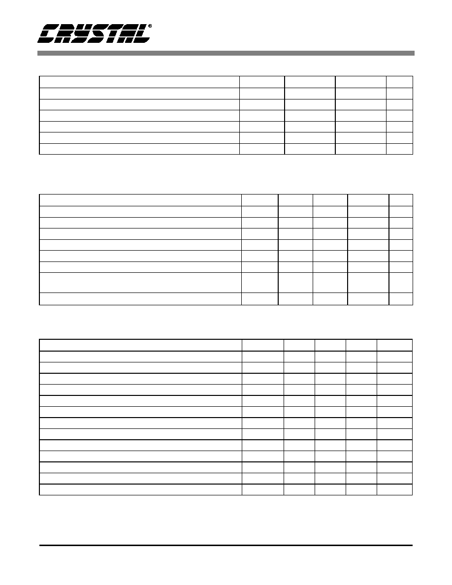
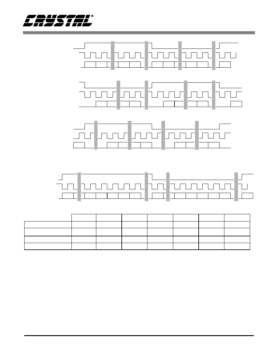
SWITCHING CHARACTERISTICS - SERIAL AUDIO PORTS
(T
A
= 25 ∞C; VA+ = VD+ =
5V ±5%, Inputs: Logic 0 = 0V, Logic 1 = VD+; C
L
= 20 pF)
Notes: 5. The active edges of ISCLK and OSCLK are programmable.
6. The polarity of ILRCK and OLRCK is programmable.
7. This delay is to prevent the previous I/OSCLK edge from being interpreted as the first one after I/OLRCK
has changed.
8. This setup time ensures that this I/OSCLK edge is interpreted as the first one after I/OLRCK has
changed.
Parameter
Symbol Min Typ
Max
Units
OSCLK Active Edge to SDOUT Output Valid
(Note 5)
t
dpd
-
-
20
ns
SDIN Setup TIme Before ISCLK Active Edge
(Note 5)
t
ds
20
-
-
ns
SDIN Hold Time After ISCLK Active Edge
(Note 5)
t
dh
20
-
-
ns
Master Mode
O/RMCK to I/OSCLK active edge delay
(Note 5)
t
smd
0
-
10
ns
O/RMCK to I/OLRCK delay
(Note 6)
t
lmd
0
-
10
ns
I/OSCLK and I/OLRCK Duty Cycle
-
50
-
%
Slave Mode
I/OSCLK Period
t
sckw
36
-
-
ns
I/OSCLK Input Low Width
t
sckl
14
-
-
ns
I/OSCLK Input High Width
t
sckh
14
-
-
ns
I/OSCLK Active Edge to I/OLRCK Edge
(Note 5,6,7)
t
lrckd
20
-
-
ns
I/OLRCK Edge Setup Before I/OSCLK Active Edge (Note 5,6,8)
t
lrcks
20
-
-
ns
sckh
sckl
sckw
t
t
t
tdpd
SDOUT
(input)
(input)
SDIN
dh
t
ds
t
lrcks
t
lrckd
t
ISCLK
OSCLK
ILRCK
OLRCK
ISCLK
OSCLK
ILRCK
OLRCK
(output)
(output)
RMCK
OMCK
(input)
t
smd
t
lmd
Figure 1. Audio Ports Master Mode Timing
Figure 2. Audio Ports Slave Mode and Data I/O
Timing

CS8420
8
DS245PP2
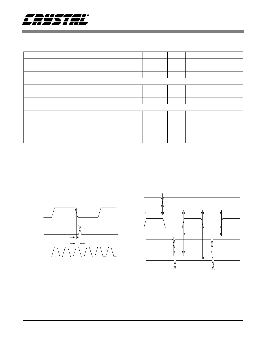
SWITCHING CHARACTERISTICS - CONTROL PORT - SPI MODE
(T
A
= 25 ∞C;
VA+ = VD+ = 5V ±5%, Inputs: Logic 0 = 0V, Logic 1 = VD+; C
L
= 20 pF)
Notes: 9. If Fso or Fsi is lower than 46.875 kHz, then maximum CCLK frequency should be less than 128Fso and
less than 128Fsi. This is dictated by the timing requirements necessary to access the Channel Status
and User Bit buffer memory. Access to the control register file can be carried out at the full 6 MHz rate.
The minimum allowable input sample rate is 8 kHz, so choosing CCLK of less than or equal to
1.024 MHz should be safe for all possible conditions
10. Data must be held for sufficient time to bridge the transition time of CCLK.
11. For f
sck
<1 MHz.
Parameter
Symbol Min Typ
Max
Units
CCLK Clock Frequency
(Note 9)
f
sck
0
-
6.0
MHz
CS High Time Between Transmissions
t
csh
1.0
-
-
µ
s
CS Falling to CCLK Edge
t
css
20
-
-
ns
CCLK Low Time
t
scl
66
-
-
ns
CCLK High Time
t
sch
66
-
-
ns
CDIN to CCLK Rising Setup Time
t
dsu
40
-
-
ns
CCLK Rising to DATA Hold Time
(Note 10)
t
dh
15
-
-
ns
CCLK Falling to CDOUT Stable
t
pd
-
-
45
ns
Rise Time of CDOUT
t
r1
-
-
25
ns
Fall Time of CDOUT
t
f1
-
-
25
ns
Rise Time of CCLK and CDIN
(Note 11)
t
r2
-
-
100
ns
Fall Time of CCLK and CDIN
(Note 11)
t
f2
-
-
100
ns
t r2
t f2
t dsu
t dh
t sch
t scl
CS
CCLK
CDIN
t css
t pd
CDOUT
t csh
Figure 3. SPI Mode Timing
CS8420
DS245PP2
9
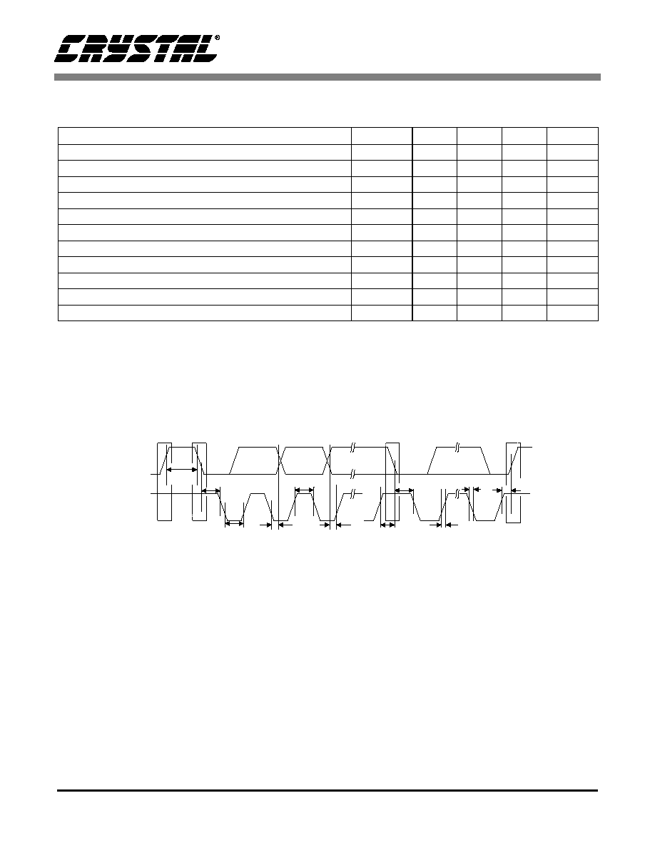
SWITCHING CHARACTERISTICS - CONTROL PORT - I
2
C
Æ
MODE
(Note 12, T
A
=
25 ∞C; VA+ = VD+ = 5V ±5%, Inputs: Logic 0 = 0V, Logic 1 = VD+; C
L
= 20 pF)
Notes: 12. I
2
C is a registered trademark of Philips Semiconductors.
13. Data must be held for sufficient time to bridge the 300ns transition time of SCL.
Specifications are subject to change without notice
Parameter
Symbol Min Typ
Max
Units
SCL Clock Frequency
f
scl
-
-
100
kHz
Bus Free Time Between Transmissions
t
buf
4.7
-
-
µ
s
Start Condition Hold Time (prior to first clock pulse)
t
hdst
4.0
-
-
µ
s
Clock Low Time
t
low
4.7
-
-
µ
s
Clock High Time
t
high
4.0
-
-
µ
s
Setup Time for Repeated Start Condition
t
sust
4.7
-
-
µ
s
SDA Hold Time from SCL Falling
(Note 13)
t
hdd
0
-
-
µ
s
SDA Setup Time to SCL Rising
t
sud
250
-
-
ns
Rise Time of Both SDA and SCL Lines
t
r
-
-
1
µ
s
Fall Time of Both SDA and SCL Lines
t
f
-
-
300
ns
Setup Time for Stop Condition
t
susp
4.7
-
-
µ
s
t
buf
t
hdst
t
hdst
t
low
t r
t f
t
hdd
t
high
t sud
t sust
t susp
Stop
Start
Start
Stop
Repeated
SDA
SCL
Figure 4. I
2
C Mode Timing
CS8420
10
DS245PP2
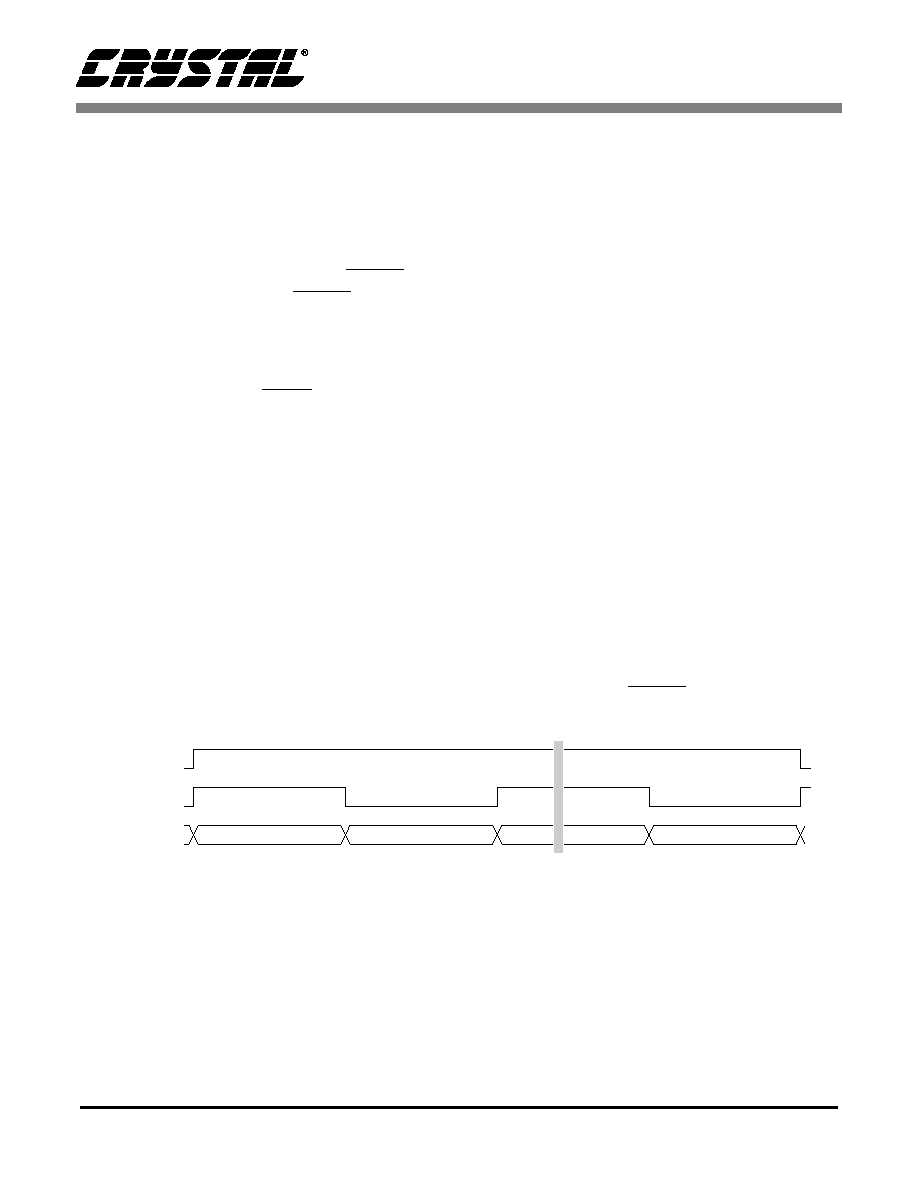
2.
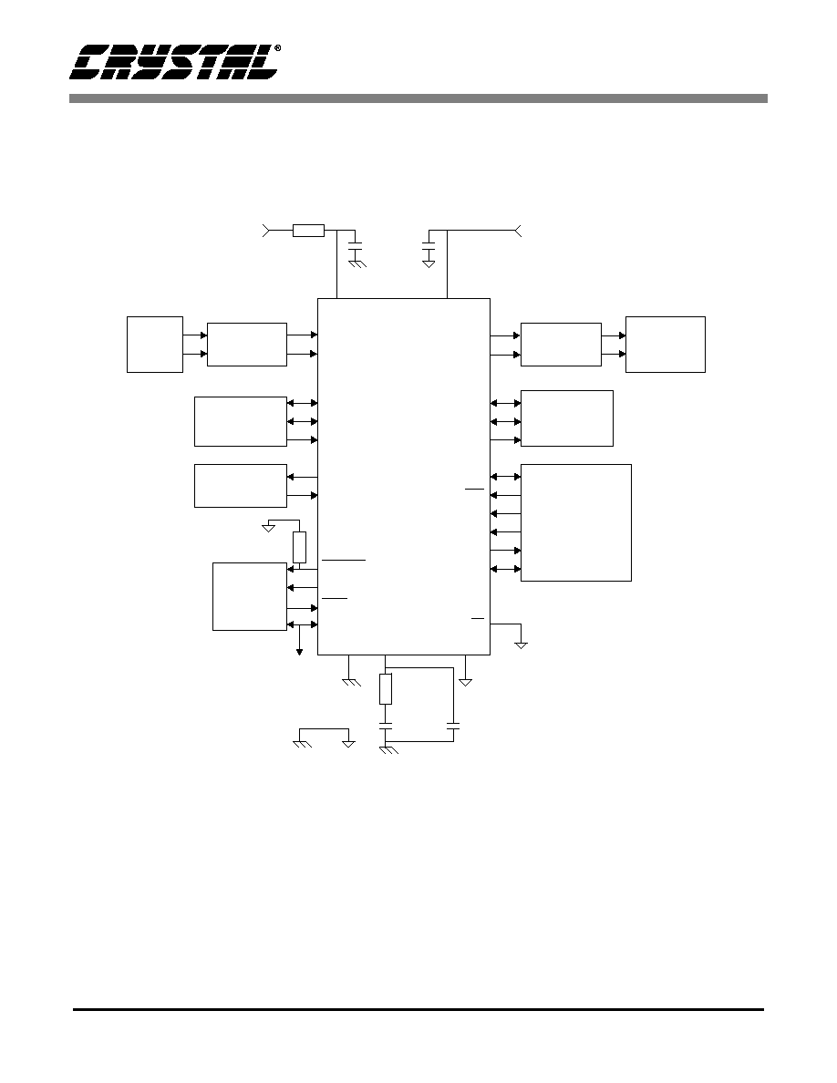
TYPICAL CONNECTION DIAGRAM
CS8420
Cable
Termination
RXP
RXN
AES3/
SPDIF
Source
3-wire Serial
Audio Source
ILRCK
ISCLK
SDIN
Clock Source
and Control
RMCK
OMCK
Hardware
Control
RST
RERR
EMPH
TCBL
To other
CS8420's
Cable
Interface
AES3/
SPDIF
Equipment
TXP
TXN
3-wire Serial
Audio Input
Device
OLRCK
OSCLK
SDOUT
Microcontroller
SDA/CDOUT
AD0/CS
SCL/CCLK
AD1/CDIN
U
INT
VA+
VD+
Ferrite *
Bead
+5V
Analog
Supply *
+5V
Digital
Supply
0.1 F
µ
0.1 F
µ
* A separate analog supply is only necessary in applications where
RMCK is used for a jitter sensitive task. For applications where
RMCK is not used for a jitter sensitive task, connect VA+ to VD+
via a ferrite bead. Keep the decoupling capacitor between VA+
and AGND.
DGND
FILT
AGND
RFILT
CFILT
CRIP
H/S
47k
Figure 5. Recommended Connection Diagram for Software Mode

CS8420
DS245PP2
11
3.
GENERAL DESCRIPTION
The CS8420 is a fully asynchronous sample rate
converter plus AES3 transceiver intended to be
used in digital audio systems. Such systems include
digital mixing consoles, effects processors, tape re-
corders and computer multimedia systems. The
CS8420 is intended for 16, 20, and 24-bit applica-
tions where the input sample rate is unknown, or is
known to be asynchronous to the system sample
rate.
On the input side of the CS8420, AES3 or a 3-wire
serial format can be chosen. The output side pro-
duces both AES3 and a 3-wire serial format. An
I
2
C/SPI compatible microcontroller interface al-
lows full block processing of channel status and
user data via block reads from the incoming AES3
data stream and block writes to the outgoing AES3
data stream. The user can also access information
decoded from the input AES3 data stream, such as
the presence of non-audio data and pre-emphasis,
as well as control the various modes of the device.
For users who prefer not to use a micro-controller,
six hardware modes have been provided, docu-
mented towards the end of this data sheet. In these
modes, flexibility is limited, with pins providing
some programmability.
When used for AES3 in, AES3 out applications, the
CS8420 can automatically transceive user data that
conforms to the IEC60958 recommended format.
The CS8420 also allows access to the relevant bits
in the AES3 data stream to comply with the serial
copy management system (SCMS).
The diagram on the cover of this data sheet shows
the main functional blocks of the CS8420. Figure 5
shows the supply and external connections to the
device.
Familiarity with the AES3 and IEC60958 specifi-
cations are assumed throughout this document. The
Application Note: "Overview of Digital Audio In-
terface Data Structures", contains a tutorial on dig-
ital audio specifications. The paper "An
Understanding and Implementation of the SCMS
Serial Copy Management System for Digital Audio
Transmission", by Clif Sanchez, is an excellent tu-
torial on SCMS. It may be obtained from Crystal
Semiconductor, or from the AES.
To guarantee system compliance, the proper stan-
dards documents should be obtained. The latest
AES3 standard should be obtained from the Audio
Engineering Society or ANSI, the latest IEC60958
standard from the International Electrotechnical
Commission and the latest EIAJ CP-1201 standard
from the Japanese Electronics Bureau.

CS8420
12
DS245PP2
4.
DATA I/O FLOW AND CLOCKING
OPTIONS
The CS8420 can be configured for nine connectiv-
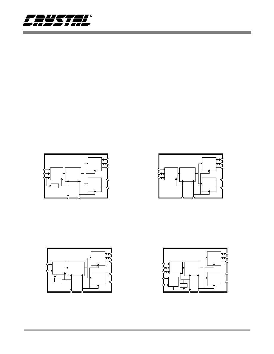
ity alternatives, called data flows. Each data flow
has an associated clocking set-up. Figure 6 shows
the data flow switching, along with the control reg-
ister bits which control the switches; this drawing
only shows the audio data paths for simplicity.
The AESBP switch allows a TTL level, already bi-
phase mark encoded, data stream connected to
RXP to be routed to the TXP and TXN pin drivers.
The TXOFF switch causes the TXP and TXN out-
puts to be driven to ground.
In modes including the SRC function, there are two
audio data related clock domains. One domain in-
cludes the input side of SRC, plus the attached data
source. The second domain includes the output side
of the SRC, plus any attached output ports.
There are two possible clock sources. The first is
known as the recovered clock, is the output of a
PLL, and is connected to the RCMK pin. The input
to the PLL can be either the incoming AES3 data
stream, or the ILRCK word rate clock from the se-
rial audio input port. The second clock is input via
the OMCK pin, and would normally be a crystal
derived stable clock. The Clock Source Control
Register bits determine which clock is connected to
which domain.
By studying the following drawings, and appropri-
ately setting the Data Flow Control and Clock
Source Control register bits, the CS8420 can be
configured to fit a variety of customer require-
ments.
The following drawings illustrate the possible valid
data flows. The audio data flow is indicated by the
thin lines; the clock routing is indicated by the bold
lines. The register settings for the Data Flow Con-
trol register and the Clock Source Register are also
shown for each data flow. Some of the register set-
tings may appear to be not relevant to the particular
data flow in question, but have been assigned a par-
ticular state. This is done to minimize power con-
sumption. The AESBP data path from the RXP pin
to the AES3 output drivers, and the TXOFF con-
trol, have been omitted for clarity, but are present
and functional in all modes where the AES3 trans-
mitter is in use.
Figures 7 and 8 show audio data entering via the se-
rial audio input port, then passing through the sam-
ple rate converter, and then output both to the serial
audio output port and to the AES3 transmitter. Fig-
ure 7 shows the PLL recovering the input clock
from ILRCK word clock. Figure 8 shows using a
Serial
Audio
Input
AES3
Encoder
Serial
Audio
Output
Receiver
Sample
Rate
Converter
RXP
RXN
ILRCK
ISCLK
SDIN
OLRCK
OSCLK
SDOUT
TXP
TXN
AES3
TXOFF
AESBP
SPD1-0
TXD1-0
SRCD
Figure 6. Software Mode Audio Data Flow Switching Options
CS8420
DS245PP2
13
direct 256*Fsi clock input via the RMCK pin, in-
stead of the PLL.
Figure 9 shows audio data entering via the AES3
Receiver. The PLL locks onto the pre-ambles in the
incoming audio stream, and generates a 256*Fsi
clock. The rate converted data is then output via the
serial audio output port and via the AES3 transmit-
ter.
Figure 10 shows the same data flow as Figure 7.
The input clock is derived from an incoming AES3
data stream. The incoming data must be synchro-
nous to the AES3 data stream.
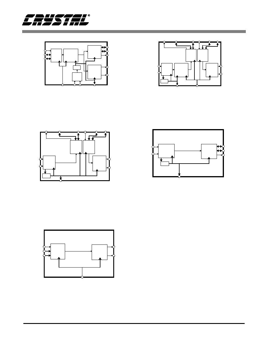
Figure 11 shows the same data flow as Figure 7.
The input data must be synchronous to OMCK.
The output data is clocked by the recovered PLL
clock from an AES3 input stream. This may be
used to implement a "house sync" architecture.
Figure 8 shows audio data entering via the AES3
receiver, passing through the sample rate converter,
and then exiting via the serial audio output port.
Synchronous audio data may then be input via the
serial audio input port and output via the AES3
transmitter.
Figure 13 is the same as Figure 12, but without the
sample rate converter. The whole data path is
clocked via the PLL generated recovered clock.
Figure 14 illustrates a standard AES3 receiver
function, with no rate conversion.
Figure 15 shows a standard AES3 transmitter func-
tion, with no rate conversion.
Figure 7. Serial Audio Input, using PLL, SRC enabled
Figure 8. Serial Audio Input, No PLL, SRC enabled
Serial
Audio
Input
AES3
Encoder
& Driver
Serial
Audio
Output
Sample
Rate
Converter
ILRCK
ISCLK
SDIN
OLRCK
OSCLK
SDOUT
TXP
TXN
PLL
RMCK
OMCK
TXD1-0:
SPD1-0:
SRCD:
OUTC:
INC:
RXD1-0:
00
00
0
0
0
00
Clock Source Control Bits
Data Flow Control Bits
Serial
Audio
Input
AES3
Encoder
& Driver
Serial
Audio
Output
Sample
Rate
Converter
ILRCK
ISCLK
SDIN
OLRCK
OSCLK
SDOUT
TXP
TXN
RMCK
OMCK
TXD1-0:
SPD1-0:
SRCD:
OUTC:
INC:
RXD1-0:
00
00
0
0
0
10
Clock Source Control Bits
Data Flow Control Bits
AES3
Encoder
& Driver
Serial
Audio
Output
Sample
Rate
Converter
OLRCK
OSCLK
SDOUT
TXP
TXN
PLL
RMCK
OMCK
TXD1-0:
SPD1-0:
SRCD:
OUTC:
INC:
RXD1-0:
00
00
1
0
0
01
Clock Source Control Bits
Data Flow Control Bits
AES3
Rx &
Decode
RXP
RXN
Serial
Audio
Input
AES3
Encoder
& Driver
Serial
Audio
Output
Sample
Rate
Converter
ILRCK
ISCLK
SDIN
OLRCK
OSCLK
SDOUT
TXP
TXN
PLL
RMCK OMCK
TXD1-0:
SPD1-0:
SRCD:
OUTC:
INC:
RXD1-0:
00
00
0
0
0
01
Clock Source Control Bits
Data Flow Control Bits
AES3
Rx
RXP
RXN
Figure 9. AES3 Input, SRC enabled
Figure 10. Serial Audio Input, AES3 Input Clock
CS8420
14
DS245PP2
Figure 11. Serial Audio Input, SRC Output clocked by
AES3 Recovered Clock
Figure 12. AES3 Input, SRC to Serial Audio Output,
Serial Audio Input to AES3 Out
AES3
Encoder
& Driver
Serial
Audio
Output
Sample
Rate
Converter
TXP
TXN
PLL
RMCK
OMCK
TXD1-0:
SPD1-0:
SRCD:
OUTC:
INC:
RXD1-0:
01
00
1
0
0
01
Clock Source Control Bits
Data Flow Control Bits
AES3
Rx &
Decode
RXP
RXN
Serial
Audio
Input
OLRCK
OSCLK
SDOUT
ILRCK
ISCLK
SDIN
Serial
Audio
Input
AES3
Encoder
& Driver
Serial
Audio
Output
Sample
Rate
Converter
ILRCK
ISCLK
SDIN
OLRCK
OSCLK
SDOUT
TXP
TXN
PLL
RMCK
OMCK
TXD1-0:
SPD1-0:
SRCD:
OUTC:
INC:
RXD1-0:
00
00
0
1
1
01
Clock Source Control Bits
Data Flow Control Bits
AES3
Rx
RXP RXN
Figure 13. AES3 Input to Serial Audio Output, Serial
Audio Input to AES3 Out, no SRC
Figure 14. AES3 Input to Serial Audio Output Only
AES3
Encoder
& Driver
Serial
Audio
Output
OLRCK
OSCLK
SDOUT
TXP
TXN
PLL
RMCK
TXD1-0:
SPD1-0:
SRCD:
OUTC:
INC:
RXD1-0:
01
10
0
1
0
01
Clock Source Control Bits
Data Flow Control Bits
AES3
Rx &
Decode
RXP
RXN
Serial
Audio
Input
ILRCK
ISCLK
SDIN
Serial
Audio
Output
OLRCK
OSCLK
SDOUT
PLL
RMCK
TXD1-0:
SPD1-0:
SRCD:
TXOFF:
OUTC:
INC:
RXD1-0:
10
10
0
1
1
0
01
Clock Source Control Bits
Data Flow Control Bits
AES3
Rx &
Decode
RXP
RXN
Serial
Audio
Input
AES3
Encoder
& Driver
ILRCK
ISCLK
SDIN
TXP
TXN
OMCK
TXD1-0:
SPD1-0:
SRCD:
OUTC:
INC:
RXD1-0:
01
01
0
0
1
00
Clock Source Control Bits
Data Flow Control Bits
Figure 15. Input Serial Port to AES3 Transmitter

CS8420
DS245PP2
15
5.
SAMPLE RATE CONVERTER (SRC)
Multirate digital signal processing techniques are
used to conceptually upsample the incoming data
to very high rate and then downsample to the out-
going rate, resulting in a 24 bit output, regardless of
the width of the input. The filtering is designed so
that a full input audio bandwidth of 20 kHz is pre-
served if the input sample and output sample rates
are greater than 44.1 kHz. When the output sample
rate becomes less than the input sample rate, the in-
put is automatically bandlimited to avoid aliasing
products in the output. Careful design ensures min-
imum ripple and distortion products are added to
the incoming signal. The SRC also determines the
ratio between the incoming and outgoing sample
rates, and sets the filter corner frequencies appro-
priately. Any jitter in the incoming signal has little
impact on the dynamic performance of the rate con-
verter, and has no influence on the output clock.
5.1
Dither
When using the AES3 input, and when using the
serial audio input port in left justified and I
2
S
modes, all input data is treated as 24-bits wide. Any
truncation that has been done prior to the CS8420
to less than 24-bits should have been done using an
appropriate dither process. If the serial audio input
port is used to feed the SRC, and the port is in right
justified mode, then the input data will be truncated
to the SIRES bit setting value. If SIRES bits are set
to 16 or 20-bits, and the input data is 24-bits wide,
then truncation distortion will occur. Similarly, in
any serial audio input port mode, if an inadequate
number of bit clocks are entered (say 16 instead of
20), then the input words will be truncated, causing
truncation distortion at low levels. In summary,
there is no dithering mechanism on the input side of
the CS8420, and care must be taken to ensure that
no truncation occurs.
Dithering is used internally where appropriate in-
side the SRC block.
The output side of the SRC can be set to 16, 20 or
24 bits. Optional dithering can be applied, and is
automatically scaled to the selected output word
length. This dither is not correlated between left
and right channels. It is recommended that the dith-
er control bit be left in its default on state.
5.2
SRC Locking, Varispeed and the
Sample Rate Ratio Register
The SRC calculates the ratio between the input
sample rate and the output sample rate, and uses
this information to set up various parameters inside
the SRC block. The SRC takes some time to make
this calculation. For a worst case 3:1 to 1:3 input
sample rate transition, the SRC will take 9400/Fso
to settle (195 ms at Fso of 48 kHz). For a power-up
situation, the SRC will start from 1:1, the worst
case time becomes 8300/Fso (172 ms at Fso of
48 kHz).
If the PLL is in use (either AES3 or serial input
port), then the worst case locking time for the PLL
and the SRC is the sum of each locking time.
If Fsi is changing, for example in a varispeed appli-
cation, the REUNLOCK interrupt will occur, and
the SRC will track the incoming sample rate. Dur-
ing this tracking mode, the SRC will still rate con-
vert the audio data, but at increased distortion
levels. Once the incoming sample rate is stable,
then the REUNLOCK interrupt will become false,
and the SRC will return to normal levels of audio
quality.
The VFIFO interrupt occurs if the data buffer in the
SRC overflows, which can occur if the input sam-
ple rate changes at >10%/second.
Varispeed at Fsi slew rates approaching 10%/sec is
only supported when the input is via the serial au-
dio input port. When using the AES3 input, high
frame rate slew rates will cause the PLL to lose
lock.
The sample rate ratio is also made available as a
register, accessible via the control port. The upper

CS8420
16
DS245PP2
2 bits of this register form the integer part of the ra-
tio, while the lower 6 bits form the fractional part.
Since, in many instances, Fso is known, this allows
the calculation of the incoming sample rate by the
host microcontroller.
6.
THREE-WIRE SERIAL AUDIO
PORTS
A 3-wire serial audio input port and a 3-wire serial
audio output port is provided. Each port can be ad-
justed to suit the attached device via control regis-
ters. The following parameters are adjustable:
master or slave, serial clock frequency, audio data
resolution, left or right justification of the data rel-
ative to left/right clock, optional 1 bit cell delay of
the 1st data bit, the polarity of the bit clock and the
polarity of the left/right clock. By setting the appro-
priate control bits, many formats are possible.
Figure 16 shows a selection of common input for-
mats, along with the control bit settings. The clock-
ing of the input section of the CS8420 may be
derived from the incoming ILRCK word rate clock,
using the on-chip PLL. The PLL operation is de-
scribed in the AES receiver description on page 19.
In the case of use with the serial audio input port,
the PLL locks onto the leading edges of the ILRCK
clock.
Figure 17 shows a selection of common output for-
mats, along with the control bit settings. A special
AES3 direct output format is included, which al-
lows serial output port access to the V, U, and C
bits embedded in the serial audio data stream. The
P bit is replaced by a bit indicating the location of
the start of a block. This format is only available
when the serial audio output port is being clocked
by the AES3 receiver recovered clock. Also, the re-
ceived channel status block start signal is only
available in hardware mode 5, as the RCBL pin.
In master mode, the left/right clock and the serial
bit clock are outputs, derived from the appropriate
clock domain master clock.
In slave mode, the left/right clock and the serial bit
clock are inputs. The left/right clock must be syn-
chronous to the appropriate master clock, but the
serial bit clock can be asynchronous and discontin-
uous if required. By appropriate phasing of the
left/right clock and control of the serial clocks,
multiple CS8420's can share one serial port. The
left/right clock should be continuous, but the duty
cycle does not have to be 50%, provided that
enough serial clocks are present in each phase to
clock all the data bits. When in slave mode, the se-
rial audio output port must be set to left justified or
I
2
S data.
When using the serial audio output port in slave
mode with an OLRCK input which is asynchro-
nous to the port's data source, then an interrupt bit
is provided to indicate when repeated or dropped
samples occur.
The CS8420 allows immediate mute of the serial
audio output port audio data via a control register
bit.

CS8420
DS245PP2
17
ILRCK
ISCLK
SDIN
2
Left
Justified
(In)
MSB
LSB
Left
Right
MSB
I S
(In)
Right
Justified
(In)
MSB
LSB
MSB
LSB
MSB
Left
Right
MSB
LSB
MSB
LSB
Left
Right
LSB
MSB
LSB
ILRCK
ISCLK
SDIN
ILRCK
ISCLK
SDIN
Figure 16. Serial Audio Input Example Formats
X = don't care to match format, but does need to be set to the desired setting
+ I
2
S can accept an arbitrary number of bits, determined by the number of ISCLK cycles
* not 11 - See Serial Input Port Data Format Register Bit Descriptions for an explanation of the meaning of each bit
SIMS
SISF
SIRES1/0
SIJUST
SIDEL
SISPOL
SILRPOL
Left Justified
X
X
00
0
0
0
0
I
2
S
X
X
00+
0
1
0
1
Right Justified
X
X
XX*
1
0
0
0
CS8420
18
DS245PP2
MSB
LSB
Left
Right
MSB
I S
(Out)
Right
Justified
(Out)
OLRCK
OSCLK
SDOUT
OLRCK
OSCLK
SDOUT
2
MSB
LSB
MSB
LSB
MSB
Left
Right
Left
Justified
(Out)
MSB
LSB
OLRCK
OSCLK
SDOUT
MSB
LSB
Left
Right
LSB
MSB
LSB
OLRCK
OSCLK
SDOUT
MSB
LSB
MSB
Left
Right
AES3
Direct
(Out)
V
P
U
C
LSB
LSB
V
P
U
C
Figure 17. Serial Audio Output Example Formats
X = don't care to match format, but does need to be set to the desired setting
* not 11 - See Serial Output Data Format Register Bit Descriptions for an explanation of the meaning of each bit
SOMS
SOSF
SORES1/0
SOJUST
SODEL
SOSPOL
SOLRPOL
Left Justified
X
X
XX*
0
0
0
0
I
2
S
X
X
XX*
0
1
0
1
Right Justified
1
X
XX*
1
0
0
0
AES3 Direct
X
X
11
0
0
0
0

CS8420
DS245PP2
19
7.
AES3 TRANSMITTER AND
RECEIVER
The CS8420 includes an AES3 type digital audio
receiver and an AES3 type digital audio transmit-
ter. A comprehensive buffering scheme provides
read/write access to the channel status and user da-
ta. This buffering scheme is described in the Ap-
pendix: Channel Status and User Data Buffer
Management on page 72.
7.1
AES3 Receiver
The AES3 receiver accepts and decodes audio and
digital data according to the AES3, IEC60958
(S/PDIF), and EIAJ CP-1201 interface standards.
The receiver consists of a differential input stage,
accessed via pins RXP and RXN, a PLL based
clock recovery circuit, and a decoder which sepa-
rates the audio data from the channel status and
user data.
External components are used to terminate and iso-
late the incoming data cables from the CS8420.
These components are detailed in the Appendix
"External AES/SPDIF/IEC60958 Transmitter and
Receiver Components" on page 70.
7.1.1
PLL, Jitter Attenuation, and
Varispeed
An on-chip Phase Locked Loop (PLL) is used to re-
cover the clock from the incoming data stream. Al-
though the on-chip sample rate converter is
immune to large amounts of jitter, there are some
applications where low jitter in the recovered
clock, presented on the RMCK pin, is important.
For this reason, the PLL has been designed to have
good jitter attenuation characteristics, shown in
Figures 18, 19 & 20. In addition, the PLL has been
designed to only use the preambles of the AES3
stream to provide lock update information to the
PLL. This results in the PLL being immune to data
dependent jitter affects, since the AES3 preambles
do not vary with the data. The PLL has the ability
to lock onto a wide range of input sample rates,
with no external component changes. If the sample
rate of the input subsequently changes, for example
in a varispeed application, then the PLL will only
track up to ±12.5% from the nominal center sample
rate. The nominal center sample rate is the sample
rate that the PLL first locks onto upon application
of an AES3 data stream, or after enabling the
CS8420 clocks by setting the RUN control bit. If
the 12.5% sample rate limit is exceeded, the PLL
will return to its wide lock range mode, and re-ac-
quire a new nominal center sample rate.

CS8420
20
DS245PP2
Figure 18. Jitter Attenuation Characteristics of PLL
with "slow" Filter Components
Figure 19. Jitter Attenuation Characteristics of PLL
with "medium" Filter Components
-60
-50
-40
-30
-20
-10
0
10
1
10
100
1000
10000
100000
Jitter Frequency (Hz)
J
i
tte
r
A
tte
n
u
a
tio
n
(d
B
)
-60
-50
-40
-30
-20
-10
0
10
1
10
100
1000
10000
100000
Jitter Frequency (Hz)
J
i
tte
r
A
tte
n
u
a
tio
n
(d
B
)
-60
-50
-40
-30
-20
-10
0
10
1
10
100
1000
10000
100000
Jitter Frequency (Hz)
J
i
tte
r
A
tte
n
u
a
tio
n
(d
B
)
Figure 20. Jitter Attenuation Characteristics of PLL
with "fast" Filter Components

CS8420
DS245PP2
21
8.
OMCK OUT ON RMCK
A special mode is available that allows the clock
that is being input through the OMCK pin to be out-
put through the RMCK pin. This feature is con-
trolled by the SWCLK bit in register 4 of the
control registers. When the PLL loses lock the fre-
quency of the VCO drops to 300 kHz. The SWCLK
function allows the clock from RMCK to be used
as a clock in the system without any disruption
when input is removed from the Receiver.
9.
PLL EXTERNAL COMPONENTS
The PLL behavior is affected by the external filter
component values. Figure 5 shows the configura-
tion of the required 2 capacitors and 1 resistor. Two
alternate sets of component values are recommend-
ed, depending on the requirements of the applica-
tion (see Table 1). The default set, called "fast",
accommodates input sample rates of 16 kHz to
108 Hz with no component changes. It has the
highest corner frequency jitter attenuation curve,
and takes the shortest time to lock. The alternate
component set, called "medium" allows the lowest
input sample rate to be 8 kHz, and increases the
lock time of the PLL. Lock times are worst case for
an Fsi transition of 96 kHz.
9.1
Error Reporting and Hold Function
While decoding the incoming AES3 data stream,
the CS8420 can identify several kinds of error, in-
dicated in the Receiver Error register. The UN-
LOCK bit indicates whether the PLL is locked to
the incoming AES3 data. The V bit reflects the cur-
rent validity bit status. The CONF (confidence) bit
indicates the amplitude of the eye pattern opening,
indicating a link that is close to generating errors.
The BIP (bi-phase) error bit indicates an error in in-
coming bi-phase coding. The PAR (parity) bit indi-
cates a received parity error.
The error bits are "sticky": they are set on the first
occurrence of the associated error, and will remain
set until the user reads the register via the control
port. This enables the register to log all unmasked
errors that occurred since the last time the register
was read.
The Receiver Error Mask register allows masking
of individual errors. The bits in this register serve
as masks for the corresponding bits of the Receiver
Error Register. If a mask bit is set to 1, the error is
considered unmasked, meaning that its occurrence
will be reported in the receiver error register, will
affect the RERR pin, will invoke the occurrence of
a RERR interrupt, and will affect the current audio
sample according to the status of the HOLD bits.
The HOLD bits allow a choice of holding the pre-
vious sample, replacing the current sample with
zero (mute), or do not change the current audio
sample. If a mask bit is set to 0, the error is consid-
ered masked, meaning that its occurrence will not
be reported in the receiver error register, will not
induce a pulse on RERR or generate a RERR inter-
rupt, and will not affect the current audio sample.
The QCRC and CCRC errors do not affect the cur-
rent audio sample, even if unmasked.
9.2
Channel Status Data Handling
The first 2 bytes of the Channel Status block are de-
coded into the Receiver Channel Status register.
The setting of the CHS bit in the Channel Status
Data Buffer Control register determines whether
Type
RFILT (k
)
CFILT (
µ
F)
CRIP (nF)
Fsi Range (kHz)
PLL Lock Time (ms)
Medium
0.909
1.8
33
8 to 96
56
Fast
1.78
0.47
8.2
16 to 108
15
Table 1. PLL External Component Values
CS8420
22
DS245PP2
the channel status decodes are from the A channel
(CHS = 0) or B channel (CHS = 1).
The PRO (professional) bit is extracted directly.
Also, for consumer data, the COPY (copyright) bit
is extracted, and the category code and L bits are
decoded to determine SCMS status, indicated by
the ORIG (original) bit. Finally, the AUDIO bit is
extracted, and used to set an AUDIO indicator, as
described in the Non-Audio Auto Detection section
below.
If 50/15 µs pre-emphasis is detected, then this is re-
flected in the state of the EMPH pin.
The encoded sample word length channel status
bits are decoded according to AES3-1992 or IEC
60958. If the AES3 receiver is the data source for
the SRC, then the SRC audio input data is truncated
according to the channel status word length set-
tings. Audio data routed to the serial audio output
port is unaffected by the word length settings; all
24 bits are passed on as received.
The Appendix: Channel Status and User Data Buff-
er Management (page 72) describes the overall
handling of CS and U data.
9.3
User Data Handling
The incoming user data is buffered in a user acces-
sible buffer. Various automatic modes of re-trans-
mitting received U data are provided. The
Appendix: Channel Status and User Data Buffer
Management (page 72) describes the overall han-
dling of CS and U data.
Received U data may also be output to the U pin,
under the control of a control register bit. Depend-
ing on the data flow and clocking options selected,
there may not be a clock available to qualify the U
data output. Figure 21 illustrates the timing.
If the incoming user data bits have been encoded as
Q-channel subcode, then the data is decoded and
presented in 10 consecutive register locations. An
interrupt may be enabled to indicate the decoding
of a new Q-channel block, which may be read via
the control port.
9.4
Non-Audio Auto Detection
Since it is possible to convey non-audio data in an
AES3 data stream, it is important to know whether
the incoming AES3 data stream is digital audio or
not. This information is typically conveyed in
channel status bit 1 (AUDIO), which is extracted
RCBL
out
VLRCK
C, U
Output
RCBL and C output are only available in hardware mode 5.
RCBL goes high 2 frames after receipt of a Z pre-amble, and is high for 16 frames.
VLRCK is a virtual word clock, which may not exist, but is used to illustrate the CU timing.
VLRCK duty cycle is 50%. VLRCK frequency is always equal to the incoming frame rate.
If no SRC is used, and the serial audio output port is in master mode, VLRCK = OLRCK.
If the serial audio output port is in slave mode, then VLRCK needs to be externally created, if required.
C, U transitions are aligned within 1% of VLRCK period to VLRCK edges
±
Figure 21. AES3 Receiver Timing for C & U pin output data

CS8420
DS245PP2
23
automatically by the CS8420. However, certain
non-audio sources, such as AC3 or MPEG encod-
ers, may not adhere to this convention, and the bit
may not be properly set. The CS8420 AES3 receiv-
er can detect such non-audio data. This is accom-
plished by looking for a 96-bit sync code,
consisting of 0x0000, 0x0000, 0x0000, 0x0000,
0xF872, and 0x4E1F. When the sync code is de-
tected, an internal AUTODETECT signal will be
asserted. If no additional sync codes are detected
within the next 4096 frames, AUTODETECT will
be de-asserted until another sync code is detected.
The AUDIO bit in the Receiver Channel Status reg-
ister is the logical OR of AUTODETECT and the
received channel status bit 1. If non-audio data is
detected, the data is still processed exactly as if it
were normal audio. It is up to the user to mute the
outputs as required.
9.5
AES3 Transmitter
The AES3 transmitter encodes and transmits audio
and digital data according to the AES3, IEC60958
(S/PDIF), and EIAJ CP-1201 interface standards.
Audio and control data are multiplexed together
and bi-phase mark encoded. The resulting bit
stream is then driven directly, or through a trans-
former, to an output connector.
The transmitter is usually clocked from the output
side clock domain of the sample rate converter.
This clock may be derived from the clock input pin
OMCK, or from the incoming data. In data flows
with no SRC, and where OMCK is asynchronous to
the data source, an interrupt bit is provided that will
go high every time a data sample is dropped or re-
peated.
The channel status (C) and user channel (U) bits in
the transmitted data stream are taken from storage
areas within the CS8420. The user can manipulate
the contents of the internal storage with a micro-
controller. The CS8420 will also run in one of sev-
eral automatic modes. The Appendix: Channel Sta-
tus and User Data Buffer Management (page 72)
provides detailed descriptions of each automatic
mode, and describes methods for accessing the
storage areas. The transmitted user data can option-
ally be input via the U pin, under the control of a
control port register bit. Figure 22 shows the timing
requirements for inputting U data via the U pin.
9.5.1
Transmitted Frame and Channel
Status Boundary Timing
The TCBL pin may be an input or an output, and is
used to control or indicate the start of transmitted
channel status block boundaries.
In some applications, it may be necessary to control
the precise timing of the transmitted AES3 frame
boundaries. This may be achieved in 3 ways:
a) With TCBL configured as an input, when TCBL
transitions high for >3 OMCK clocks, it will cause
a frame start, and a new channel status block start.
b) If the AES3 output comes from the AES3 input,
while there is no SRC, setting TCBL as output will
cause AES3 output frame boundaries to align with
AES3 input frame boundaries.
c) If the AES3 output comes from the serial audio
input port while the port is in slave mode, and
TCBL is set to output, then the start of the A chan-
nel sub-frame will be aligned with the leading edge
of ILRCK.
9.5.2
TXN and TXP Drivers
The line drivers are low skew, low impedance, dif-
ferential outputs capable of driving cables directly.
Both drivers are set to ground during reset (RST =
low), when no AES3 transmit clock is provided,
and optionally under the control of a register bit.
The CS8420 also allows immediate mute of the
AES3 transmitter audio data via a control register
bit.
External components are used to terminate and iso-
late the external cable from the CS8420. These
components are detailed in the Appendix "External

CS8420
24
DS245PP2
AES/SPDIF/IEC60958 Transmitter and Receiver
Components" on page 70.
9.6
Mono Mode Operation
Currently, the AES3 standard is being updated to
include options for 96 kHz sample rate operation.
One method is to double the frame rate of the cur-
rent format. This results in a 96 kHz sample rate,
stereo signal carried over a single twisted pair ca-
ble. An alternate method is where the 2 sub-frames
in a 48 kHz frame rate AES3 signal are used to car-
ry consecutive samples of a mono signal, resulting
in a 96 kHz sample rate stream. This allows older
equipment, whose AES3 transmitters and receivers
are not rated for 96 kHz frame rate operation, to
handle 96 kHz sample rate information. In this
"mono mode", 2 AES3 cables are needed for stereo
data transfer. The CS8420 offers mono mode oper-
ation, both for the AES3 receiver and for the AES3
transmitter. Figure 23 shows the operation of mono
mode in comparison with normal stereo mode. The
receiver and transmitter sections may be indepen-
dently set to mono mode via the MMR and MMT
control bits.
The receiver mono mode effectively doubles Fsi
compared to the input frame rate. The clock output
on the RMCK pin tracks Fsi, and so is doubled in
frequency compared to stereo mode. In mono
mode, A and B sub-frames are routed to the SRC
inputs as consecutive samples.
When the transmitter is in mono mode, either A or
B SRC consecutive outputs are routed alternately
to A and B sub-frames in the AES3 output stream.
Which channel status block is transmitted is also
selectable.
For the AES3 input to serial audio port output data
flow, in receiver mono mode, then the receiver will
TCBL
in or out
VLRCK
Tsetup = >7.5% AES3 frame time
Thold = 0
AES3 Transmitter in Stereo Mode
Tsetup = >15% AES3 frame time
Thold = 0
AES3 Transmitter in Mono Mode
TCBL
in or out
VLRCK
U
Input
U
Tsetup
Thold
U
CUV
CUV
CUV
CUV
C, U, V
Input
Tsetup
Thold
VLRCK is a virtual word clock, which may not exist, but is used to illustrate the CUV timing.
VLRCK duty cycle is 50%.
In stereo mode, VLRCK = AES3 frame rate. In mono mode, VLRCK = 2*AES3 frame rate
If the serial audio output port is in master mode, and TCBL is an output, and the SRC is not in use,
then VLRCK = OLRCK.
If the serial audio input port is in master mode, and TCBL is an input, and the SRC is not between
the serial audio input port and the AES3 transmitter, then VLRCK = ILRCK.
Otherwise, VLRCK needs to be externally created, if required
Figure 22. AES3 Transmitter Timing for C, U and V pin input data
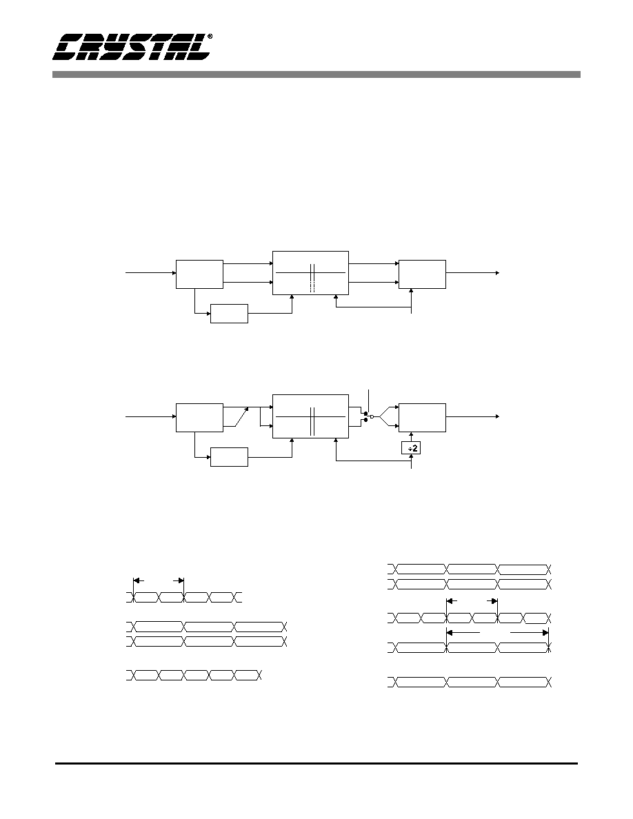
CS8420
DS245PP2
25
run at a frame rate of Fsi/2, and the serial audio out-
put port will run at Fsi. Identical data will appear in
both left and right data fields on the SDOUT pin.
For the serial audio input port to AES3 transmitter
data flow, in transmitter mono mode, then the input
port will run at Fso audio sample rate, while the
AES3 transmitter frame rate will be at Fso/2. The
data from either consecutive left, or right, positions
will be selected for transmitting in A and B sub-
frames.
SRC
AES3
Receiver
AES3
Transmitter
PLL
In
Out
A
A
A
A
B
B
B
B
96kHz stereo
96kHz frame rate
256x96kHz
96kHz stereo
96kHz frame rate
96kHz
Fsi
96kHz
Fso
OMCK (256, 384, or 512x 96kHz)
SRC
AES3
Receiver
AES3
Transmitter
PLL (x2)
In
Out
A
A
A
A
B
B
B
B
96kHz mono
48kHz frame rate
256x96kHz
96kHz mono
48kHz frame rate
96kHz
Fsi
96kHz
Fso
OMCK (256, 384, or 512x 96kHz)
*
+
A & B sub-frames data are time-multiplexed
into consecutive samples
Consecutive samples are alternately routed
to A & B sub-fames
*
+
RECEIVER
MONO MODE
RECEIVER
STEREO MODE
MMTLR
TRANSMITTER
STEREO MODE
TRANSMITTER
MONO MODE
A1
B1
Outgoing
AES3
SRC Aout
SRC Bout
A1
B1
A2
B2
STEREO
MONO
Frame
A2
B2
Outgoing
AES3
A selected
Outgoing
AES3
B selected
A1
A2
B1
B2
Frame
TRANSMITTER TIMING
Figure 23. Mono Mode Operation Compared to Normal Stereo Operation
A1
B1
A2
B2
Incoming
AES3
SRC Ain
SRC Bin
Ain & Bin
SRC
A1
A1
B1
B1
A2
B2
A2
B2
STEREO
MONO
Frame
RECEIVER TIMING

CS8420
26
DS245PP2
10. CONTROL PORT DESCRIPTION
AND TIMING
The control port is used to access the registers, al-
lowing the CS8420 to be configured for the desired
operational modes and formats. In addition, Chan-
nel Status and User data may be read and written
via the control port. The operation of the control
port may be completely asynchronous with respect
to the audio sample rates. However, to avoid poten-
tial interference problems, the control port pins
should remain static if no operation is required.
The control port has 2 modes: SPI and I
2
C, with the
CS8420 acting as a slave device. SPI mode is se-
lected if there is a high to low transition on the
AD0/CS pin, after the RST pin has been brought
high. I
2
C mode is selected by connecting the
AD0/CS pin to VD+ or DGND, thereby perma-
nently selecting the desired AD0 bit address state.
10.1
SPI Mode
In SPI mode, CS is the CS8420 chip select signal,
CCLK is the control port bit clock (input into the
CS8420 from the microcontroller), CDIN is the in-
put data line from the microcontroller, CDOUT is
the output data line to the microcontroller. Data is
clocked in on the rising edge of CCLK and out on
the falling edge.
Figure 24 shows the operation of the control port in
SPI mode. To write to a register, bring CS low. The
first 7 bits on CDIN form the chip address and must
be 0010000. The eighth bit is a read/write indicator
(R/W), which should be low to write. The next 8
bits form the Memory Address Pointer (MAP),
which is set to the address of the register that is to
be updated. The next 8 bits are the data which will
be placed into the register designated by the MAP.
During writes, the CDOUT output stays in the Hi-
Z state. It may be externally pulled high or low with
a 47 k
resistor, if desired.
There is a MAP auto increment capability, enabled
by the INCR bit in the MAP register. If INCR is a
zero, then the MAP will stay constant for succes-
sive read or writes. If INCR is set to a 1, then the
MAP will auto-increment after each byte is read or
written, allowing block reads or writes of succes-
sive registers.
To read a register, the MAP has to be set to the cor-
rect address by executing a partial write cycle
which finishes (CS high) immediately after the
MAP byte. The MAP auto increment bit (INCR)
M A P
MSB
LSB
DATA
b y te 1
b y te n
R/W
R/W
A D D R E S S
C H IP
ADDRESS
C H IP
C D IN
C C L K
CS
C D O U T
MSB
LSB MSB
LSB
0010000
0010000
MAP = Memory Address Pointer, 8 bits, MSB first
High Impedance
Figure 24. Control Port Timing in SPI Mode
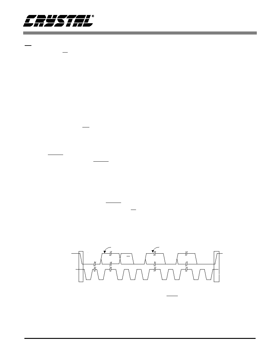
CS8420
DS245PP2
27
may be set or not, as desired. To begin a read, bring
CS low, send out the chip address and set the
read/write bit (R/W) high. The next falling edge of
CCLK will clock out the MSB of the addressed
register (CDOUT will leave the high impedance
state). If the MAP auto increment bit is set to 1, the
data for successive registers will appear consecu-
tively.
10.2
I
2
C
Mode
In I
2
C mode, SDA is a bidirectional data line. Data
is clocked into and out of the part by the clock,
SCL, with the clock to data relationship as shown
in Figure 25. There is no CS pin. Each individual
CS8420 is given a unique address. Pins AD0, AD1
form the 2 least significant bits of the chip address,
and should be connected to VD+ or DGND as de-
sired. The EMPH pin is used to set the AD2 bit, by
connecting a resistor from the EMPH pin to VD+
or to DGND. The state of the pin is sensed while
the CS8420 is being reset. The upper 4 bits of the
7-bit address field are fixed at 0010. To communi-
cate with a CS8420, the chip address field, which is
the first byte sent to the CS8420, should match
0010 followed by the settings of the EMPH, AD1,
and AD0. The eighth bit of the address is the R/W
bit. If the operation is a write, the next byte is the
Memory Address Pointer (MAP) which selects the
register to be read or written. If the operation is a
read, the contents of the register pointed to by the
MAP will be output. Setting the auto increment bit
in MAP allows successive reads or writes of con-
secutive registers. Each byte is separated by an ac-
knowledge bit. The ACK bit is output from the
CS8420 after each input byte is read, and is input to
the CS8420 from the microcontroller after each
transmitted byte. I
2
C is a registered trademark of
Philips Semiconductors.
10.3
Interrupts
The CS8420 has a comprehensive interrupt capa-
bility. The INT output pin is intended to drive the
interrupt input pin on the host microcontroller. The
INT pin may be set to be active low, active high or
active low with no active pull-up transistor. This
last mode is used for active low, wired-OR hook-
ups, with multiple peripherals connected to the mi-
crocontroller interrupt input pin.
Many conditions can cause an interrupt, as listed in
the interrupt status register descriptions. Each
source may be masked off via mask registers. In ad-
dition, each source may be set to rising edge, fall-
ing edge or level sensitive. Combined with the
option of level sensitive or edge sensitive modes
within the microcontroller, many different set-ups
are possible, depending on the needs of the equip-
ment designer.
SDA
SCL
0010
AD2-0
R/W
Start
ACK
DATA7-0
ACK
DATA7-0
ACK
Stop
Note 2
Note 1
Note 1: AD2 is derived from a resistor attached to the EMPH pin,
Note 2: If operation is a write, this byte contains the Memory Address Pointer, MAP
AD1 and AD0 are determined by the state of the corresponding pins
Figure 25. Control Port Timing in
I
2
C
Mode

CS8420
28
DS245PP2
11. CONTROL PORT REGISTER BIT DEFINITIONS
11.1
Memory Address Pointer (MAP)
This register defaults to 01
INCR
Auto Increment Address Control Bit
0 -
Auto increment address off
1 -
Auto increment address on
MAP6-MAP0
Register address and function list
0 - Reserved
1 - Misc. Control 1
2 - Misc. Control 2
3 - Data Flow Control
4 - Clock Source Control
5 - Serial Audio Input Port Data Format
6 - Serial Audio Output Port Data Format
7 - Interrupt Register 1 Status
8 - Interrupt Register 2 Status
9 - Interrupt Register 1 Mask
10 - Interrupt Register1 Mode (MSB)
11 - Interrupt Register 1 Mode (LSB)
12 - Interrupt Register 2 Mask
13 - Interrupt Register 2 Mode (MSB)
14 - Interrupt Register 2 Mode (LSB)
15 - Receiver Channel Status Bits
16 - Receiver Error Status
17 - Receiver Error Mask
18 - Channel Status Data Buffer Control
19 - User Data Buffer Control
20 to 29 - Q-channel Subcode Bytes 0 to 9
30 - Sample Rate Ratio
31 - Reserved
32 to 55 - C-bit or U-bit Data Buffer
56 to 126 - Reserved
127 - Chip ID and version register
Reserved registers must not be written to during normal operation. Some reserved registers are used
for test modes, which can completely alter the normal operation of the CS8420.
7
6
5
4
3
2
1
0
INCR
MAP6
MAP5
MAP4
MAP3
MAP2
MAP1
MAP0

CS8420
DS245PP2
29
Addr
Function
7
6
5
4
3
2
1
0
1
Control 1
SWCLK
VSET
MUTESAO
MUTEAES
DITH
INT1
INT0
TCBLD
2
Control 2
TRUNC
HOLD1
HOLD0
RMCKF
MMR
MMT
MMTCS
MMTLR
3
Data Flow Control
AMLL
TXOFF
AESBP
TXD1
TXD0
SPD1
SPD0
SRCD
4
Clock Source Control
0
RUN
CLK1
CLK0
OUTC
INC
RXD1
RXD0
5
Serial Input Format
SIMS
SISF
SIRES1
SIRES0
SIJUST
SIDEL
SISPOL
SILRPOL
6
Serial Output Format
SOMS
SOSF
SORES1
SORES0
SOJUST
SODEL
SOSPOL
SOLRPOL
7
Interrupt 1 Status
TSLIP
OSLIP
SRE
OVRGL
OVRGR
DETC
EFTC
RERR
8
Interrupt 2 Status
0
0
VFIFO
REUNLOCK
DETU
EFTU
QCH
UOVW
9
Interrupt 1 Mask
TSLIPM
OSLIPM
SREM
OVRGLM
OVRGRM
DETCM
EFTCM
RERRM
10
Interrupt 1 Mode (MSB)
TSLIP1
OSLIP1
SRE1
OVRGL1
OVRGR1
DETC1
EFTC1
RERR1
11
Interrupt 1 Mode (LSB)
TSLIP0
OSLIP0
SRE0
OVRGL0
OVRGR0
DETC0
EFTC0
RERR0
12
Interrupt 2 Mask
0
0
VFIFOM
REUNLOCKM
DETUM
EFTUM
QCHM
UOVWM
13
Interrupt 2 Mode (MSB)
0
0
VFIFO1
REUNLOCK1
DETU1
EFTU1
QCH1
UOVW1
14
Interrupt 2 Mode (LSB)
0
0
VFIFO0
REUNLOCK0
DETU0
EFTU0
QCH0
UOVW0
15
Receiver CS Data
AUX3
AUX2
AUX1
AUX0
PRO
AUDIO
COPY
ORIG
16
Receiver Errors
0
QCRC
CCRC
UNLOCK
V
CONF
BIP
PAR
17
Receiver Error Mask
0
QCRCM
CCRCM
UNLOCKM
VM
CONFM
BIPM
PARM
18
CS Data Buffer Control
0
0
BSEL
CBMR
DETCI
EFTCI
CAM
CHS
19
U Data Buffer Control
0
0
0
UD
UBM1
UBM0
DETUI
EFTUI
20-29 Q sub-code Data
30
Sample Rate Ratio
SRR7
SRR6
SRR5
SRR4
SRR3
SRR2
SRR1
SRR0
32-55 C or U Data Buffer
127
ID and Version
ID3
ID2
ID1
ID0
VER3
VER2
VER1
VER0
Table 2. Summary of all Bits in the Control Register Map

CS8420
30
DS245PP2
11.2
Miscellaneous Control 1 (1)
SWCLK
Controls the output of OMCK on the RMCK pin in the absence of input to the Receiver
0 - RMCK default function
1 - OMCK is switched to output through RMCK in the absence of input to the Receiver
VSET
Transmitted V bit level
0 - Transmit a 0 for the V bit, indicating that the data is valid, and is normally linear PCM
audio (default)
1 - Transmit a 1 for the V bit, indicating that the data is invalid or is not linear PCM audio data
MUTESAO
Mute control for the serial audio output port
0 - Normal output (default)
1 - Mute the serial audio output port
MUTEAES
Mute control for the AES3 transmitter output
0 - Normal output (default)
1 - Mute the AES3 transmitter output
DITH
Dither Control
0 - Triangular PDF dither applied to output data. The level of the dither is
automatically adjusted to be appropriate for the output word length selected by the
SORES bits (default)
1 - No dither applied to output data.
INT1-INT0
Interrupt (INT) output pin control
00 - Active high, high output indicates an interrupt condition has occurred (default)
01 - Active low, low output indicates an interrupt condition has occurred
10 - Open drain, active low. This setting requires an external pull up resistor on the
INT pin.
11 - Reserved
TCBLD
Transmit Channel Status Block pin (TCBL) direction specifier
0 - TCBL is an input (default)
1 - TCBL is an output
7
6
5
4
3
2
1
0
SWCLK
VSET
MUTESAO
MUTEAES
DITH
INT1
INT0
TCBLD

CS8420
DS245PP2
31
11.3
Miscellaneous Control 2 (2)
TRUNC
Determines whether the word length is set according to the incoming Channel Status data
0 - Data to the SRC is not truncated (default)
1 - Data to the SRC is set according to the AUX field in the incoming data stream
HOLD1-0The HOLD bits determine how the received audio sample is affected when a receiver
error occurs.
00 - Hold the last valid audio sample (default)
01 - Replace the current audio sample with 00 (mute)
10 - Do not change the received audio sample
11 - Reserved
RMCKFSelect recovered master clock output pin frequency.
0 - RMCK is equal to 256 * Fsi (default)
1 - RMCK is equal to 128 * Fsi
MMR
Select AES3 receiver mono or stereo operation
0 - Interpret A and B subframes as two independent channels (normal stereo
operation, default)
1 - Interpret A and B subframes as consecutive samples of one channel of data.
This data is duplicated to both left and right parallel outputs of the AES receiver
block. The input sample rate (Fsi) is doubled compared to MMR=0
MMT
Select AES3 transmitter mono or stereo operation
0 - Outputs left channel input into A subframe and right channel input into B subframe
(normal stereo operation, default).
1 - Output either left or right channel inputs into consecutive subframe outputs (mono
mode, left or right is determined by MMTLR bit)
MMTCS
Select A or B channel status data to transmit in mono mode
0 - Use channel A CS data for the A sub-frame slot and use channel B CS data for the
B sub-frame slot (default)
1 - Use the same CS data for both the A and B sub-frame output slots. If MMTLR = 0, use the
left channel CS data. If MMTLR = 1, use the right channel CS data.
MMTLR
Channel Selection for AES Transmitter mono mode
0 - Use left channel input data for consecutive sub-frame outputs (default)
1- Use right channel input data for consecutive sub-frame outputs
7
6
5
4
3
2
1
0
TRUNC
HOLD1
HOLD0
RMCKF
MMR
MMT
MMTCS
MMTLR

CS8420
32
DS245PP2
11.4
Data Flow Control (3)
The Data Flow Control register configures the flow of audio data to/from the following blocks: Serial
Audio Input Port, Serial Audio Output Port, AES3 receiver, AES3 transmitter, and Sample Rate Con-
verter. In conjunction with the Clock Source Control register, multiple Receiver/Transmitter/Trans-
ceiver modes may be selected. The output data should be muted prior to changing bits in this register
to avoid transients.
AMLL
Auto Mutes the SRC data sink when Receiver lock is lost, zero data is transmitted. The SRC
data sink may be either, or both, the Transmitter and the Serial Audio Output Port.
0 - Disables Auto Mute on loss of lock (default)
1 - Enables Auto Mute on loss of lock
TXOFF
AES3 Transmitter Output Driver Control
0 - AES3 transmitter output pin drivers normal operation (default)
1 - AES3 transmitter output pin drivers drive to 0V.
AESBP
AES3 bypass mode selection
0 - normal operation
1 - Connect the AES3 transmitter driver input directly to the RXP pin, which become
a normal TTL threshold digital input.
TXD1 - TXD0
AES3 Transmitter Data Source
00 - SRC output (default)
01 - Serial audio input port
10 - AES3 receiver
11 - Reserved
SPD1 - SPD0
Serial Audio Output Port Data Source
00 - SRC output (default)
01 - Serial Audio Input Port
10 - AES3 receiver
11 - Reserved
SRCD
Input Data Source for SRC
0 - Serial Audio Input Port (default)
1 - AES3 Receiver
7
6
5
4
3
2
1
0
AMLL
TXOFF
AESBP
TXD1
TXD0
SPD1
SPD0
SRCD

CS8420
DS245PP2
33
11.5
Clock Source Control (4)
This register configures the clock sources of various blocks. In conjunction with the Data Flow Control
register, various Receiver/Transmitter/Transceiver modes may be selected.
RUN
The RUN bit controls the internal clocks, allowing the CS8420 to be placed in a
"powered down", low current consumption, state.
0 - Internal clocks are stopped. Internal state machines are reset. The fully static
control port is operational, allowing registers to be read or changed. Reading and
writing the U and C data buffers is not possible. Power consumption is low (default).
1 - Normal part operation. This bit must be written to the 1 state to allow the CS8420
to begin operation. All input clocks should be stable in frequency and phase when
RUN is set to 1.
CLK1-0
Output side master clock input (OMCK) frequency to output sample rate (Fso) ratio selector. If
these bits are changed during normal operation, then always stop the CS8420 first (RUN = 0),
then write the new value, then start the CS8420 (RUN = 1).
00 - OMCK frequency is 256*Fso(default)
01 - OMCK frequency is 384*Fso
10 - OMCK frequency is 512*Fso
11 - reserved
OUTC
Output Time Base
0 - OMCK input pin (modified by the selected divide ratio bits CLK1 & CLK0,
default)
1 - Recovered Input Clock
INC
Input Time Base Clock Source
0 - Recovered Input Clock (default)
1 - OMCK input pin (modified by the selected divide ratio bits CLK1 & CLK0)
RXD1-0
Recovered Input Clock Source
00 - 256*Fsi, where Fsi is derived from the ILRCK pin (only possible when the
serial audio input port is in slave mode, default)
01 - 256*Fsi, where Fsi is derived from the AES3 input frame rate
10 - Bypass the PLL and apply an external 256*Fsi clock via the RMCK pin. The AES3
receiver is held in synchronous reset. This setting is useful to prevent UNLOCK
interrupts when using an external RMCK and inputting data via the serial audio
input port.
11 - Reserved
7
6
5
4
3
2
1
0
0
RUN
CLK1
CLK0
OUTC
INC
RXD1
RXD0

CS8420
34
DS245PP2
11.6
Serial Audio Input Port Data Format (5)
SIMS
Master/Slave Mode Selector
0 - Serial audio input port is in slave mode (default)
1 - Serial audio input port is in master mode
SISF
ISCLK frequency (for master mode)
0 - 64*Fsi (default)
1 - 128*Fsi
SIRES1-0
Resolution of the input data, for right-justified formats
00 - 24 bit resolution (default)
01 - 20 bit resolution
10 - 16 bit resolution
11 - Reserved
SIJUST
Justification of SDIN data relative to ILRCK
0 - Left-justified (default)
1 - Right-justified
SIDEL
Delay of SDIN data relative to ILRCK, for left-justified data formats
0 - MSB of SDIN data occurs in the first ISCLK period after the ILRCK edge (default)
1 - MSB of SDIN data occurs in the second ISCLK period after the ILRCK edge
SISPOL
ISCLK clock polarity
0 - SDIN sampled on rising edges of ISCLK (default)
1 - SDIN sampled on falling edges of ISCLK
SILRPOL
ILRCK clock polarity
0 - SDIN data is for the left channel when ILRCK is high (default)
1 - SDIN data is for the right channel when ILRCK is high
7
6
5
4
3
2
1
0
SIMS
SISF
SIRES1
SIRES0
SIJUST
SIDEL
SISPOL
SILRPOL

CS8420
DS245PP2
35
11.7
Serial Audio Output Port Data Format (6)
SOMS
Master/Slave Mode Selector
0 - Serial audio output port is in slave mode (default)
1 - Serial audio output port is in master mode
SOSF
OSCLK frequency (for master mode)
0 - 64*Fso (default)
1 - 128*Fso
SORES1-0
Resolution of the output data on SDOUT and on the AES3 output
00 - 24 bit resolution (default)
01 - 20 bit resolution
10 - 16 bit resolution
11 - Direct copy of the received NRZ data from the AES3 receiver (including C, U, and
V bits, the time slot normally occupied by the P bit is used to indicate the location
of the block start, SDOUT pin only, serial audio output port clock must be derived
from the AES3 receiver recovered clock)
SOJUST
Justification of SDOUT data relative to OLRCK
0 - Left-justified (default)
1 - Right-justified (master mode only)
SODEL
Delay of SDOUT data relative to OLRCK, for left-justified data formats
0 - MSB of SDOUT data occurs in the first OSCLK period after the OLRCK edge
(default)
1 - MSB of SDOUT data occurs in the second OSCLK period after the OLRCK edge
SOSPOL
OSCLK clock polarity
0 - SDOUT transitions occur on falling edges of OSCLK (default)
1 - SDOUT transitions occur on rising edges of OSCLK
SOLRPOL
OLRCK clock polarity
0 - SDOUT data is for the left channel when OLRCK is high (default)
1 - SDOUT data is for the right channel when OLRCK is high
7
6
5
4
3
2
1
0
SOMS
SOSF
SORES1
SORES0
SOJUST
SODEL
SOSPOL
SOLRPOL

CS8420
36
DS245PP2
11.8
Interrupt 1 Register Status (7) (Read Only)
For all bits in this register, a "1" means the associated interrupt condition has occurred at least once
since the register was last read. A "0" means the associated interrupt condition has NOT occurred
since the last reading of the register. Reading the register resets all bits to 0, unless the interrupt mode
is set to level and the interrupt source is still true. Status bits that are masked off in the associated
mask register will always be "0" in this register. This register defaults to 00.
TSLIP
AES3 transmitter source data slip interrupt. In data flows with no SRC, and where OMCK, which
clocks the AES3 transmitter, is asynchronous to the data source, this bit will go high every time
a data sample is dropped or repeated. Also, when TCBL is an input, and when the SRC is not
in use, this bit will go high on receipt of a new TCBL signal.
OSLIP
Serial audio output port data slip interrupt. When the serial audio output port is in slave mode,
and OLRCK is asynchronous to the port data source, this bit will go high every time a data sam-
ple is dropped or repeated. Also, when the SRC is used, and the SRC output goes to the output
serial port configured in slave mode, this bit will indicate if the ratio of OMCK frequency to OL-
RCK frequency does not match what is set in the CLK1 and CLK0 bits.
SRE
Sample rate range exceeded indicator. Occurs if Fsi/Fso or Fso/Fsi exceeds 3.
OVRGL
Over-range indicator for left (A) channel SRC output. Occurs on internal over-range for left
channel data. Note that the CS8420 automatically clips over-ranges to plus or minus full-scale.
OVRGR
Over-range indicator for right (B) channel SRC output. Occurs on internal over-range for right
channel data. Note that the CS8420 automatically clips over-ranges to plus or minus full-scale
DETC
D to E C-buffer transfer interrupt. The source for this bit is true during the D to E buffer transfer
in the C bit buffer management process.
EFTC
E to F C-buffer transfer interrupt. The source for this bit is true during the E to F buffer transfer
in the C bit buffer management process.
RERR
A receiver error has occurred. The Receiver Error register may be read to determine the nature
of the error which caused the interrupt.
7
6
5
4
3
2
1
0
TSLIP
OSLIP
SRE
OVRGL
OVRGR
DETC
EFTC
RERR

CS8420
DS245PP2
37
11.9
Interrupt Register 2 Status (8) (Read Only)
For all bits in this register, a "1" means the associated interrupt condition has occurred at least once
since the register was last read. A "0" means the associated interrupt condition has NOT occurred
since the last reading of the register. Reading the register resets all bits to 0, unless the interrupt mode
is set to level and the interrupt source is still true. Status bits that are masked off in the associated
mask register will always be "0" in this register. This register defaults to 00.
VFIFO
Varispeed FIFO overflow indicator. Occurs if the data buffer in the SRC overflows. This will oc-
cur if the input sample rate slows too fast.
REUNLOCK
Sample rate converter unlock indicator. This interrupt occurs if the SRC is still tracking a chang-
ing input or output sample rate.
DETU
D to E U-buffer transfer interrupt. The source of this bit is true during the D to E buffer transfer
in the U bit buffer management process (block mode only).
EFTU
E to F U-buffer transfer interrupt. The source of this bit is true during the E to F buffer transfer
in the U bit buffer management process (block mode only).
QCH
A new block of Q-subcode data is available for reading. The data must be completely read with-
in 588 AES3 frames after the interrupt occurs to avoid corruption of the data by the next block.
UOVW
U-bit FIFO Overwrite. This interrupt occurs on an overwrite in the U-bit FIFO.
11.10 Interrupt 1 Register Mask (9)
The bits of this register serve as a mask for the Interrupt 1 Register. If a mask bit is set to 1, the error
is considered unmasked, meaning that its occurrence will affect the INT pin and the status register. If
a mask bit is set to 0, the error is considered masked, meaning that its occurrence will not affect the
INT pin or the status register. The bit positions align with the corresponding bits in Interrupt Register
1. This register defaults to 00.
11.11 Interrupt Register 1 Mode Registers MSB & LSB(10,11)
The two Interrupt Mode registers form a 2-bit code for each Interrupt Register 1 function. This code
determines whether the INT pin is set active on the arrival of the interrupt condition, on the removal
of the interrupt condition, or on the continuing occurrence of the interrupt condition. These registers
default to 00.
00 - Rising edge active
01 - Falling edge active
10 - Level active
11 - Reserved
7
6
5
4
3
2
1
0
0
0
VFIFO
REUNLOCK
DETU
EFTU
QCH
UOVW
7
6
5
4
3
2
1
0
TSLIPM
OSLIPM
SREM
OVRGLM
OVRGRM
DETCM
EFTCM
RERRM
7
6
5
4
3
2
1
0
TSLIP1
OSLIP1
SRE1
OVRGL1
OVRGR1
DETC1
EFTC1
RERR1
TSLIP0
OSLIP0
SRE0
OVRGL0
OVRGR0
DETC0
EFTC0
RERR0

CS8420
38
DS245PP2
11.12 Interrupt 2 Register Mask (12)
The bits of this register serve as a mask for the Interrupt 2 Register. If a mask bit is set to 1, the error
is considered unmasked, meaning that its occurrence will affect the INT pin and the status register. If
a mask bit is set to 0, the error is considered masked, meaning that its occurrence will not affect the
INT pin or the status register. The bit positions align with the corresponding bits in Interrupt Register
2. This register defaults to 00.
11.13 Interrupt Register 2 Mode Registers MSB & LSB(13,14)
The two Interrupt Mode registers form a 2-bit code for each Interrupt 2 register function. This code
determines whether the INT pin is set active on the arrival of the interrupt condition, on the removal
of the interrupt condition, or on the continuing occurrence of the interrupt condition. These registers
default to 00.
00 - Rising edge active
01 - Falling edge active
10 - Level active
11 - Reserved
7
6
5
4
3
2
1
0
0
0
VFIFOM
REUNLOCKM
DETUM
EFTUM
QCHM
UOVWM
7
6
5
4
3
2
1
0
0
0
VFIFO1
REUNLOCK1
DETU1
EFTU1
QCH1
UOVW1
0
0
VFIFO0
REUNLOCK0
DETU0
EFTU0
QCH0
UOVW0

CS8420
DS245PP2
39
11.14 Receiver Channel Status (15) (Read Only)
The bits in this register can be associated with either channel A or B of the received data. The desired
channel is selected with the CHS bit of the Channel Status Data Buffer Control Register.
AUX3-0
The AUX3-0 bits indicate the width of the incoming auxiliary data field, as indicated by the in-
coming channel status bits, decoded according to IEC60958 and AES3.
0000 - Auxiliary data is not present
0001 - Auxiliary data is 1 bit long
0010 - Auxiliary data is 2 bits long
0011 - Auxiliary data is 3 bits long
0100 - Auxiliary data is 4 bits long
0101 - Auxiliary data is 5 bits long
0110 - Auxiliary data is 6 bits long
0111 - Auxiliary data is 7 bits long
1000 - Auxiliary data is 8 bits long
1001 - 1111 Reserved
PRO
Channel status block format indicator
0 - Received channel status block is in consumer format
1 - Received channel status block is in professional format
AUDIO
Audio indicator
0 - Received data is linearly coded PCM audio
1 - Received data is not linearly coded PCM audio
COPY
SCMS copyright indicator
0 - Copyright asserted
1 - Copyright not asserted
ORIG
SCMS generation indicator. This is decoded from the category code and the L bit.
0 - Received data is 1st generation or higher
1 - Received data is original
Note: COPY and ORIG will both be set to 1 if the incoming data is flagged as professional, or if the receiver is not
in use.
7
6
5
4
3
2
1
0
AUX3
AUX2
AUX1
AUX0
PRO
AUDIO
COPY
ORIG

CS8420
40
DS245PP2
11.15 Receiver Error (16) (Read Only)
This register contains the AES3 receiver and PLL status bits. Unmasked bits will go high on occur-
rence of the error, and will stay high until the register is read. Reading the register resets all bits to 0,
unless the error source is still true. Bits that are masked off in the receiver error mask register will
always be 0 in this register. This register defaults to 00.
QCRCQ-subcode data CRC error has occurred. Updated on Q-subcode block boundaries.
0 - No error
1 - Error
CCRCChannel Status Block Cyclic Redundancy Check bit. Updated on CS block boundaries.
This bit is valid in professional mode only.
0 - No error
1 - Error
UNLOCK
PLL lock status bit. Updated on CS block boundaries.
0 - PLL locked
1 - PLL out of lock
V
Received AES3 Validity bit status. Updated on sub-frame boundaries.
0 - Data is valid and is normally linear coded PCM audio
1 - Data is invalid, or may be valid compressed audio
CONF
Confidence bit. Updated on sub-frame boundaries.
0 - No error
1 - Confidence error. This indicates that the received data eye opening is less than
half a bit period, indicating a poor link that is not meeting specifications.
BIP
Bi-phase error bit. Updated on sub-frame boundaries.
0 - No error
1 - Bi-phase error. This indicates an error in the received bi-phase coding.
PAR
Parity bit. Updated on sub-frame boundaries.
0 - No error
1 - Parity error
11.16 Receiver Error Mask (17)
The bits in this register serve as masks for the corresponding bits of the Receiver Error Register. If a
mask bit is set to 1, the error is considered unmasked, meaning that its occurrence will appear in the
receiver error register, will affect the RERR pin, will affect the RERR interrupt, and will affect the cur-
rent audio sample according to the status of the HOLD bit. If a mask bit is set to 0, the error is con-
sidered masked, meaning that its occurrence will not appear in the receiver error register, will not
affect the RERR pin, will not affect the RERR interrupt, and will not affect the current audio sample.
The CCRC and QCRC bits behave differently from the other bits: they do not affect the current audio
sample even when unmasked. This register defaults to 00.
7
6
5
4
3
2
1
0
0
QCRC
CCRC
UNLOCK
V
CONF
BIP
PAR
7
6
5
4
3
2
1
0
0
QCRCM
CCRCM
UNLOCKM
VM
CONFM
BIPM
PARM

CS8420
DS245PP2
41
11.17 Channel Status Data Buffer Control (18)
BSEL
Selects the data buffer register addresses to contain User data or Channel Status data
0 - Data buffer address space contains Channel Status data (default)
1 - Data buffer address space contains User data
CBMR
Control for the first 5 bytes of channel status "E" buffer
0 - Allow D to E buffer transfers to overwrite the first 5 bytes of channel status data
(default)
1 - Prevent D to E buffer transfers from overwriting first 5 bytes of channel status data
DETCI
D to E C-data buffer transfer inhibit bit.
0 - Allow C-data D to E buffer transfers (default)
1 - Inhibit C-data D to E buffer transfers
EFTCI
E to F C-data buffer transfer inhibit bit.
0 - Allow C-data E to F buffer transfers (default)
1 - Inhibit C-data E to F buffer transfers
CAM
C-data buffer control port access mode bit
0 - One byte mode
1 - Two byte mode
CHS
Channel select bit
0 - Channel A information is displayed at the EMPH pin and in the receiver channel
status register. Channel A information is output during control port reads when
CAM is set to 0 (One Byte Mode)
1 - Channel B information is displayed at the EMPH pin and in the receiver channel
status register. Channel B information is output during control port reads when
CAM is set to 0 (One Byte Mode)
7
6
5
4
3
2
1
0
0
0
BSEL
CBMR
DETCI
EFTCI
CAM
CHS
CS8420
42
DS245PP2
11.18 User Data Buffer Control (19)
UD
User data pin (U) direction specifier
0 - The U pin is an input. The U data is latched in on both rising and falling edges of
OLRCK. This setting also chooses the U pin as the source for transmitted
U data (default).
1 - The U pin is an output. The received U data is clocked out on both rising and falling edges
of ILRCK. This setting also chooses the U data buffer as the source of transmitted
U data.
UBM1-0
Sets the operating mode of the AES3 U bit manager
00 - Transmit all zeros mode (default)
01 - Block mode
10 - Reserved
11 - IEC consumer mode 4
DETUI
D to E U-data buffer transfer inhibit bit (valid in block mode only).
0 - Allow U-data D to E buffer transfers (default)
1 - Inhibit U-data D to E buffer transfers
EFTUI
E to F U-data buffer transfer inhibit bit (valid in block mode only).
0 - Allow U-data E to F buffer transfers (default)
1 - Inhibit U-data E to F buffer transfer
11.19 Q-Channel Subcode Bytes 0 to 9 (20 - 29) (Read Only)
The following 10 registers contain the decoded Q-channel subcode data
7
6
5
4
3
2
1
0
0
0
0
UD
UBM1
UBM0
DETUI
EFTUI
7
6
5
4
3
2
1
0
ADDRESS
ADDRESS
ADDRESS
ADDRESS
CONTROL
CONTROL
CONTROL
CONTROL
TRACK
TRACK
TRACK
TRACK
TRACK
TRACK
TRACK
TRACK
INDEX
INDEX
INDEX
INDEX
INDEX
INDEX
INDEX
INDEX
MINUTE
MINUTE
MINUTE
MINUTE
MINUTE
MINUTE
MINUTE
MINUTE
SECOND
SECOND
SECOND
SECOND
SECOND
SECOND
SECOND
SECOND
FRAME
FRAME
FRAME
FRAME
FRAME
FRAME
FRAME
FRAME
ZERO
ZERO
ZERO
ZERO
ZERO
ZERO
ZERO
ZERO
ABS MINUTE
ABS MINUTE
ABS MINUTE
ABS MINUTE
ABS MINUTE
ABS MINUTE
ABS MINUTE
ABS MINUTE
ABS SECOND
ABS SECOND
ABS SECOND
ABS SECOND
ABS SECOND
ABS SECOND
ABS SECOND
ABS SECOND
ABS FRAME
ABS FRAME
ABS FRAME
ABS FRAME
ABS FRAME
ABS FRAME
ABS FRAME
ABS FRAME

CS8420
DS245PP2
43
11.20 Sample Rate Ratio (30) (Read Only)
The Sample Rate Ratio is Fso divided by Fsi. This value is represented as an integer and a fractional
part. The value is meaningful only after the both the PLL and SRC have reached lock, and the SRC
output is being used
SRR7-6The integer part of the sample rate ratio
SRR5-0 The fractional part of the sample rate ratio
11.21 C-bit or U-bit Data Buffer (32 - 55)
Either channel status data buffer E or user data buffer E (provided UBM bits are set to block mode)
is accessible via these register addresses.
11.22 CS8420 I.D. and Version Register (127) (Read Only)
ID3-0
ID code for the CS8420. Permanently set to 0001
VER3-0
CS8420 revision level. Revision B is coded as 0001, Revision C is coded as 0011,
Revision D is coded as 0100
7
6
5
4
3
2
1
0
SRR7
SRR6
SRR5
SRR4
SRR3
SRR2
SRR1
SRR0
7
6
5
4
3
2
1
ID3
ID3
ID2
ID1
ID0
VER3
VER2
VER1
VER0
CS8420
44
DS245PP2
12. SYSTEM AND APPLICATIONS
ISSUES
12.1
Reset, Power Down and Start-up
Options
When RST is low, the CS8420 enters a low power
mode and all internal states are reset, including the
control port and registers, and the outputs are mut-
ed. When RST is high, the control port becomes
operational and the desired settings should be load-
ed into the control registers. Writing a 1 to the RUN
bit will then cause the part to leave the low power
state and begin operation. After the PLL and the
SRC have settled, the AES3 and serial audio out-
puts will be enabled.
Some options within the CS8420 are controlled by
a start-up mechanism. During the reset state, some
of the output pins are reconfigured internally to be
inputs. Immediately upon exiting the reset state, the
level of these pins is sensed. The pins are then
switched to be outputs. This mechanism allows
output pins to be used to set alternative modes in
the CS8420 by connecting a 47k
resistor to be-
tween the pin and either VD+ (HI) or DGND (LO).
For each mode, every start-up option select pin
MUST have an external pull-up or pull-down resis-
tor. In software mode, the only start-up option pin
is EMPH, which is used to set a chip address bit for
the control port in I
2
C mode. Hardware modes use
many start-up options, which are detailed in the
hardware definition section at the end of this data
sheet.
12.2
ID Code and Revision Code
The CS8420 has a register that contains a 4-bit
code to indicate that the addressed device is a
CS8420. This is useful when other CS84XX family
members are resident in the same system, allowing
common software modules.
The CS8420 4-bit revision code is also available.
This allows the software driver for the CS8420 to
identify which revision of the device is in a partic-
ular system, and modify its behavior accordingly.
To allow for future revisions, it is strongly recom-
mend that the revision code is read into a variable
area within the microcontroller, and used wherever
appropriate as revision details become known.
12.3
Power Supply, Grounding, and PCB
layout
For most applications, the CS8420 can be operated
from a single +5V supply, following normal supply
decoupling practice (see Figure 5. "Recommended
Connection Diagram for Software Mode" on page
10). For applications where the recovered input
clock, output on the RMCK pin, is required to be
low jitter, then use a separate, quiet, analog +5V
supply for VA+, decoupled to AGND. In addition,
a separate region of analog ground plane around the
FILT, AGND, VA+, RXP and RXN pins is recom-
mended.
The VD+ supply should be well decoupled with a
0.1
µ
F capacitor to DGND to minimize AES3 trans-
mitter induced transients.
Extensive use of power and ground planes, ground
plane fill in unused areas and surface mount decou-
pling capacitors are recommended. Make sure de-
coupling capacitors are mounted on the same side
of the board as the CS8420, to minimize via induc-
tance effects. All decoupling capacitors should be
as close to the CS8420 as possible.

CS8420
DS245PP2
45
12.4
Synchronization of Multiple CS8420s
The serial audio output ports of multiple CS8420s
can be synchronized by sharing the same master
clock, OSCLK, OLRCK, and RST line and ensur-
ing that all devices leave the reset state on the same
master clock falling edge. Either all the ports need
to be in slave mode, or one can be set as a master.
The AES3 transmitters may be synchronized by
sharing the same master clock, TCBL, and RST
signals, and all devices leave the reset state on the
same master clock falling edge. The TCBL pin is
used to synchronize multiple CS8420 AES3 trans-
mitters at the channel status block boundaries. One
CS8420 must have its TCBL set to master; the oth-
ers must be set to slave TCBL. Alternatively,
TCBL can be derived from some external logic, in
which case all the CS8420 devices should be set to
slave TCBL.
12.5
Extended Range Sample Rate
Conversion
For handling sampling rate conversion ratios great-
er than 3:1 or less than 1:3, the user can use a cas-
cade of two devices. The product of the conversion
ratio of the two devices should equal the target con-
version ratio.
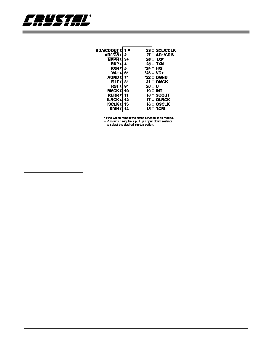
CS8420
46
DS245PP2
13. SOFTWARE MODE - PIN DESCRIPTION
The above diagram and the following pin descriptions apply to software mode. In hardware
mode, some pins change their function as described in subsequent sections of this data sheet.
Fixed function pins are marked with a *, and will be described once in this section. Pins marked
with a + are used upon reset to select various start-up options, and require a pull-up or pull-
down resistor.
Power Supply Connections:
VD+ - Positive Digital Power *
Positive supply for the digital section. Nominally +5V.
VA+ - Positive Analog Power *
Positive supply for the analog section. Nominally +5V. This supply should be as quiet as possible since
noise on this pin will directly affect the jitter performance of the recovered clock.
DGND - Digital Ground *
Ground for the digital section. DGND should be connected to the same ground as AGND.
AGND - Analog Ground *
Ground for the analog section. AGND should be connected to the same ground as DGND.
Clock Related Pins:
OMCK - Output Section Master Clock Input
Output section master clock input. The frequency must be 256x, 384x, or 512x the output sample rate
(Fso).
RMCK - Input Section Recovered Master Clock Output
Input section recovered master clock output. Will be at a frequency of 128x or 256x the input sample
rate (Fsi).
FILT - PLL Loop Filter *
An RC network should be connected between this pin and ground. Recommended schematic and
component values are given in the Receiver section of this data sheet.

CS8420
DS245PP2
47
Overall Device Control:
H/S - Hardware or Software Control Mode Select *
The H/S pin determines the method of controlling the operation of the CS8420, and the method of
accessing CS and U data. In software mode, device control and CS and U data access is primarily via
the control port, using a microcontroller. In hardware mode, alternate modes and access to CS and U
data is provided by pins. This pin should be permanently tied to VD+ or DGND.
RST - Reset Input *
When RST is low, the CS8420 enters a low power mode and all internal states are reset. On initial
power up, RST must be held low until the power supply is stable, and all input clocks are stable in
frequency and phase. This is particularly true in hardware mode with multiple CS8420 devices, where
synchronization between devices is important.
INT - Interrupt Output
The INT output pin indicates errors and key events during the operation of the CS8420. All bits affecting
INT are maskable via control registers. The condition(s) that initiated interrupt are readable via a control
register. The polarity of the INT output, as well as selection of a standard or open drain output, is set via
a control register. Once set true, the INT pin goes false only after the interrupt status registers have
been read, and the interrupt status bits have returned to zero.
Audio Input Interface:
SDIN - Serial Audio Input Port Data Input
Audio data serial input pin.
ISCLK - Serial Audio Input Port Bit Clock input or output
Serial bit clock for audio data on the SDIN pin.
ILRCK - Serial Audio Input Port Left/Right Clock input or output
Word rate clock for the audio data on the SDIN pin. The frequency will be at the input sample rate (Fsi)
AES3/SPDIF Receiver Interface:
RXP, RXN - Differential Line Receiver Inputs
Differential line receiver inputs, carrying AES3 type data.
RERR - Receiver Error Indicator
When high, indicates a problem with the operation of the AES3 receiver. The status of this pin is
updated once per sub-frame of incoming AES3 data. Conditions that can cause RERR to go high are:
validity, parity error, bi-phase coding error, confidence, QCRC and CCRC errors, as well as loss of lock
in the PLL. Each condition may be optionally masked from affecting the RERR pin using the Receiver
Error Mask Register. The RERR pin tracks the status of the unmasked errors: the pin goes high as soon
as an unmasked error occurs and goes low immediately when all unmasked errors go away.
EMPH - Pre-emphasis Indicator Output
EMPH is low when the incoming AES3 data indicates the presence of 50/15
µ
s pre-emphasis. When
the AES3 data indicates the absence of pre-emphasis or the presence of other than 50/15
µ
s pre-
emphasis EMPH is high. This is also a start-up option pin, and requires a 47 k
resistor to either VD+
or DGND, which determines the AD2 address bit for the control port in I
2
C mode.
Audio Output Interface:
SDOUT - Serial Audio Output Port Data Output
Audio data serial output pin.

CS8420
48
DS245PP2
OSCLK - Serial Audio Output Port Bit Clock input or output
Serial bit clock for audio data on the SDOUT pin.
OLRCK - Serial Audio Output Port Left/Right Clock input or output
Word rate clock for the audio data on the SDOUT pin. The frequency will be at the output sample rate
(Fso)
AES3/SPDIF Transmitter Interface:
TCBL - Transmit Channel Status Block Start
This pin can be configured as an input or output. When operated as output, TCBL is high during the first
sub-frame of a transmitted channel status block, and low at all other times. When operated as input,
driving TCBL high for at least three OMCK (or RMCK, depending on which clock is operating the AES3
encoder block) clocks will cause the next transmitted sub-frame to be the start of a channel status
block.
TXN, TXP - Differential Line driver outputs
Differential line driver outputs, transmitting AES3 type data. Drivers are pulled to low while the CS8420
is in the reset state.
Control Port Signals:
SCL/CCLK - Control Port clock
SCL/CCLK is the serial control interface clock, and is used to clock control data bits into and out of the
CS8420.
AD0/CS - Address Bit 0 (I
2
C) / Control Port Chip Select (SPI)
A falling edge on this pin puts the CS8420 into SPI control port mode. With no falling edge, the CS8420
defaults to I
2
C mode. In I
2
C mode, AD0 is a chip address pin. In SPI mode, CS is used to enable the
control port interface on the CS8420.
AD1/CDIN - Address Bit 1 (I
2
C) / Serial Control data in (SPI)
In I
2
C mode, AD1 is a chip address pin. In SPI mode, CDIN is the input data line for the control port
interface
SDA/CDOUT - Serial Control Data I/O (I
2
C) / data out (SPI)
In I
2
C mode, SDA is the control I/O data line. SDA is open drain, and requires an external pull-up
resistor to VD+. In SPI mode, CDOUT is the output data from the control port interface on the CS8420.
Miscellaneous pins:
U - User Data
The U pin may optionally be used to input User data for transmission by the AES3 transmitter, see
Figure 22 for timing information. Alternatively, the U pin may be set to output User data from the AES3
receiver, see Figure 21 for timing information. If not driven, a 47k
pull-down resistor is recommended
for the U pin, since the default state of the UD direction bit sets the U pin as an input. The pull-down
resistor ensures that the transmitted user data will be zero. If the U pin is always set to be an output,
thereby causing the U bit manager to be the source of the U data, then the resistor is not necessary.
The U pin should not be tied directly to ground, in case it is programmed to be an output, and
subsequently tries to output a logic high. This situation may affect the long term reliability of the device.
If the U pin is driven by a logic level output, then a 100
series resistor is recommended.

CS8420
DS245PP2
49
14. HARDWARE MODES
14.1
Overall Description
The CS8420 has six hardware modes, which allow
use of the device without using a micro-controller
to access the device control registers and CS & U
data. The flexibility of the CS8420 is necessarily
limited in hardware mode. Various pins change
function in hardware mode, and various data paths
are also possible. These alternatives are identified
by hardware mode numbers 1 through 6. The fol-
lowing sections describe the data flows and pin def-
initions for each hardware mode.
14.1.1
Hardware Mode Definitions
Hardware mode is selected by connecting the H/S
pin to `1'. In hardware mode, 3 pins (DFC0, DFC1
& S/AES) determine the hardware mode number,
according to Table 3Start-up options are used ex-
tensively in hardware mode. Options include
whether the serial audio output ports are master or
slave, the serial audio ports' format and whether
TCBL is an input or an output. Which output pins
are used to set which modes depends on which
hardware mode is being used.
14.1.2
Serial Audio Port Formats
In hardware mode, only a limited number of alter-
native serial audio port formats are available. These
formats are described by Tables 4 & 5, which de-
fine the equivalent software mode bit settings for
each format. Timing diagrams are shown in Figures
16 and 17.
For each hardware mode, the following pages con-
tain a data flow diagram, a pin-out drawing, a pin
descriptions list and a definition of the available
start-up options.
DFC1 DFC0 S/AES
Hardware Mode Number
0
0
0
1 - Default Data Flow, AES3 input
0
0
1
2 - Default Data Flow, serial input
0
1
-
3 - Transceive Flow, with SRC
1
0
-
4 - Transceive Flow, no SRC
1
1
0
5 - AES3 Rx only, AES3 input
1
1
1
6 - AES3 Tx only, serial input
Table 3. Hardware Mode Definitions
SOSF SORES1/0 SOJUST SODEL SOSPOL SOLRPOL
OF1 - Left Justified
0
00
0
0
1
0
OF2 - I
2
S 24-bit data
0
00
0
1
0
1
OF3 - Right Justified, master
mode only
0
00
1
0
0
0
OF4 - I
2
S 16 bit data
0
10
0
1
0
1
OF5 - Direct AES3 data
0
11
0
0
1
0
Table 4. Serial Audio Output Formats Available in Hardware Mode
SISF
SIRES1/0 SIJUST
SIDEL
SISPOL
SILRPOL
IF1 - Left Justified
0
00
0
0
1
0
IF2 - I
2
S
0
00
0
1
0
1
IF3 - Right Justified
24-bit data
0
00
1
0
0
0
IF4 - Right Justified
16-bit data
0
10
1
0
0
0
Table 5. Serial Audio Input Formats Available in Hardware Mode
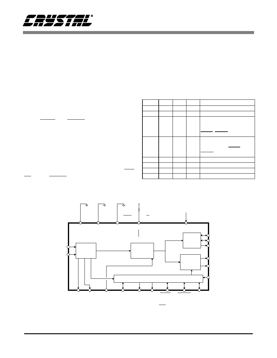
CS8420
50
DS245PP2
14.2
Hardware Mode 1 Description
(DEFAULT Data Flow, AES3 Input)
Hardware Mode 1 data flow is shown in Figure 26.
Audio data is input via the AES3 receiver, and rate
converted. The audio data at the new rate is then
output both via the serial audio output port and via
the AES3 transmitter.
The channel status data, user data and validity bit
information are handled in 2 alternative modes: 1A
and 1B, determined by a start-up resistor on the
COPY pin. In mode 1A, the received PRO, COPY,
ORIG, EMPH, and AUDIO channel status bits are
output on pins. The transmitted channel status bits
are copied from the received channel status data,
and the transmitted U and V bits are 0.
In mode 1B, only the COPY and ORIG pins are
output, and reflect the received channel status data.
The transmitted channel status bits, user data and
validity bits are input serially via the PRO/C, EM-
PH/U and AUDIO/V pins. Figure 22 shows the
timing requirements.
Start-up options are shown in Table 6, and allow
choice of the serial audio output port as a master or
slave, choice of 4 serial audio output port formats,
and the source for transmitted C, U and V data. The
following pages contain the detailed pin descrip-
tions for hardware mode 1.
If a validity, parity, bi-phase or lock receiver error
occurs, the current audio sample will be held.
AES3
Encoder
& Tx
Serial
Audio
Output
AES3 Rx
&
Decoder
Sample
Rate
Converter
C & U bit Data Buffer
Clocked by
Output Clock
Clocked by
Input Derived Clock
RXP
RXN
OLRCK
OSCLK
SDOUT
TXP
TXN
RMCK
RERR
COPY ORIG EMPH/U
TCBLD
PRO/C
AUDIO/V
TCBL
MUTE
DFC0
DFC1
S/AES
VD+
H/S
Output
Clock
Source
OMCK
Power supply pins (VD+, VA+, DGND, AGND), the reset pin (RST) and the PLL filter pin (FILT)
are omitted from this diagram. Please refer to the Typical Connection Diagram for hook-up details.
Figure 26. Hardware Mode 1 - Default Data Flow, AES3 Input
SDOUT RMCK RERR COPY
Function
LO
-
-
-
Serial Output Port is Slave
HI
-
-
-
Serial Output Port is Master
-
-
-
LO
Mode1A: C transmitted data
is copied from received data,
U & V = 0, received PRO,
EMPH, AUDIO are visible.
-
-
-
HI
Mode 1B: CUV transmitted
data is input serially on pins,
received PRO, EMPH,
AUDIO are not visible
-
LO
LO
Serial Output Format OF1
-
LO
HI
Serial Output Format OF2
-
HI
LO
Serial Output Format OF3
-
HI
HI
Serial Output Format OF4
Table 6. Hardware Mode 1 Start-up Options
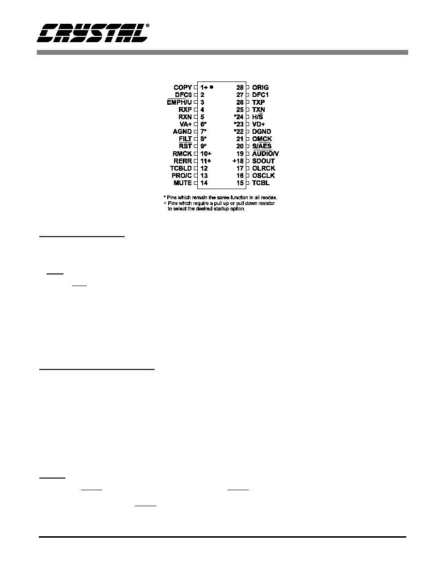
CS8420
DS245PP2
51
14.2.1
Pin Description - Hardware Mode 1
Overall Device Control:
DFC0, DFC1 - Data Flow Control Inputs
DFC0 and DFC1 inputs determine the major data flow options available in hardware mode, according to
Table 3.
S/AES - Serial Audio or AES3 Input Select
S/AES is connected to ground in hardware mode 1, in order to select the AES3 input.
MUTE - Mute Output Data Input
If MUTE is low, audio data is passed normally. If MUTE is high, then both the AES3 transmitted audio
data and the serial audio output port data is set to digital zero.
OMCK - Output Section Master Clock Input
Output section master clock input. The frequency must be 256x the output sample rate (Fso).
AES3/SPDIF Receiver Interface:
RXP, RXN - Differential Line Receiver Inputs
Differential line receiver inputs, carrying AES3 type data.
RMCK - Input Section Recovered Master Clock Output
Input section recovered master clock output. Will be at a frequency of 256x the input sample rate (Fsi).
This is also a start-up option pin, and requires a pull-up or pull-down resistor.
RERR - Receiver Error Indicator
When high, indicates a problem with the operation of the AES3 receiver. The status of this pin is
updated once per sub-frame of incoming AES3 data. Conditions that cause RERR to go high are: parity
error, and bi-phase coding error, as well as loss of lock in the PLL. This is also a start-up option pin,
and requires a pull-up or pull-down resistor.
EMPH/U - Pre-emphasis Indicator Output or U-bit Data Input
The EMPH/U pin reflects either the state of the EMPH channel status bits in the incoming AES3 type
data stream, or is the serial U-bit input for the AES3 type transmitted data, clocked by OLRCK. When
indicating emphasis EMPH/U is low if the incoming data indicates 50/15
µ
s pre-emphasis and high
otherwise.

CS8420
52
DS245PP2
COPY - Copy Channel Status Bit Output
The COPY pin reflects the state of the COPY Channel Status bit in the incoming AES3 type data
stream. This is also a start-up option pin, and requires a pull-up or pull-down resistor.
ORIG - Original Channel Status Output
SCMS generation indicator. This is decoded from the incoming category code and the L bit. A low
output indicates that the audio data stream is 1st generation or higher. A high indicates that the audio
data stream is original.
PRO/C - Professional Channel Status Bit Output or C-bit Data Input
The PRO/C pin either reflects the state of the Professional/Consumer Channel Status bit in the incoming
AES3 type data stream, or is the serial C-bit input for the AES3 type transmitted data, clocked by
OLRCK.
AUDIO/V - Audio Channel Status Bit Output or V-bit Data Input
The AUDIO/V pin either reflects the state of the audio/non audio Channel Status bit in the incoming
AES3 type data stream, or is the V-bit data input for the AES3 type transmitted data stream, clocked by
OLRCK.
Audio Output Interface:
SDOUT - Serial Audio Output Port Data Output
Audio data serial output pin. This is also a start-up option pin, and requires a pull-up or pull-down
resistor.
OSCLK - Serial Audio Output Port Bit Clock Input or Output
Serial bit clock for audio data on the SDOUT pin.
OLRCK - Serial Audio Output Port Left/Right Clock Input or Output
Word rate clock for the audio data on the SDOUT pin. The frequency will be at the output sample rate
(Fso)
AES3/SPDIF Transmitter Interface:
TCBL - Transmit Channel Status Block Start
When operated as output, TCBL is high during the first sub-frame of a transmitted channel status block,
and low at all other times. When operated as input, driving TCBL high for at least three OMCK clocks
will cause the current transmitted sub-frame to be the start of a channel status block.
TCBLD - Transmit Channel Status Block Direction Input
Connect TCBLD to VD+ to set TCBL as an output. Connect TCBLD to DGND to set TCBL as an input.
TXN, TXP - Differential Line Driver Outputs
Differential line driver outputs, transmitting AES3 type data. Drivers are pulled to low while the CS8420
is in the reset state.

CS8420
DS245PP2
53
14.3
Hardware Mode 2 Description
(DEFAULT Data Flow, Serial Input)
Hardware Mode 2 data flow is shown in Figure 27.
Audio data is input via the serial audio input port,
and rate converted. The audio data at the new rate
is then output both via the serial audio output port
and via the AES3 transmitter.
The C, U and V bits in the AES3 output stream may
be set in 2 methods, selected by the CUVEN pin.
When CUVEN is low, mode 2A is selected, where
COPY/C, ORIG/U and EMPH/V pins allow select-
ed channel status data bits to be set. The COPY and
ORIG pins are used to set the pro bit, the copy bit
and the L bit, as shown in Table 7. In consumer
mode, the transmitted category code shall be
`0101100', which indicates sample rate converter.
The transmitted U and V bits are 0.
When the CUVEN pin is high, mode 2B is selected,
where COPY/C, ORIG/U and EMPH/V become
serial bit inputs for C, U and V data. This data is
clocked by both edges of OLRCK, and the channel
status block start is indicated or determined by
TCBL. Figure 22 shows the timing requirements.
Audio serial port data formats are selected as
shown in Tables 8, 4, and 5.
Start-up options are shown in Table 9, and allow
choice of the serial audio output port as a master or
slave and whether TCBL is an input or an output.
The serial audio input port is always a slave.
The following pages contain the detailed pin de-
scriptions for hardware mode 2.
COPY/C ORIG/U
Function
0
0
PRO=0, COPY=0, L=0
0
1
PRO=0, COPY=0, L=1
1
0
PRO=0, COPY=1, L=0
1
1
PRO=1
Table 7. HW Mode 2A COPY/C and ORIG/U Pin
Function
AES3
Encoder
& Tx
Serial
Audio
Output
Serial
Audio
Input
Sample
Rate
Converter
C & U bit Data Buffer
Clocked by
Output Clock
Clocked by
Input Derived Clock
ILRCK
ISCLK
OLRCK
OSCLK
SDOUT
TXP
TXN
RMCK
LOCK
COPY/C ORIG/U EMPH/V CUVEN TCBL
DFC0
DFC1
S/AES
VD+
H/S
Output
Clock
Source
OMCK
Power supply pins (VD+, VA+, DGND, AGND) & the reset pin (RST) and the PLL filter pin (FILT)
are omitted from this diagram. Please refer to the Typical Connection Diagram for hook-up details.
VD+
SDIN
SFMT1 SFMT0
Figure 27. Hardware Mode 2 - Default Data Flow, Serial Audio Input
SFMT1 SFMT0
Function
0
0
Serial Input & Output Format IF1&OF1
0
1
Serial Input & Output Format IF2&OF2
1
0
Serial Input & Output Format IF3&OF3
1
1
Serial Input & Output Format IF4&OF3
Table 8. HW Mode 2 Serial Audio Port Format Selection
SDOUT LOCK
Function
LO
-
Serial Output Port is Slave
HI
-
Serial Output Port is Master
-
LO
TCBL is an input
-
HI
TCBL is an output
Table 9. Hardware Mode 2 Start-up Options

CS8420
54
DS245PP2
14.3.1
Pin Description - Hardware Mode 2
Overall Device Control:
DFC0, DFC1 - Data Flow Control Inputs
DFC0 and DFC1 inputs determine the major data flow options available in hardware mode, according to
Table 3.
S/AES - Serial Audio or AES3 Input Select
S/AES is connected to VD+ in hardware mode 2, in order to select the serial audio input.
SFMT0, SFMT1 - Serial Audio Port Data Format Select Inputs
SFMT0 and SFMT1 select the serial audio input and output ports' format. See Table 8.
OMCK - Output Section Master Clock Input
Output section master clock input. The frequency must be 256x the output sample rate (Fso).
Audio Input Interface:
SDIN - Serial Audio Input Port Data Input
Audio data serial input pin.
ISCLK - Serial Audio Input Port Bit Clock Input or Output
Serial bit clock for audio data on the SDIN pin.
ILRCK - Serial Audio Input Port Left/Right Clock Input or Output
Word rate clock for the audio data on the SDIN pin. The frequency will be at the input sample rate (Fsi)
RMCK - Input Section Recovered Master Clock Output
Input section recovered master clock output. Will be at a frequency of 256x the input sample rate (Fsi).
LOCK - PLL Lock Indicator Output
LOCK low indicates that the PLL is locked. This is also a start-up option pin, and requires a pull-up or
pull-down resistor.

CS8420
DS245PP2
55
Audio Output Interface:
SDOUT - Serial Audio Output Port Data Output
Audio data serial output pin. This is also a start-up option pin, and requires a pull-up or pull-down
resistor.
OSCLK - Serial Audio Output Port Bit Clock Input or Output
Serial bit clock for audio data on the SDOUT pin.
OLRCK - Serial Audio Output Port Left/Right Clock Input or Output
Word rate clock for the audio data on the SDOUT pin. The frequency will be at the output sample rate
(Fso).
AES3/SPDIF Transmitter Interface:
TXN, TXP - Differential Line Driver Outputs
Differential line driver outputs, transmitting AES3 type data. Drivers are pulled to low while the CS8420
is in the reset state.
TCBL - Transmit Channel Status Block Start
When operated as output, TCBL is high during the first sub-frame of a transmitted channel status block,
and low at all other times. When operated as input, driving TCBL high for at least three OMCK clocks
will cause the current transmitted sub-frame to be the start of a channel status block.
CUVEN - C, U and V bit Input Enable Mode Input
The CUVEN pin determines how the channel status data, user data and validity bit is input. When
CUVEN is low, hardware mode 2A is selected, where the EMPH/V, COPY/C and ORIG/U pins are used
to enter selected channel status data. When CUVEN is high, hardware 2B is selected, where the
EMPH/V, COPY/C and ORIG/U pins are used to enter serial C, U and V data.
EMPH/V - Pre-emphasis Indicator Input or V bit Input
In mode 2A EMPH/V low sets the 3 EMPH channel status bits to indicate 50/15
µ
s pre-emphasis.
EMPH/V high sets the 3 EMPH bits to 000 indicating no pre-emphasis. In mode 2B EMPH/V low sets
the V bit to indicate valid audio. EMPH/V high sets the V-bit to indicate non-valid audio.
COPY/C - COPY Channel Status bit Input or C bit Input
In mode 2A, the COPY/C pin determines the state of the COPY, PRO and L Channel Status bits in the
outgoing AES3 type data stream (See Table 7). In mode 2B, COPY/C becomes the direct C bit input
data pin.
ORIG/U - ORIG Channel Status bit Input or U bit Input
In mode 2A, the ORIG/U pin determines the state of the COPY, PRO and L Channel Status bits in the
outgoing AES3 type data stream. (See Table 7). In mode 2B, ORIG/U becomes the direct U bit input
data pin.
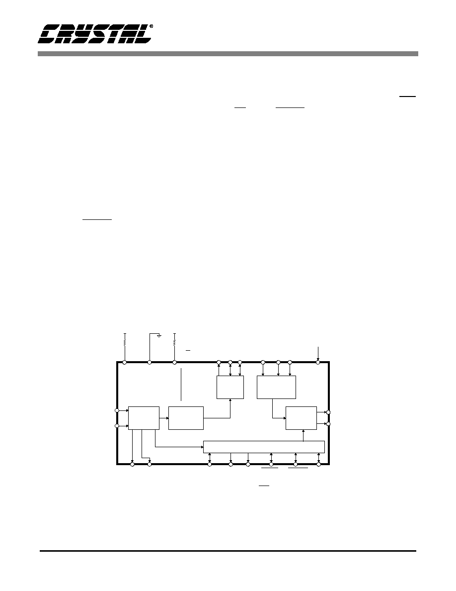
CS8420
56
DS245PP2
14.4
Hardware Mode 3 Description
(Transceive Data Flow, with SRC)
Hardware Mode 3 data flow is shown in Figure 28.
Audio data is input via the AES3 receiver, and rate
converted. The audio data at the new rate is then
output via the serial audio output port. Different au-
dio data, synchronous to OMCK, may be input into
the serial audio input port, and output via the AES3
transmitter.
The channel status data, user data and validity bit
information are handled in 2 alternative modes: 3A
and 3B, determined by a start-up resistor on the
COPY pin. In mode 3A, the received PRO, COPY,
ORIG, and AUDIO channel status bits are output
on pins. The transmitted channel status bits are
copied from the received channel status data, and
the transmitted U and V bits are 0.
In mode 3B, only the COPY and ORIG pins are
output, and reflect the received channel status data.
The transmitted channel status bits, user data and
validity bits are input serially via the PRO/C, EM-
PH/U and AUDIO/V pins. Figure 22 shows the
timing requirements.
The serial audio input port is always a slave.
If a validity, parity, bi-phase or lock receiver error
occurs, the current audio sample will be held.
Start-up options are shown in Table 10, and allow
choice of the serial audio output port as a master or
slave, whether TCBL is an input or an output, the
serial audio ports formats and the source of the
transmitted C, U and V data.
The following pages contain the detailed pin de-
scriptions for hardware mode 3.
AES3
Encoder
& Tx
Serial
Audio
Output
AES3 Rx
&
Decoder
Sample
Rate
Converter
C & U bit Data Buffer
Clocked by
Output Clock
Clocked by
Input Derived Clock
RXP
RXN
OLRCK
OSCLK
SDOUT
TXP
TXN
RMCK RERR
COPY ORIG EMPH/U AUDIO/V TCBL
DFC0
DFC1
VD+
H/S
Output
Clock
Source
OMCK
Power supply pins (VD+, VA+, DGND, AGND) & the reset pin (RST) and the PLL filter pin (FILT)
are omitted from this diagram. Please refer to the Typical Connection Diagram for hook-up details.
VD+
Serial
Audio
Input
ILRCK
ISCLK
SDIN
PRO/C
Figure 28. Hardware Mode 3 - Transceive Data Flow, with SRC

CS8420
DS245PP2
57
SDOUT RMCK RERR ORIG COPY
Function
LO
-
-
-
-
Serial Output Port is Slave
HI
-
-
-
-
Serial Output Port is Master
-
-
-
-
LO
Mode 3A: C transmitted data is copied from received data, U & V =0,
received PRO, EMPH, AUDIO is visible
-
-
-
-
HI
Mode 3B: CUV transmitted data is input serially on pins, received PRO,
EMPH and AUDIO is not visible
-
LO
LO
-
-
Serial Input & Output Format IF1&OF1
-
LO
HI
-
-
Serial Input & Output Format IF2&OF2
-
HI
LO
-
-
Serial Input & Output Format IF3&OF3
-
HI
HI
-
-
Serial Input & Output Format IF2&OF4
-
-
-
LO
-
TCBL is an input
-
-
-
HI
-
TCBL is an output
Table 10. Hardware Mode 3 Start-up Options

CS8420
58
DS245PP2
14.4.1
Pin Description - Hardware Mode 3
Overall Device Control:
DFC0, DFC1 - Data Flow Control Inputs
DFC0 and DFC1 inputs determine the major data flow options available in hardware mode, according to
Table 3.
OMCK - Output Section Master Clock Input
Output section master clock input. The frequency must be 256x the output sample rate (Fso).
Audio Input Interface:
SDIN - Serial Audio Input Port Data Input
Audio data serial input pin. This data will be transmitted out the AES3 port.
ISCLK - Serial Audio Input Port Bit Clock Input
Serial bit clock for audio data on the SDIN pin.
ILRCK - Serial Audio Input Port Left/Right Clock Input
Word rate clock for the audio data on the SDIN pin. The frequency will be at the output sample rate
(Fso)
Audio Output Interface:
SDOUT - Serial Audio Output Port Data Output
Audio data serial output pin. This is also a start-up option pin, and requires a pull-up or pull-down
resistor.
OSCLK - Serial Audio Output Port Bit Clock Input or Output
Serial bit clock for audio data on the SDOUT pin.
OLRCK - Serial Audio Output Port Left/Right Clock Input or Output
Word rate clock for the audio data on the SDOUT pin. The frequency will be at the output sample rate
(Fso).

CS8420
DS245PP2
59
AES3/SPDIF Transmitter Interface:
TXN, TXP - Differential Line Driver Outputs
Differential line driver outputs, transmitting AES3 type data. Drivers are pulled to low while the CS8420
is in the reset state.
TCBL - Transmit Channel Status Block Start
When operated as output, TCBL is high during the first sub-frame of a transmitted channel status block,
and low at all other times. When operated as input, driving TCBL high for at least three OMCK clocks
will cause the current transmitted sub-frame to be the start of a channel status block.
AES3/SPDIF Receiver Interface:
RXP, RXN - Differential Line Receiver Inputs
Differential line receiver inputs, carrying AES3 type data.
RMCK - Input Section Recovered Master Clock Output
Input section recovered master clock output. Will be at a frequency of 256x the input sample rate (Fsi).
This is also a start-up option pin, and requires a pull-up or pull-down resistor.
RERR - Receiver Error Indicator Output
When high, indicates a problem with the operation of the AES3 receiver. The status of this pin is
updated once per sub-frame of incoming AES3 data. Conditions that cause RERR to go high are: parity
error, and bi-phase coding error, as well as loss of lock in the PLL. This is also a start-up option pin,
and requires a pull-up or pull-down resistor.
EMPH/U - Pre-emphasis Indicator Output or U-bit Data Input
The EMPH/U pin either reflects the state of the EMPH channel status bits in the incoming AES3 type
data stream, or is the serial U-bit input for the AES3 type transmitted data, clocked by OLRCK. If
indicating emphasis EMPH/U is low when the incoming data indicates 50/15
µ
s pre-emphasis and high
otherwise.
COPY - Copy Channel Status bit Output
The COPY pin reflects the state of the COPY Channel Status bit in the incoming AES3 type data
stream. This is also a start-up option pin, and requires a pull-up or pull-down resistor.
ORIG - Original Channel Status Output
SCMS generation indicator. This is decoded from the incoming category code and the L bit. A low
output indicates that the audio data stream is 1st generation or higher. A high indicates that the audio
data stream is original. This is also a start-up option pin, and requires a pull-up or pull-down resistor.
PRO/C - Professional Channel Status bit Output or C-bit Data Input
The PRO/C pin either reflects the state of the Professional/Consumer Channel Status bit in the incoming
AES3 type data stream, or is the serial C-bit input for the AES3 type transmitted data, clocked by
OLRCK.
AUDIO/V - Audio Channel Status bit Output or V-bit Data Input
The AUDIO/V pin either reflects the state of the audio/non audio Channel Status bit in the incoming
AES3 type data stream, or is the V-bit data input for the AES3 type transmitted data stream, clocked by
OLRCK.

CS8420
60
DS245PP2
14.5
Hardware Mode 4 Description
(Transceive Data Flow, No SRC)
Hardware Mode 4 data flow is shown in Figure 29.
Audio data is input via the AES3 receiver, and rout-
ed to the serial audio output port. Different audio
data synchronous to RMCK may be input into the
serial audio input port, and output via the AES3
transmitter.
The channel status data, user data and validity bit
information are handled in 2 alternative modes: 4A
and 4B, determined by a start-up resistor on the
COPY pin. In mode 4A, the received PRO, COPY,
ORIG, EMPH, and AUDIO channel status bits are
output on pins. The transmitted channel status bits
are copied from the received channel status data,
and the transmitted U and V bits are 0.
In mode 4B, only the COPY and ORIG pins are
output, and reflect the received channel status data.
The transmitted channel status bits, user data and
validity bits are input serially via the PRO/C, EM-
PH/U and AUDIO/V pins. Figure 22 shows the
timing requirements.
The APMS pin allows the serial audio input port to
be set to master or slave.
If a validity, parity, bi-phase or lock receiver error
occurs, the current audio sample is passed unmod-
ified to the serial audio output port.
Start-up options are shown in Table 11, and allow
choice of the serial audio output port as a master or
slave, whether TCBL is an input or an output, and
the audio serial ports formats and the source of the
transmitted C, U and V data.
The following pages contain the detailed pin de-
scriptions for hardware mode 4.
AES3
Encoder
& Tx
Serial
Audio
Output
AES3 Rx
&
Decoder
C & U bit Data Buffer
RXP
RXN
OLRCK
OSCLK
SDOUT
TXP
TXN
RMCK
RERR
COPY ORIG EMPH/U AUDIO/V
TCBL
DFC0
DFC1
VD+
H/S
Power supply pins (VD+, VA+, DGND, AGND) & the reset pin (RST) and the PLL filter pin (FILT)
are omitted from this diagram. Please refer to the Typical Connection Diagram for hook-up details.
VD+
Serial
Audio
Input
ILRCK
ISCLK
SDIN
PRO/C
APMS
Figure 29. Hardware Mode 4 - Transceive Data Flow, without SRC
CS8420
DS245PP2
61
SDOUT RMCK RERR ORIG COPY
Function
LO
-
-
-
-
Serial Output Port is Slave
HI
-
-
-
-
Serial Output Port is Master
-
-
-
-
LO
Mode 4A: C transmitted data is copied from received data, U & V =0, received
PRO, EMPH, AUDIO is visible
-
-
-
-
HI
Mode 4B: CUV transmitted data is input serially on pins, received PRO,
EMPH and AUDIO is not visible
-
LO
LO
-
-
Serial Input & Output Format IF1&OF1
-
LO
HI
-
-
Serial Input & Output Format IF2&OF2
-
HI
LO
-
-
Serial Input & Output Format IF3&OF3
-
HI
HI
-
-
Serial Input & Output Format IF1&OF5
-
-
-
LO
-
TCBL is an input
-
-
-
HI
-
TCBL is an output
Table 11. Hardware Mode 4 Start-up Options

CS8420
62
DS245PP2
14.5.1
Pin Description - Hardware Mode 4
Overall Device Control:
DFC0, DFC1 - Data Flow Control Inputs
DFC0 and DFC1 inputs determine the major data flow options available in hardware mode, according to
Table 3.
Audio Input Interface:
SDIN - Serial Audio Input Port Data Input
Audio data serial input pin. This data will be transmitted out the AES3 port.
ISCLK - Serial Audio Input Port Bit Clock Input or Output
Serial bit clock for audio data on the SDIN pin.
ILRCK - Serial Audio Input Port Left/Right Clock Input or Output
Word rate clock for the audio data on the SDIN pin. The frequency will be at the input sample rate (Fsi)
APMS - Serial Audio Input Port Master or Slave
APMS should be connected to VD+ to set serial audio input port as a master, or connected to DGND to
set the port as a slave.
Audio Output Interface:
SDOUT - Serial Audio Output Port Data Output
Audio data serial output pin. This is also a start-up option pin, and requires a pull-up or pull-down
resistor.
OSCLK - Serial Audio Output Port Bit Clock Input or Output
Serial bit clock for audio data on the SDOUT pin.
OLRCK - Serial Audio Output Port Left/Right Clock Input or Output
Word rate clock for the audio data on the SDOUT pin. The frequency will be at the input sample rate
(Fsi).

CS8420
DS245PP2
63
AES3/SPDIF Transmitter Interface:
TXN, TXP - Differential Line Driver Outputs
Differential line driver outputs, transmitting AES3 type data. Drivers are pulled to low while the CS8420
is in the reset state.
TCBL - Transmit Channel Status Block Start
When operated as output, TCBL is high during the first sub-frame of a transmitted channel status block,
and low at all other times. When operated as input, driving TCBL high for at least three RMCK clocks
will cause the current transmitted sub-frame to be the start of a channel status block.
AES3/SPDIF Receiver Interface:
RXP, RXN - Differential Line Receiver Inputs
Differential line receiver inputs, carrying AES3 type data.
RMCK - Input Section Recovered Master Clock Output
Input section recovered master clock output. Will be at a frequency of 256x the input sample rate (Fsi).
This is also a start-up option pin, and requires a pull-up or pull-down resistor.
RERR - Receiver Error Indicator Output
When high, indicates a problem with the operation of the AES3 receiver. The status of this pin is
updated once per sub-frame of incoming AES3 data. Conditions that cause RERR to go high are: parity
error, and bi-phase coding error, as well as loss of lock in the PLL. This is also a start-up option pin,
and requires a pull-up or pull-down resistor.
EMPH/U - Pre-emphasis Indicator Output or U-bit Data Input
The EMPH/U pin either reflects the state of the EMPH channel status bit in the incoming AES3 type
data stream, or is the serial U-bit input for the AES3 type transmitted data, clocked by OLRCK. If
indicating emphasis EMPH/U is high when the incoming data indicates 50/15
µ
s pre-emphasis and low
otherwise.
COPY - Copy Channel Status bit Output
The COPY pin reflects the state of the COPY Channel Status bit in the incoming AES3 type data
stream. This is also a start-up option pin, and requires a pull-up or pull-down resistor.
ORIG - Original Channel Status Output
SCMS generation indicator. This is decoded from the incoming category code and the L bit. A low
output indicates that the audio data stream is 1st generation or higher. A high indicates that the audio
data stream is original. This is also a start-up option pin, and requires a pull-up or pull-down resistor.
PRO/C - Professional Channel Status bit Output or C-bit Data Input
The PRO/C pin either reflects the state of the Professional/Consumer Channel Status bit in the incoming
AES3 type data stream, or is the serial C-bit input for the AES3 type transmitted data, clocked by
OLRCK.
AUDIO/V - Audio Channel Status bit Output or V-bit Data Input
The AUDIO/V pin either reflects the state of the audio/non audio Channel Status bit in the incoming
AES3 type data stream, or is the V-bit data input for the AES3 type transmitted data stream, clocked by
OLRCK.
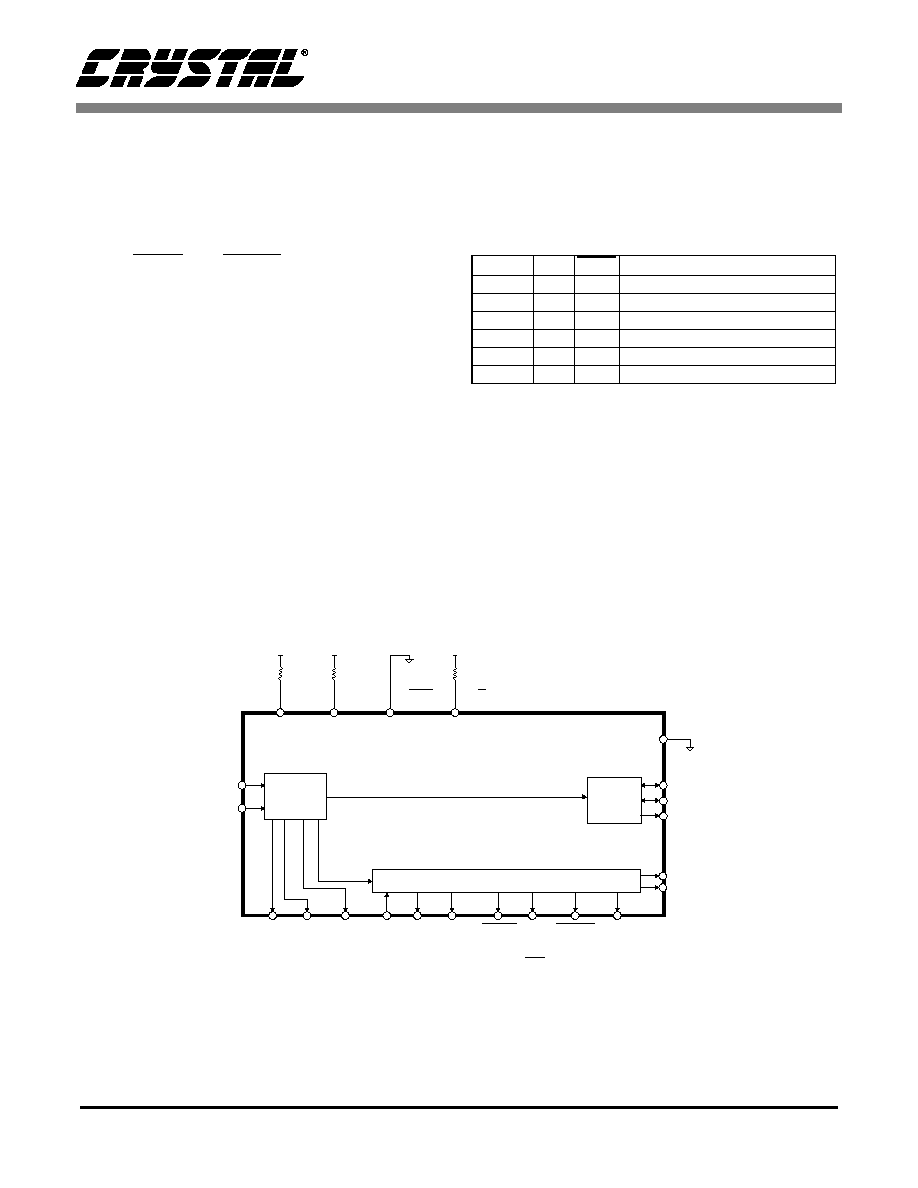
CS8420
64
DS245PP2
14.6
Hardware Mode 5 Description
(AES3 Receiver Only)
Hardware Mode 5 data flow is shown in Figure 30.
Audio data is input via the AES3 receiver, and rout-
ed to the serial audio output port. The PRO, COPY,
ORIG, EMPH, and AUDIO channel status bits are
output on pins. The decoded C and U bits are also
output, clocked by both edges of OLRCK (master
mode only, see Figure 21).
If a validity, parity, bi-phase or lock receiver error
occurs, the current audio sample is passed unmod-
ified to the serial audio output port.
Start-up options are shown in Table 12, and allow
choice of the serial audio output port as a master or
slave, and the serial audio port format. The follow-
ing pages contain the detailed pin descriptions for
hardware mode 5.
Serial
Audio
Output
AES3 Rx
&
Decoder
C & U bit Data Buffer
RXP
RXN
OLRCK
OSCLK
SDOUT
RMCK
RERR
COPY ORIG
EMPH
RCBL
PRO AUDIO
CHS
DFC0
DFC1
S/AES
VD+
H/S
Power supply pins (VD+, VA+, DGND, AGND) & the reset pin (RST) and the PLL filter pin (FILT)
are omitted from this diagram. Please refer to the Typical Connection Diagram for hook-up details.
VD+
VD+
NVERR
C
U
OMCK
Figure 30. Hardware Mode 5 - AES3 Receiver Only
SDOUT ORIG EMPH
Function
LO
-
-
Serial Output Port is Slave
HI
-
-
Serial Output Port is Master
-
LO
LO
Serial Output Format OF1
-
LO
HI
Serial Output Format OF2
-
HI
LO
Serial Output Format OF3
-
HI
HI
Serial Output Format OF5
Table 12. Hardware Mode 5 Start-up Options
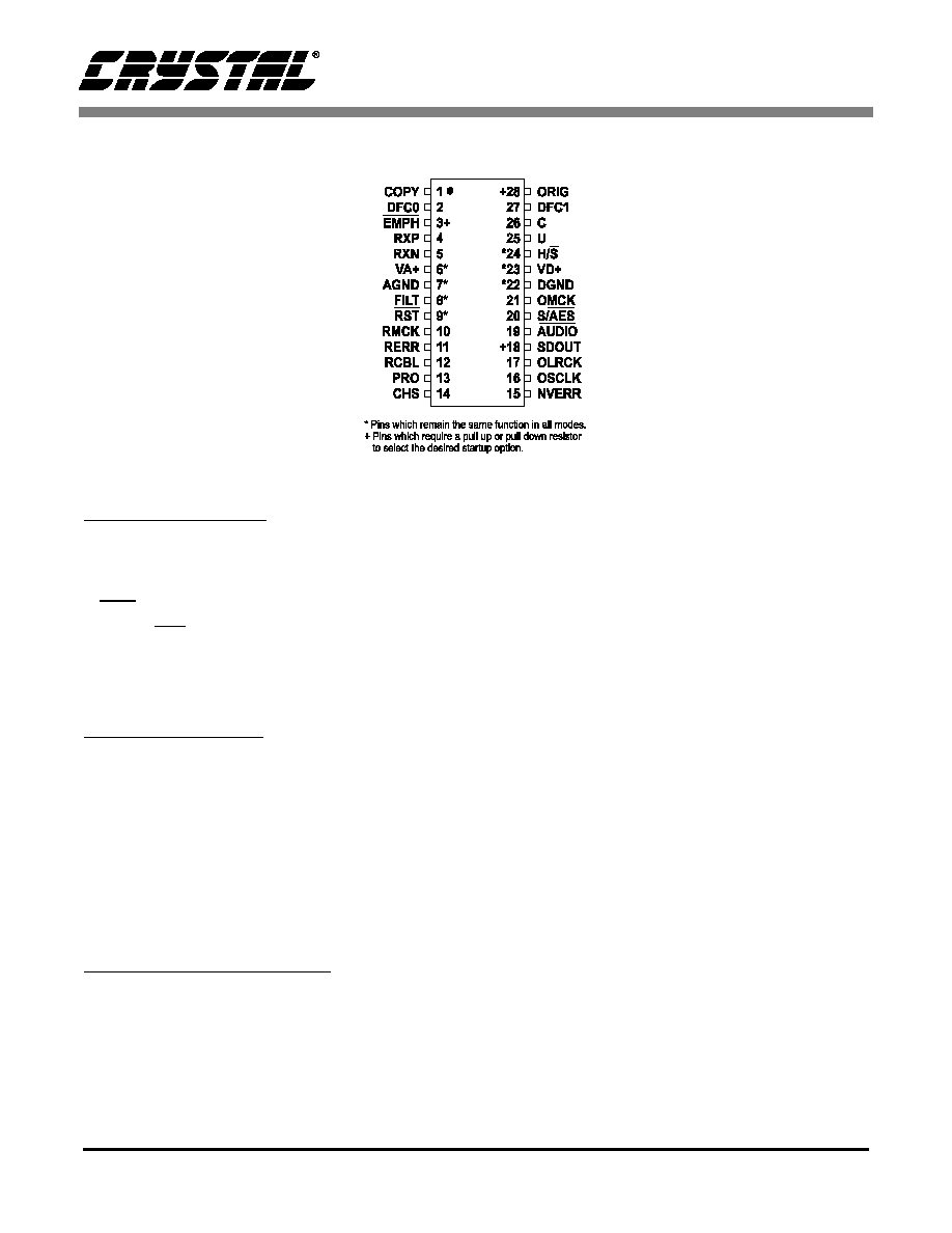
CS8420
DS245PP2
65
14.6.1
Pin Description - Hardware Mode 5
Overall Device Control:
DFC0, DFC1 - Data Flow Control Inputs
DFC0 and DFC1 inputs determine the major data flow options available in hardware mode, according to
Table 3.
S/AES - Serial Audio or AES3 Input Select
S/AES is connected to DGND in hardware mode 5, in order to select the AES3 input.
OMCK - Output Section Master Clock Input
Output section master clock input. This pin is not used in this mode and should be connected to DGND.
Audio Output Interface:
SDOUT - Serial Audio Output Port Data Output
Audio data serial output pin. This is also a start-up option pin, and requires a pull-up or pull-down
resistor.
OSCLK - Serial Audio Output Port Bit Clock Input or Output
Serial bit clock for audio data on the SDOUT pin.
OLRCK - Serial Audio Output Port Left/Right Clock Input or Output
Word rate clock for the audio data on the SDOUT pin. The frequency will be at the input sample rate
(Fsi).
AES3/SPDIF Receiver Interface:
RXP, RXN - Differential Line Receiver Inputs
Differential line receiver inputs, carrying AES3 type data.
RMCK - Input Section Recovered Master Clock Output
Input section recovered master clock output. Will be at a frequency of 256x the input sample rate (Fsi).

CS8420
66
DS245PP2
RERR - Receiver Error Indicator
When high, indicates a problem with the operation of the AES3 receiver. The status of this pin is
updated once per sub-frame of incoming AES3 data. Conditions that cause RERR to go high are:
validity, parity error, and bi-phase coding error, as well as loss of lock in the PLL.
NVERR - No Validity Receiver Error Indicator
When high, indicates a problem with the operation of the AES3 receiver. The status of this pin is
updated once per frame of incoming AES3 data. Conditions that cause NVERR to go high are: parity
error, and bi-phase coding error, as well as loss of lock in the PLL.
EMPH - Pre-emphasis Indicator Output
EMPH is low when the incoming AES3 data indicates the presence of 50/15
µ
s pre-emphasis. When
the AES3 data indicates the absence of pre-emphasis or the presence of non 50/15
µ
s pre-emphasis
EMPH is high. This is also a start-up option pin, and requires a pull-up or pull-down resistor.
COPY - Copy Channel Status bit Output
The COPY pin reflects the state of the COPY Channel Status bit in the incoming AES3 type data
stream.
ORIG - Original Channel Status Output
SCMS generation indicator. This is decoded from the incoming category code and the L bit. A low
output indicates that the audio data stream is 1st generation or higher. A high indicates that the audio
data stream is original. This is also a start-up option pin, and requires a pull-up or pull-down resistor.
PRO - Professional Channel Status bit Output
The PRO pin reflects the state of the Professional/Consumer Channel Status bit in the incoming AES3
type data stream.
AUDIO - Audio Channel Status bit Output
The AUDIO pin reflects the state of the audio/non audio Channel Status bit in the incoming AES3 type
data stream.
RCBL - Receiver Channel Status Block Output
RCBL indicates the beginning of a received channel status block. RCBL goes high 2 frames after the
reception of a Z preamble, remains high for 16 frames while COPY, ORIG, AUDIO, EMPH and PRO are
updated, and returns low for the remainder of the block. RCBL changes on rising edges of RMCK.
CHS - Channel Select Input
Selects which sub-frame's channel status data is output on the EMPH, COPY, ORIG, PRO and AUDIO
pins. Channel A is selected when CHS is low, channel B is selected when CHS is high.
U - User Data Output
The U pin outputs user data from the AES3 receiver, clocked by rising and falling edges of OLRCK.
C - Channel Status Data Output
The C pin outputs channel status data from the AES3 receiver, clocked by rising and falling edges of
OLRCK.
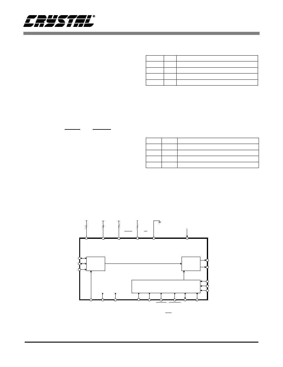
CS8420
DS245PP2
67
14.7
Hardware Mode 6 Description
(AES3 Transmitter Only)
Hardware Mode 6 data flow is shown in Figure 31.
Audio data is input via the serial audio input port
and routed to the AES3 transmitter.
The transmitted channel status, user and validity
data may be input in 2 alternative methods, deter-
mined by the state of the CEN pin. Mode 6A is se-
lected when the CEN pin is low. In mode 6A, the
user data and validity bit are input via the U and V
pins, clocked by both edges of ILRCK. The chan-
nel status data is derived from the state of the
COPY/C, ORIG, EMPH, and AUDIO pins. Table
13 shows how the COPY/C and ORIG pins map to
channel status bits. In consumer mode, the trans-
mitted category code shall be set to Sample Rate
Converter (0101100).
Mode 6B is selected when the CEN pin is high. In
mode 6B, the channel status, user data and validity
bit are input serially via the COPY/C, U and V pins.
These pins are clocked by both edges of ILRCK (if
the port is in master mode). Figure 22 shows the
timing requirements.
The channel status block pin (TCBL) may be an in-
put or an output, determined by the state of the
TCBLD pin. The serial audio input port data format
is selected as shown in Table 14, and may be set to
master or slave by the state of the APMS input pin.
The following pages contain the detailed pin de-
scriptions for hardware mode 6.
AES3
Encoder
& Tx
Serial
Audio
Input
C, U, V Data Buffer
ILRCK
ISCLK
TXP
COPY/C ORIG EMPH AUDIO TCBL
DFC0
DFC1
S/AES
VD+
H/S
Output
Clock
Source
OMCK
Power supply pins (VD+, VA+, DGND, AGND) & the reset pin (RST)
are omitted from this diagram. Please refer to the Typical Connection Diagram for hook-up details.
VD+
SDIN
SFMT1 SFMT0
VD+
FILT
TXN
CEN
U
V
VD+
TCBLD
APMS
Figure 31. Hardware Mode 6 - AES3 Transmitter Only
COPY/C ORIG
Function
0
0
PRO=0, COPY=0, L=0
0
1
PRO=0, COPY=0, L=1
1
0
PRO=0, COPY=1, L=0
1
1
PRO=1
Table 13. HW 6C COPY/C and ORIG pin function
SFMT1 SFMT0
Function
0
0
Serial Input Format IF1
0
1
Serial Input Format IF2
1
0
Serial Input Format IF3
1
1
Serial Input Format IF4
Table 14. HW 6 Serial Audio Port Format Selection

CS8420
68
DS245PP2
14.7.1
Pin Description - Hardware Mode 6
Overall Device Control:
DFC0, DFC1 - Data Flow Control Inputs
DFC0 and DFC1 inputs determine the major data flow options available in hardware mode, according to
Table 3.
S/AES - Serial Audio or AES3 Input Select
S/AES is connected to VD+ in hardware mode 6, in order to select the serial audio input.
SFMT0, SFMT1 - Serial Audio Input Port Data Format Select Inputs
SFMT0 and SFMT1 select the serial audio input port format. See Table 14.
OMCK - Output Section Master Clock Input
Output section master clock input. The frequency must be 256x the output sample rate (Fso).
Audio Input Interface:
SDIN - Serial Audio Input Port Data Input
Audio data serial input pin.
ISCLK - Serial Audio Input Port Bit Clock Input or Output
Serial bit clock for audio data on the SDIN pin.
ILRCK - Serial Audio Input Port Left/Right Clock Input or Output
Word rate clock for the audio data on the SDIN pin.
APMS - Serial Audio Input Port Master or Slave
APMS should be connected to VD+ to set serial audio input port as a master, or connected to DGND to
set the port as a slave.
AES3/SPDIF Transmitter Interface:
TXN, TXP - Differential Line Driver Outputs
Differential line driver outputs, transmitting AES3 type data. Drivers are pulled to low while the CS8420
is in the reset state.
* Pins which remain the same function in all modes.
COPY/C
DFC0
EMPH
SFMT0
SFMT1
VA+
AGND
FILT
RST
APMS
TCBLD
ILRCK
ISCLK
SDIN
28
27
26
25
*24
*23
*22
21
20
19
18
17
16
15
1
2
3
4
5
6*
7*
8*
9*
10
11
12
13
14
ORIG
DFC1
TXP
TXN
H/S
VD+
DGND
OMCK
S/AES
AUDIO
U
V
CEN
TCBL

CS8420
DS245PP2
69
TCBL - Transmit Channel Status Block Start
When operated as output, TCBL is high during the first sub-frame of a transmitted channel status block,
and low at all other times. When operated as input, driving TCBL high for at least three OMCK clocks
will cause the current transmitted sub-frame to be the start of a channel status block.
TCBLD - Transmit Channel Status Block Direction Input
Connect TCBLD to VD+ to set TCBL as an output. Connect TCBLD to DGND to set TCBL as an input.
EMPH - Pre-emphasis Indicator Input
In mode 6B, EMPH pin low sets the 3 EMPH channel status bits to indicate 50/15
µ
s pre-emphasis. If
EMPH is high the 3 EMPH channel status bits are set to 000 indicating no pre-emphasis.
COPY/C - COPY Channel Status bit Input or C bit Input
In mode 6B, the COPY/C pin determines the state of the COPY, PRO and L Channel Status bits in the
outgoing AES3 type data stream (See Table 13). In mode 6A, the COPY/C pin becomes the direct C bit
input data pin.
ORIG - ORIG Channel Status bit Input
In mode 6B, the ORIG pin determines the state of the COPY, PRO and L Channel Status bits in the
outgoing AES3 type data stream. See Table 13.
AUDIO - Audio Channel Status bit Input
In mode 6B, the AUDIO pin determines the state of the audio/non audio Channel Status bit in the
outgoing AES3 type data stream.
V - Validity bit Input
In modes 6A and 6B, the V pin input determines the state of the validity bit in the outgoing AES3
transmitted data. This pin is sampled on both edges of the ILRCK.
U - User Data bit Input
In modes 6A and 6B, the U pin input determines the state of the user data bit in the outgoing AES3
transmitted data. This pin is sampled on both edges of the ILRCK.
CEN - C bit Input Enable Mode Input
The CEN pin determines how the channel status data bits are input. When CEN is low, hardware mode
6A is selected, where the COPY/C, ORIG, EMPH and AUDIO pins are used to enter selected channel
status data. When CEN is high, hardware mode 6B is selected, where the COPY/C pin is used to enter
serial channel status data.

CS8420
70
DS245PP2
15. APPENDIX A: EXTERNAL
AES3/SPDIF/IEC60958
TRANSMITTER AND RECEIVER
COMPONENTS
This section details the external components re-
quired to interface the AES3 transmitter and re-
ceiver to cables and fiber-optic components.
15.1
AES3 Transmitter External
Components
The output drivers on the CS8420 are designed to
drive both the professional and consumer interfac-
es. The AES3 specification for professional/broad-
cast use calls for a 110
source impedance and a
balanced drive capability. Since the transmitter
output impedance is very low, a 110
resistor
should be placed in series with one of the transmit
pins. The specifications call for a balanced output
drive of 2-7 volts peak-to-peak into a 110
load
with no cable attached. Using the circuit in
Figure 32, the output of the transformer is short-
circuit protected, has the proper source impedance,
and provides a 5 volt peak-to-peak signal into a
110
load. Lastly, the two output pins should be
attached to an XLR connector with male pins and a
female shell, and with pin 1 of the connector
grounded.
In the case of consumer use, the IEC60958 specifi-
cations call for an unbalanced drive circuit with an
output impedance of 75
and a output drive level
of 0.5 V peak-to-peak ±20% when measured across
a 75
load using no cable. The circuit shown in
Figure 33 only uses the TXP pin and provides the
proper output impedance and drive level using
standard 1% resistors. The connector for a consum-
er application would be an RCA phono socket. This
circuit is also short circuit protected.
The TXP pin may be used to drive TTL or CMOS
gates as shown in Figure 34. This circuit may be
used for optical connectors for digital audio since
they usually have TTL or CMOS compatible in-
puts. This circuit is also useful when driving multi-
ple digital audio outputs since RS422 line drivers
have TTL compatible inputs.
15.2
AES3 Receiver External Components
The CS8420 AES3 receiver is designed to accept
both the professional and consumer interfaces. The
digital audio specifications for professional use call
for a balanced receiver, using XLR connectors,
with 110
±20% impedance. The XLR connector
on the receiver should have female pins with a male
shell. Since the receiver has a very high input im-
pedance, a 110
resistor should be placed across
the receiver terminals to match the line impedance,
as shown in Figure 35. Although transformers are
not required by the AES, they are, however, strong-
ly recommended.
If some isolation is desired without the use of trans-
formers, a 0.01
µ
F capacitor should be placed in se-
110
TXP
TXN
XLR
1
CS8420
Figure 32. Professional Output Circuit
374
90.9
TXP
TXN
RCA
Phono
CS8420
Figure 33. Consumer Output Circuit
TXP
TXN
TTL or
CMOS Gate
CS8420
Figure 34. TTL/CMOS Output Circuit

CS8420
DS245PP2
71
ries with each input pin (RXP and RXN) as shown
in Figure 36. However, if a transformer is not used,
high frequency energy could be coupled into the re-
ceiver, causing degradation in analog performance.
Figures 35 and 36 show an optional DC blocking
capacitor (0.1
µ
F to 0.47
µ
F) in series with the ca-
ble input. This improves the robustness of the re-
ceiver, preventing the saturation of the transformer,
or any DC current flow, if a DC voltage is present
on the cable.
In the configuration of systems, it is important to
avoid ground loops and DC current flowing down
the shield of the cable that could result when boxes
with different ground potentials are connected.
Generally, it is good practice to ground the shield
to the chassis of the transmitting unit, and connect
the shield through a capacitor to chassis ground at
the receiver. However, in some cases it is advanta-
geous to have the ground of two boxes held to the
same potential, and the cable shield might be de-
pended upon to make that electrical connection.
Generally, it may be a good idea to provide the op-
tion of grounding or capacitively coupling the
shield to the chassis.
In the case of the consumer interface, the standards
call for an unbalanced circuit having a receiver im-
pedance of 75
±5%. The connector for the con-
sumer interface is an RCA phono socket. The
receiver circuit for the consumer interface is shown
in Figure 37.
The circuit shown in Figure 38 may be used when
external RS422 receivers, optical receivers or other
TTL/CMOS logic outputs drive the CS8420 receiv-
er section.
15.3
Isolating Transformer Requirements
The transformer should be capable of operating
from 1.5 to 14 MHz, which is equivalent to an au-
dio data rate of 25 kHz to 108 kHz after bi-phase
mark encoding. Transformers provide isolation
from ground loops, 60Hz noise, and common mode
noise and interference. One of the important con-
siderations when choosing transformers is mini-
mizing shunt capacitance between primary and
secondary windings. The higher the shunt capaci-
tance, the lower the isolation between primary and
secondary, and the more coupling of high frequen-
cy energy. This energy appears in the form of com-
mon mode noise on the receive side ground and has
the potential to degrade analog performance.
Therefore, for best performance, shielded trans-
formers optimized for minimum shunt capacitance
should be used. See Application Note 134 for a se-
lection of manufacturers and their part numbers.
1
XLR
Twisted
Pair
110
110
CS8420
RXP
RXN
* See Text
Figure 35. Professional Input Circuit
1
XLR
Twisted
Pair
110
110
CS8420
RXP
RXN
0.01 F
µ
0.01 F
µ
* See Text
Figure 36. Transformerless Professional Input Circuit
RCA Phono
RXP
RXN
CS8420
Coax
75
75
0.01 F
µ
0.01 F
µ
Figure 37. Consumer Input Circuit
RXP
RXN
CS8420
0.01 F
µ
0.01 F
µ
TTL/CMOS
Gate
Figure 38. TTL/CMOS Input Circuit
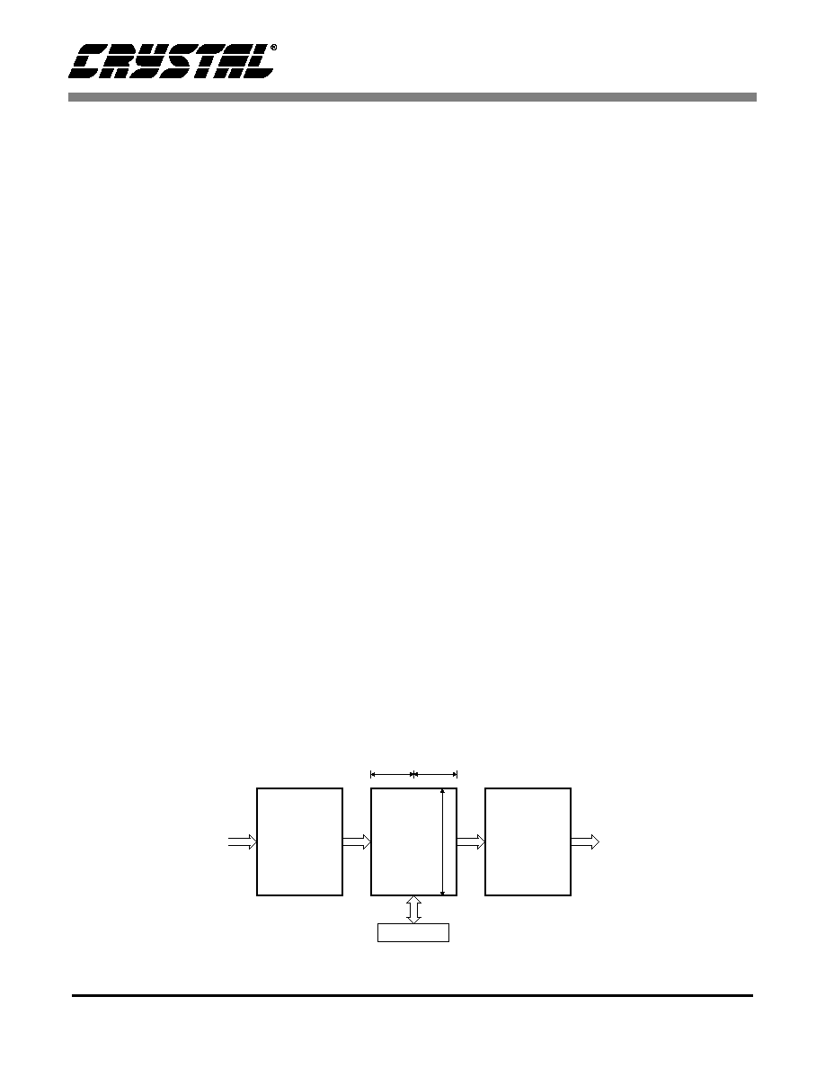
CS8420
72
DS245PP2
16. APPENDIX B: CHANNEL STATUS
AND USER DATA BUFFER
MANAGEMENT
The CS8420 has a comprehensive channel status
(C) and user (U) data buffering scheme, which al-
lows automatic management of channel status
blocks and user data. Alternatively, sufficient con-
trol and access is provided to allow the user to com-
pletely manage the C and U data via the control
port.
16.1
AES3 Channel Status(C) Bit
Management
The CS8420 contains sufficient RAM to store a full
block of C data for both A and B channels (192x2
= 384 bits), and also 384 bits of U information. The
user may read from or write to these RAMs via the
control port.
Unlike the audio data, it is not possible to 'sample-
rate' convert the C bits. This is because specific
meanings are associated with fixed-length data pat-
terns, which should not be altered. Since the output
data rate of the CS8420 will differ from the input
rate when sample-rate conversion is done, it is not
feasible to directly transfer incoming C data to the
output. The CS8420 manages the flow of channel
status data at the block level, meaning that entire
blocks of channel status information are buffered at
the input, synchronized to the output timebase, and
then transmitted. The buffering scheme involves a
cascade of 3 block-sized buffers, named D,E and F,
as shown in Figure 39. The MSB of each byte rep-
resents the first bit in the serial C data stream. For
example, the MSB of byte 0 (which is at control
port address 32) is the consumer/professional bit
for channel status block A.
The first buffer, D, accepts incoming C data from
the AES receiver. The 2nd buffer, E, accepts entire
blocks of data from the D buffer. The E buffer is
also accessible from the control port, allowing read
and writing of the C data. The 3rd buffer (F) is used
as the source of C data for the AES3 transmitter.
The F buffer accepts block transfers from the E
buffer.
If the input rate is slower than the output rate (so
that in a given time interval, more channel status
blocks are transmitted than received), some buff-
ered C blocks will be transmitted multiple times. If
the input rate is faster than the output rate, some
will not be transmitted at all. This is illustrated in
Figure 40). In this manner, channel status block in-
tegrity is maintained. If the transmitted sample
count bits are important in the application, then
they will need to be updated via the control port by
the microcontroller for every outgoing block.
16.1.1
Manually accessing the E buffer
The user can monitor the data being transferred by
reading the E buffer, which is mapped into the reg-
ister space of the CS8420, via the control port. The
user can modify the data to be transmitted by writ-
ing to the E buffer.
Control Port
From
AES3
Receiver
To
AES3
Transmitter
E
24
words
8-bits
8-bits
A
B
D
F
Received
Data
Buffer
Transmit
Data
Buffer
Figure 39. Channel Status Data Buffer Structure

CS8420
DS245PP2
73
The user can configure the interrupt enable register
to cause interrupts to occur whenever "D to E" or
"E to F" buffer transfers occur. This allows deter-
mination of the allowable time periods to interact
with the E buffer.
Also provided are "D to E" and "E to F" inhibit
bits. The associated buffer transfer is disabled
whenever the user sets these bits. These may be
used whenever "long" control port interactions are
occurring. They can also be used to align the be-
havior of the buffers with the selected audio data
flow. For example, if the audio data flow is serial
port in to AES3 out, then it is necessary to inhibit
"D toE" transfers, since these would overwrite the
desired transmit C data with invalid data.
Flowcharts for reading and writing to the E buffer
are shown in Figures 41 and 42. For reading, since
a D to E interrupt just occurred, then there a sub-
stantial time interval until the next D to E transfer
(approximately 192 frames worth of time). This is
usually plenty of time to access the E data without
having to inhibit the next transfer.
For writing, the sequence starts after a E to F trans-
fer, which is based on the output timebase. Since a
D to E transfer could occur at any time (this is
based on the input timebase), then it is important to
inhibit D to E transfers while writing to the E buffer
until all writes are complete. Then wait until the
next E to F transfer occurs before enabling D to E
transfers. This ensures that the data written to the E
buffer actually gets transmitted and not overwritten
by a D to E transfer.
If the channel status block to transmit indicates
PRO mode, then the CRCC byte is automatically
calculated by the CS8420, and does not have to be
written into the last byte of the block by the host
microcontroller.
block 1
block 2
block 3
block 4
block 5
block 1
block 1
block 2
block 3
block 3
block 4
block 5
Contents of E buffer
Updated at Fsi rate
Contents of F buffer
Updated from E
Output at Fso rate
Fso > Fsi (3/2) Causes blocks 1 and 3 to be transmitted twice
Fso < Fsi (2/3) Causes blocks 3 and 6 to not be transmitted
Contents of E buffer
Updated at Fsi rate
Contents of F buffer
Updated from E
Output at Fso rate
block 1
block 2
block 3
block 4
block 5
block 6
block 7
block 1
block 2
block 4
block 5
block 7
Figure 40. Channel Status Block Handling When Fso is Not Equal to Fsi
D to E interrupt occurs
Optionally set D to E inhibit
Read E data
If set, clear D to E inhibit
Return
Figure 41. Flowchart for Reading the E Buffer
E to F interrupt occurs
Optionally set E to F inhibit
Clear D to E inhibit
If set, clear E to F inhibit
Return
Set D to E inhibit
Write E data
Wait for E to F transfer
Figure 42. Flowchart for Writing the E Buffer

CS8420
74
DS245PP2
16.1.2
Reserving the first 5 bytes in the E
buffer
D to E buffer transfers periodically overwrite the
data stored in the E buffer. This can be a problem
for users who want to transmit certain channel sta-
tus settings which are different from the incoming
settings. In this case, the user would have to super-
impose his settings on the E buffer after every D to
E overwrite.
To avoid this problem, the CS8420 has the capabil-
ity of reserving the first 5 bytes of the E buffer for
user writes only. When this capability is in use, in-
ternal D to E buffer transfers will NOT affect the
first 5 bytes of the E buffer. Therefore, the user can
set values in these first 5 E bytes once, and the set-
tings will persist until the next user change. This
mode is enabled via the Channel Status Data Buffer
Control register.
16.1.3
Serial Copy Management System
(SCMS)
In software mode, the CS8420 allows read/modi-
fy/write access to all the channel status bits. For
consumer mode SCMS compliance, the host mi-
crocontroller needs to read and manipulate the Cat-
egory Code, Copy bit and L bit appropriately.
In hardware mode, the SCMS protocol can be fol-
lowed by either using the COPY and ORIG input
pins, or by using the C bit serial input pin. These
options are documented in the hardware mode sec-
tion of this data sheet (starting on14 page 49)
16.1.4
Channel Status Data E Buffer
Access
The E buffer is organized as 24 x 16-bit words. For
each word the MS Byte is the A channel data, and
the LS Byte is the B channel data (see Figure 39).
There are two methods of accessing this memory,
known as one byte mode and two byte mode. The
desired mode is selected via a control register bit.
16.1.5
One Byte mode
In many applications, the channel status blocks for
the A and B channels will be identical. In this situ-
ation, if the user reads a byte from one of the chan-
nel's blocks, the corresponding byte for the other
channel will be the same. Similarly, if the user
wrote a byte to one channel's block, it would be
necessary to write the same byte to the other block.
One byte mode takes advantage of the often identi-
cal nature of A and B channel status data.
When reading data in one byte mode, a single byte
is returned, which can be from channel A or B data,
depending on a register control bit. If a write is be-
ing done, the CS8420 expects a single byte to be in-
put to its control port. This byte will be written to
both the A and B locations in the addressed word.
One byte mode saves the user substantial control
port access time, as it effectively accesses 2 bytes
worth of information in 1 byte's worth of access
time. If the control port's auto-increment address-
ing is used in combination with this mode, multi-
byte accesses such as full-block reads or writes can
be done especially efficiently.
16.1.6
Two Byte mode
There are those applications in which the A and B
channel status blocks will not be the same, and the
user is interested in accessing both blocks. In these
situations, two byte mode should be used to access
the E buffer.
In this mode, a read will cause the CS8420 to out-
put two bytes from its control port. The first byte
out will represent the A channel status data, and the
2nd byte will represent the B channel status data.
Writing is similar, in that two bytes must now be
input to the CS8420's control port. The A channel
status data is first, B channel status data second.

CS8420
DS245PP2
75
16.2
AES3 User (U) Bit Management
The CS8420 U bit manager has four operating
modes:
Mode 1. Transmit all zeros.
Mode 2. Block mode.
Mode 3. Reserved
Mode 4. IEC Consumer B.
16.2.1
Mode 1: Transmit All Zeros
Mode 1 causes only zeros to be transmitted in the
output U data, regardless of E buffer contents or U
data embedded in an input AES3 data stream. This
mode is intended for the user who does not want to
transceive U data, and simply wants the output U
channel to contain no data.
16.2.2
Mode 2: Block Mode
Mode 2 is very similar to the scheme used to con-
trol the C bits. Entire blocks of U data are buffered
from input to output, using a cascade of 3 block-
sized RAMs to perform the buffering. The user has
access to the second of these 3 buffers, denoted the
E buffer, via the control port. Block mode is de-
signed for use in AES3 in, AES3 out situations in
which input U data is decoded using a microcon-
troller via the control port. It is also the only mode
in which the user can merge his own U data into the
transmitted AES3 data stream.
The U buffer access only operates in two byte
mode, since there is no concept of A and B blocks
for user data. The arrangement of the data in the
each byte is that the MSB is the first received bit
and is the first transmitted bit. The first byte read is
the first byte received, and the first byte sent is the
first byte transmitted.
16.2.3
IEC60958 Recommended U Data
Format For Consumer Applications
Modes (3) and (4) are intended for use in AES3 in,
AES3 out situations, in which the input U data is
formatted as recommended in the "IEC60958 Dig-
ital Audio Interface, part 3: Consumer applica-
tions" document.
In this format, "messages" are formed in the U data
from Information Units or IUs. An IU is 8 bits long,
and the MSB is always 1, and is called the start bit,
or 'P' bit. The remaining 7 bits are called Q R S T U
V & W, and carry the desired data.
A "message" consists of 3 to 129 IUs. Multiple IUs
are considered to be in the same message if they are
separated by zero to eight 0s, denoted here as filler.
A filler sequence of nine or more 0s indicates an in-
ter-message gap. The desired information is nor-
mally carried in the sequence of corresponding bits
in the IUs. For example, the sequential Q bits from
each IU make up the Q sub-code data that is used to
indicate Compact Disk track information. This data
is automatically extracted from the received
IEC60958 stream, and is presented in the control
port register map space.
Where incoming U data is coded in the above for-
mat, and needs to be re-transmitted, the data trans-
fer cannot be done using shift registers, because of
the different Fsi and Fso sampling clocks. Instead,
input data must be buffered in a FIFO structure, and
then read out by the AES3 transmitter at appropri-
ate times.
Each bit of each IU must be transceived; unlike the
audio samples, there can be no sample rate conver-
sion of the U data. Therefore, there are 2 potential
problems:
(1) Message Partitioning
When Fso > Fsi, more data is transmitted than re-
ceived per unit time. The FIFO will frequently be
completely emptied. Sensible behavior must occur
when the FIFO is empty, otherwise, a single incom-
ing message may be erroneously be partitioned into
multiple, smaller, messages.
(2) Overwriting
When Fso < Fsi, more data is received than trans-
mitted per unit time. There is a danger of the FIFO

CS8420
76
DS245PP2
becoming completely full, allowing incoming data
to overwrite data that has not yet been output
through the AES3 transmitter.
16.2.4
Mode (3): Reserved
This mode has been removed. Use IEC Consumer
mode B.
16.2.5
Mode (4): IEC Consumer B
In this mode, the partitioning problem is solved by
buffering an entire message before starting to trans-
mit it. In this scheme, zero-segments between mes-
sages will be expanded when Fso > Fsi, but the
integrity of individual messages is preserved.
The overwriting problem (when Fso < Fsi) is
solved by only storing a portion of the input U data
in the FIFO. Specifically, only the IUs themselves
are stored (and not the zeroes that provide inter-IU
and inter-message "filler"). An inter-IU filler seg-
ment of fixed length (OF) will be added back to the
messages at the FIFO output, where the length of
OF is equal to the shortest observed input filler seg-
ment (IF).
Storing only IUs (and not filler) within the FIFO
makes it possible for the slower AES3 transmitter
to "catch up" to the faster AES3 receiver as data is
read out of the FIFO. This is because nothing is
written into the FIFO when long strings of zeroes
are input to the AES-EBU receiver. During this
time of no writing, the transmitter can read out data
that had previously accumulated, allowing the
FIFO to empty out. If the FIFO becomes complete-
ly empty, zeroes are transmitted until a complete
message is written into the FIFO.
Mode 4 is not fail-safe; the FIFO can still get com-
pletely full if there isn't enough "zero-padding" be-
tween incoming messages. It is up to the user to
provide proper padding, as defined below:
Minimum padding
= (Fsi/Fso - 1)*[8N + (N-1)*IF +9] + 9
where N is the number of IUs in the message, IF is
the number of filler bits between each IU, and Fso
Fsi.
Example 1: Fsi/Fso = 2, N=4, IF=1: minimum
proper padding is 53 bits.
Example 2: Fsi/Fso = 1, N=4, IF=7: min proper
padding is 9 bits.
The CS8420 detects when an overwrite has oc-
curred in the FIFO, and synchronously resets the
entire FIFO structure to prevent corrupted U data
from being merged into the transmitted AES3 data
stream. The CS8420 can be configured to generate
an interrupt when this occurs.
Mode 4 is recommended for properly formatted U
data where mode 3 cannot provide acceptable per-
formance, either because of a too-extreme Fsi/Fso
ratio, or because it's unacceptable to change the
lengths of filler segments. Mode 4 provides error-
free performance over the complete range of
Fsi/Fso ratios (provided that the input messages are
properly zero-padded for Fsi > Fso).

CS8420
DS245PP2
77
17. PARAMETER DEFINITIONS
Input Sample Rate (Fsi)
The sample rate of the incoming digital audio.
Input Frame Rate
The frame rate of the received AES3 format data.
Output Sample Rate (Fso)
The sample rate of the outgoing digital audio.
Output Frame Rate
The frame rate of the transmitted AES3 format data.
Dynamic Range
The ratio of the maximum signal level to the noise floor.
Total Harmonic Distortion and Noise
The ratio of the noise and distortion to the test signal level. Normally referenced to 0 dBFS.
Peak Idle Channel Noise Component
With an all-zero input, what is the amplitude of the largest frequency component visible with a 16K point
FFT. The value is in dB ratio to full-scale.
Input Jitter Tolerance
The amplitude of jitter on the AES3 stream, or in the ILRCK clock, that will cause measurable artifacts
in the SRC output. Test signal is full scale 9 kHz, Fsi is 48 kHz, Fso is different 48 kHz, jitter is 2 kHz
sinusoidal, and audio band white noise.
AES3 Transmitter Output Jitter
With a jitter free OMCK clock, what is the jitter added by the AES3 transmitter.
Gain Error
The difference in amplitude between the output and the input signal level, within the passband of the
digital filter in the SRC.
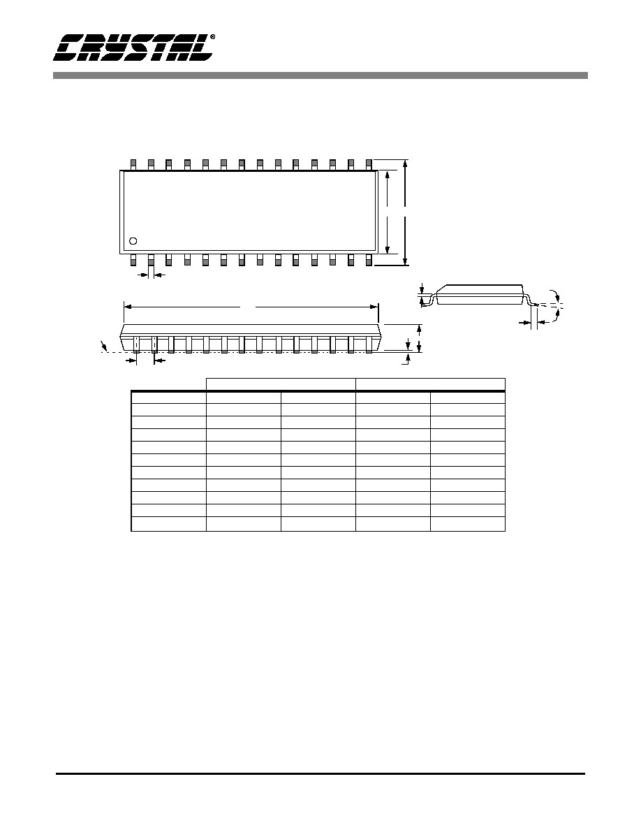
CS8420
78
DS245PP2
18. PACKAGE DIMENSIONS
INCHES
MILLIMETERS
DIM
MIN
MAX
MIN
MAX
A 0.093
0.104
2.35
2.65
A1
0.004
0.012
0.10
0.30
B
0.013
0.020
0.33
0.51
C
0.009
0.013
0.23
0.32
D
0.697
0.713
17.70
18.10
E
0.291
0.299
7.40
7.60
e
0.040
0.060
1.02
1.52
H
0.394
0.419
10.00
10.65
L
0.016
0.050
0.40
1.27
0∞
8∞
0∞
8∞
28L SOIC (300 MIL BODY) PACKAGE DRAWING
D
H
E
b
A1
A
c
L
SEATING
PLANE
1
e

∑ Notes ∑
