Copyright
Cirrus Logic, Inc. 2001
(All Rights Reserved)
CS8900A
Product Data Sheet
&U\VWDO /$1TM ISA Ethernet
Controller
FEATURES
I Single-Chip IEEE 802.3 Ethernet Controller with
Direct ISA-Bus Interface
I Maximum Current Consumption = 55 mA (5V Supply)
I 3 V Operation
I Industrial Temperature Range
I Comprehensive Suite of Software Drivers Available
I Efficient PacketPageTM Architecture Operates in
I/O and Memory Space, and as DMA Slave
I Full Duplex Operation
I On-Chip RAM Buffers Transmit and Receive Frames
I 10BASE-T Port with Analog Filters, Provides:
-- Automatic Polarity Detection and Correction
I AUI Port for 10BASE2, 10BASE5 and 10BASE-F
I Programmable Transmit Features:
-- Automatic Re-transmission on Collision
-- Automatic Padding and CRC Generation
I Programmable Receive Features:
-- Stream TransferTM for Reduced CPU Overhead
-- Auto-Switch Between DMA and On-Chip Memory
-- Early Interrupts for Frame Pre-Processing
-- Automatic Rejection of Erroneous Packets
I EEPROM Support for Jumperless Configuration
I Boot PROM Support for Diskless Systems
I Boundary Scan and Loopback Test
I LED Drivers for Link Status and LAN Activity
I Standby and Suspend Sleep Modes
DESCRIPTION
The CS8900A is a low-cost Ethernet LAN Controller op-
timized for Industry Standard Architecture (ISA)
Personal Computers. Its highly-integrated design elimi-
nates the need for costly external components required
by other Ethernet controllers. The CS8900A includes
on-chip RAM, 10BASE-T transmit and receive filters,
and a direct ISA-Bus interface with 24 mA Drivers.
In addition to high integration, the CS8900A offers a
broad range of performance features and configuration-
options. Its unique PacketPage architecture
automatically adapts to changing network traffic pat-
terns and available system resources. The result is
increased system efficiency.
The CS8900A is available in a 100-pin TQFP package
ideally suited for small form-factor, cost-sensitive Ether-
net applications. With the CS8900A, system engineers
can design a complete Ethernet circuit that occupies
less than 1.5 square inches (10 sq. cm) of board space.
ORDERING INFORMATION
CS8900A-CQ 0� to 70� C 5V TQFP-100
CS8900A-IQ -40� to 85� C 5V TQFP-100
CS8900A-CQ3 0� to 70� C
3.3V TQFP-100
CS8900A-IQ3 -40� to 85� C 3.3V TQFP-100
CRD8900A-1
Evaluation Kit
EEPROM
RJ-45
10BASE-T
Attachment
Unit
Interface
(AUI)
20 MHz
XTAL
RAM
ISA
Bus
Logic
Memory
Manager
802.3
MAC
Engine
EEPROM
Control
Encoder/
Decoder
&
PLL
10BASE-T
RX Filters &
Receiver
10BASE-T
TX Filters &
Transmitter
AUI
Transmitter
AUI
Collision
AUI
Receiver
Clock
Power
Manager
Boundary
Scan
Test Logic
LED
Control
CS8900A ISA Ethernet Controller
I
S
A
DS271PP4
APR `01
CIRRUS LOGIC PRODUCT DATASHEET

2
DS271PP4
CS8900A
Crystal LANTM ISA Ethernet Controller
CIRRUS LOGIC PRODUCT DATASHEET
TABLE OF CONTENTS
1.0 INTRODUCTION ......................................................................................................................7
1.1 General Description ............................................................................................................7
1.1.1 TDirect ISA-Bus Interface ......................................................................................7
1.1.2 TIntegrated Memory ..............................................................................................7
1.1.3 T802.3 Ethernet MAC Engine ................................................................................7
1.1.4 TEEPROM Interface ..............................................................................................7
1.1.5 TComplete Analog Front End ................................................................................7
1.2 System Applications ...........................................................................................................7
1.2.1 TMotherboard LANs ..............................................................................................7
1.2.2 TEthernet Adapter Cards .......................................................................................8
1.3 Key Features and Benefits .................................................................................................9
1.3.1 TVery Low Cost .....................................................................................................9
1.3.2 THigh Performance ................................................................................................9
1.3.3 TLow Power and Low Noise ..................................................................................9
1.3.4 TComplete Support ...............................................................................................9
2.0 PIN DESCRIPTION .............................................................................................................11
3.0 FUNCTIONAL DESCRIPTION ...............................................................................................16
3.1 Overview ..........................................................................................................................16
3.1.1 TConfiguration .....................................................................................................16
3.1.2 TPacket Transmission .........................................................................................16
3.1.3 TPacket Reception ..............................................................................................16
3.2 ISA Bus Interface .............................................................................................................17
3.2.1 TMemory Mode Operation ...................................................................................17
3.2.2 TI/O Mode Operation ...........................................................................................17
3.2.3 TInterrupt Request Signals ..................................................................................17
3.2.4 TDMA Signals ......................................................................................................17
3.3 Reset and Initialization .....................................................................................................18
3.3.1 TReset .................................................................................................................18
3.3.1.1 External Reset, or ISA Reset ...............................................................18
3.3.1.2 Power-Up Reset ..................................................................................18
3.3.1.3 Power-Down Reset ..............................................................................18
3.3.1.4 EEPROM Reset ...................................................................................18
3.3.1.5 Software Initiated Reset .......................................................................18
3.3.1.6 Hardware (HW) Standby or Suspend ..................................................18
3.3.1.7 Sof tware (SW) Suspend .....................................................................18
3.3.2 TAllowing Time for Reset Operation ....................................................................18
3.3.3 TBus Reset Considerations .................................................................................18
3.3.4 TInitialization ........................................................................................................19
3.4 Configurations with EEPROM ..........................................................................................20
3.4.1 TEEPROM Interface ............................................................................................20
3.4.2 TEEPROM Memory Organization ........................................................................20
3.4.3 TReset Configuration Block .................................................................................20
3.4.3.1 Reset Configuration Block Structure ....................................................20
3.4.3.2 Reset Configuration Block Header ......................................................20
3.4.3.3 Determining the EEPROM Type ..........................................................20
3.4.3.4 Checking EEPROM for presence of Reset Configuration Block ..........20
3.4.3.5 Determining Number of Bytes in the Reset Configuration Block .........21
3.4.4 TGroups of Configuration Data ............................................................................21
3.4.4.1 Group Header ......................................................................................22
3.4.5 TReset Configuration Block Checksum ...............................................................22
3.4.6 TEEPROM Example ............................................................................................22
3.4.7 TEEPROM Read-out ...........................................................................................22

DS271PP4
3
CS8900A
Crystal LANTM ISA Ethernet Controller
CIRRUS LOGIC PRODUCT DATASHEET
3.4.7.1 Determining EEPROM Size ................................................................. 22
3.4.7.2 Loading Configuration Data ................................................................. 23
3.4.8 TEEPROM Read-out Completion ........................................................................ 23
3.5 Programming the EEPROM ............................................................................................. 23
3.5.1 TEEPROM Commands ....................................................................................... 23
3.5.2 TEEPROM Command Execution ........................................................................ 23
3.5.3 TEnabling Access to the EEPROM .....................................................................24
3.5.4 TWriting and Erasing the EEPROM .................................................................... 24
3.6 Boot PROM Operation ..................................................................................................... 24
3.6.1 TAccessing the Boot PROM ................................................................................ 24
3.6.2 TConfiguring the CS8900A for Boot PROM Operation ....................................... 24
3.7 Low-Power Modes ..........................................................................................................25
3.7.1 THardware Standby ............................................................................................ 25
3.7.2 THardware Suspend ........................................................................................... 25
3.7.3 TSoftware Suspend ............................................................................................. 26
3.8 LED Outputs ..................................................................................................................... 27
3.8.0.1 LANLED .............................................................................................. 27
3.8.0.2 LINKLED or HC0 ................................................................................. 27
3.8.0.3 BSTATUS or HC1 ............................................................................... 27
3.8.1 TLED Connection ................................................................................................ 27
3.9 Media Access Control ......................................................................................................27
3.9.1 TOverview ........................................................................................................... 27
3.9.2 TFrame Encapsulation and Decapsulation ......................................................... 28
3.9.2.1 Transmission ....................................................................................... 28
3.9.2.2 Reception ............................................................................................ 28
3.9.2.3 Enforcing Minimum Frame Size .......................................................... 28
3.9.3 TTransmit Error Detection and Handling ............................................................. 29
3.9.3.1 Loss of Carrier ..................................................................................... 29
3.9.3.2 SQE Error ............................................................................................ 29
3.9.3.3 Out-of-Window (Late) Collision ............................................................ 29
3.9.3.4 Jabber Error ........................................................................................ 29
3.9.3.5 Transmit Collision ................................................................................ 29
3.9.3.6 Transmit Underrun .............................................................................. 29
3.9.4 TReceive Error Detection and Handling .............................................................. 30
3.9.4.1 CRC Error ............................................................................................ 30
3.9.4.2 Runt Frame .........................................................................................30
3.9.4.3 Extra Data ........................................................................................... 30
3.9.4.4 Dribble Bits and Alignment Error ......................................................... 30
3.9.5 TMedia Access Management .............................................................................. 30
3.9.5.1 Collision Avoidance ............................................................................. 30
3.9.5.2 Two-Part Deferral ................................................................................ 30
3.9.5.3 Simple Deferral .................................................................................... 31
3.9.5.4 Collision Resolution ............................................................................. 31
3.9.5.5 Normal Collisions ................................................................................ 31
3.9.5.6 Late Collisions ..................................................................................... 32
3.9.5.7 Backoff ................................................................................................ 32
3.9.5.8 Standard Backoff ................................................................................. 32
3.9.5.9 Modified Backoff ..................................................................................32
3.9.5.10 SQE Test ........................................................................................... 32
3.10 Encoder/Decoder (ENDEC) ........................................................................................... 33
3.10.1 TEncoder ........................................................................................................... 33
3.10.2 TCarrier Detection ............................................................................................. 33
3.10.3 TClock and Data Recovery ............................................................................... 33

4
DS271PP4
CS8900A
Crystal LANTM ISA Ethernet Controller
CIRRUS LOGIC PRODUCT DATASHEET
3.10.4 TInterface Selection ...........................................................................................34
3.10.4.1 10BASE-T Only .................................................................................34
3.10.4.2 AUI Only ............................................................................................34
3.10.4.3 Auto-Select ........................................................................................34
3.11 10BASE-T Transceiver ...................................................................................................34
3.11.1 T10BASE-T Filters .............................................................................................34
3.11.2 TTransmitter ......................................................................................................35
3.11.3 TReceiver ..........................................................................................................35
3.11.3.1 Squelch Circuit ...................................................................................35
3.11.3.2 Extended Range ................................................................................35
3.11.4 TLink Pulse Detection ........................................................................................35
3.11.5 TReceive Polarity Detection and Correction ......................................................36
3.11.6 TCollision Detection ...........................................................................................36
3.12 Attachment Unit Interface (AUI) .....................................................................................36
3.12.1 TAUI Transmitter ...............................................................................................36
3.12.2 TAUI Receiver ...................................................................................................37
3.12.3 TCollision Detection ...........................................................................................37
3.13 External Clock Oscillator ................................................................................................37
4.0 PACKETPAGE ARCHITECTURE ..........................................................................................38
4.1 PacketPage Overview ......................................................................................................38
4.1.1 TIntegrated Memory ............................................................................................38
4.1.2 TBus Interface Registers .....................................................................................38
4.1.3 TStatus and Control Registers .............................................................................38
4.1.4 TInitiate Transmit Registers .................................................................................38
4.1.5 TAddress Filter Registers ....................................................................................38
4.1.6 TReceive and Transmit Frame Locations ............................................................38
4.2 PacketPage Memory Map ................................................................................................39
4.3 Bus Interface Registers ....................................................................................................41
4.4 Status and Control Registers ...........................................................................................46
4.4.1 TConfiguration and Control Registers .................................................................46
4.4.2 TStatus and Event Registers ...............................................................................46
4.4.3 TStatus and Control Bit Definitions ......................................................................46
4.4.3.1 Act-Once Bits .......................................................................................47
4.4.3.2 Temporal Bits .......................................................................................47
4.4.3.3 Interrupt Enable Bits and Events .........................................................47
4.4.3.4 Accept Bits ...........................................................................................47
4.4.4 TStatus and Control Register Summary ..............................................................48
4.5 Initiate Transmit Registers ................................................................................................70
4.6 Address Filter Registers ...................................................................................................71
4.7 Receive and Transmit Frame Locations ...........................................................................72
4.7.1 TReceive PacketPage Locations .........................................................................72
4.7.2 TTransmit Locations ............................................................................................72
4.8 Eight and Sixteen Bit Transfers ........................................................................................72
4.8.1 TTransferring Odd-Byte-Aligned Data .................................................................73
4.8.2 TRandom Access to CS8900A Memory ..............................................................73
4.9 Memory Mode Operation ..................................................................................................73
4.9.1 TAccesses in Memory Mode ...............................................................................73
4.9.2 TConfiguring the CS8900A for Memory Mode .....................................................73
4.9.3 TBasic Memory Mode Transmit ...........................................................................74
4.9.4 TBasic Memory Mode Receive ............................................................................74
4.9.5 TPolling the CS8900A in Memory Mode ..............................................................75
4.10 I/O Space Operation ......................................................................................................75
4.10.1 TReceive/Transmit Data Ports 0 and 1 ..............................................................75

DS271PP4
5
CS8900A
Crystal LANTM ISA Ethernet Controller
CIRRUS LOGIC PRODUCT DATASHEET
4.10.2 TTxCMD Port .................................................................................................... 75
4.10.3 TTxLength Port .................................................................................................. 75
4.10.4 TInterrupt Status Queue Port ............................................................................75
4.10.5 TPacketPage Pointer Port ................................................................................. 75
4.10.6 TPacketPage Data Ports 0 and 1 ...................................................................... 76
4.10.7 TI/O Mode Operation .........................................................................................76
4.10.8 TBasic I/O Mode Transmit ................................................................................. 76
4.10.9 TBasic I/O Mode Receive ..................................................................................76
4.10.10 TAccessing Internal Registers ......................................................................... 77
4.10.11 TPolling the CS8900A in I/O Mode ................................................................. 77
5.0 OPERATION .......................................................................................................................... 78
5.1 Managing Interrupts and Servicing the Interrupt Status Queue ....................................... 78
5.2 Basic Receive Operation .................................................................................................. 78
5.2.0.1 Overview ............................................................................................. 78
5.2.1 TTerminology: Packet, Frame, and Transfer ....................................................... 80
5.2.1.1 Packet ................................................................................................. 80
5.2.1.2 Frame .................................................................................................. 80
5.2.1.3 Transfer ...............................................................................................80
5.2.2 TReceive Configuration ....................................................................................... 80
5.2.2.1 Configuring the Physical Interface ....................................................... 80
5.2.2.2 Choosing which Frame Types to Accept ............................................. 80
5.2.2.3 Selecting which Events Cause Interrupts ............................................81
5.2.2.4 Choosing How to Transfer Frames ...................................................... 81
5.2.3 TReceive Frame Pre-Processing ........................................................................ 81
5.2.3.1 Destination Address Filtering .............................................................. 82
5.2.3.2 Early Interrupt Generation ................................................................... 83
5.2.3.3 Acceptance Filtering ............................................................................83
5.2.3.4 Normal Interrupt Generation ................................................................ 83
5.2.4 THeld vs. DMAed Receive Frames .....................................................................83
5.2.5 TBuffering Held Receive Frames ........................................................................ 83
5.2.6 TTransferring Held Receive Frames ................................................................... 85
5.2.7 TReceive Frame Visibility .................................................................................... 85
5.2.8 TExample of Memory Mode Receive Operation ................................................. 85
5.2.9 TReceive Frame Byte Counter ............................................................................86
5.3 Receive Frame Address Filtering ..................................................................................... 86
5.3.0.1 Individual Address Frames .................................................................. 87
5.3.0.2 Multicast Frames ................................................................................. 87
5.3.0.3 Broadcast Frames ............................................................................... 87
5.3.1 TConfiguring the Destination Address Filter ........................................................ 87
5.3.2 THash Filter ......................................................................................................... 88
5.3.2.1 Hash Filter Operation .......................................................................... 88
5.3.3 TBroadcast Frame Hashing Exception ................................................................ 88
5.4 Receive DMA ...................................................................................................................89
5.4.1 TOverview ........................................................................................................... 89
5.4.2 TConfiguring the CS8900A for DMA Operation ..................................................89
5.4.3 TDMA Receive Buffer Size ..................................................................................89
5.4.4 TReceive-DMA-Only Operation ........................................................................... 90
5.4.5 TCommitting Buffer Space to a DMAed Frame ................................................... 91
5.4.6 TDMA Buffer Organization ..................................................................................91
5.4.7 TRxDMAFrame Bit .............................................................................................. 91
5.4.8 TReceive DMA Example Without Wrap-Around ..................................................91
5.4.9 TReceive DMA Operation for RxDMA-Only Mode .............................................. 91
5.5 Auto-Switch DMA ............................................................................................................. 92

6
DS271PP4
CS8900A
Crystal LANTM ISA Ethernet Controller
CIRRUS LOGIC PRODUCT DATASHEET
5.5.1 TOverview ...........................................................................................................92
5.5.2 TConfiguring the CS8900A for Auto-Switch DMA ...............................................93
5.5.3 TAuto-Switch DMA Operation ..............................................................................93
5.5.4 TDMA Channel Speed vs. Missed Frames ..........................................................94
5.5.5 TExit From DMA ..................................................................................................94
5.5.6 TAuto-Switch DMA Example ...............................................................................95
5.6 StreamTransfer ................................................................................................................95
5.6.1 TOverview ...........................................................................................................95
5.6.2 TConfiguring the CS8900A for StreamTransfer ...................................................95
5.6.3 TStreamTransfer Operation .................................................................................95
5.6.4 TKeeping StreamTransfer Mode Active ...............................................................95
5.6.5 TExample of StreamTransfer ...............................................................................97
5.6.6 TReceive DMA Summary ....................................................................................97
5.7 Transmit Operation ...........................................................................................................98
5.7.1 TOverview ...........................................................................................................98
5.7.2 TTransmit Configuration ......................................................................................98
5.7.2.1 Configuring the Physical Interface .......................................................98
5.7.2.2 Selecting which Events Cause Interrupts ............................................98
5.7.3 TChanging the Configuration ...............................................................................98
5.7.4 TEnabling CRC Generation and Padding ............................................................99
5.7.5 TIndividual Packet Transmission .........................................................................99
5.7.6 TTransmit in Poll Mode ......................................................................................100
5.7.7 TTransmit in Interrupt Mode ..............................................................................100
5.7.8 TCompleting Transmission ................................................................................101
5.7.9 TRdy4TxNOW vs. Rdy4Tx ................................................................................101
5.7.10 TCommitting Buffer Space to a Transmit Frame .............................................101
5.7.11 TTransmit Frame Length .................................................................................104
5.8 Full duplex Considerations .............................................................................................104
5.9 Auto-Negotiation Considerations ....................................................................................104
6.0 TEST MODES ......................................................................................................................105
6.0.1 TLoopback & Collision Diagnostic Tests ...........................................................105
6.0.2 TInternal Tests ...................................................................................................105
6.0.3 TExternal Tests .................................................................................................105
6.0.4 TLoopback Tests ...............................................................................................105
6.0.5 T10BASE-T Loopback and Collision Tests ........................................................105
6.0.6 TAUI Loopback and Collision Tests ...................................................................105
6.1 Boundary Scan ...............................................................................................................106
6.1.1 TOutput Cycle ....................................................................................................106
6.1.2 TInput Cycle ......................................................................................................106
6.1.3 TContinuity Cycle ...............................................................................................107
7.0 T CHARACTERISTICS/SPECIFICATIONS - COMMERCIAL .............................................110
8.0 T CHARACTERISTICS/SPECIFICATIONS - INDUSTRIAL ................................................121
9.0 PHYSICAL DIMENSIONS ....................................................................................................132
10.0 GLOSSARY OF TERMS ....................................................................................................133
10.1 Acronyms .....................................................................................................................133
10.2 Definitions .....................................................................................................................134
10.3 Acronyms Specific to the CS8900A .............................................................................135
10.4 Terms Specific to the CS8900A ...................................................................................135
10.5 Suffixes Specific to the CS8900A. ................................................................................136
11.0 REVISION HISTORY ..........................................................................................................137

DS271PP4
7
CS8900A
Crystal LANTM ISA Ethernet Controller
CIRRUS LOGIC PRODUCT DATASHEET
1.0 INTRODUCTION
1.1 General Description
The CS8900A is a true single-chip, full-duplex,
Ethernet solution, incorporating all of the analog
and digital circuitry needed for a complete Ethernet
circuit. Major functional blocks include: a direct
ISA-bus interface; an 802.3 MAC engine; integrat-
ed buffer memory; a serial EEPROM interface; and
a complete analog front end with both 10BASE-T
and AUI.
1.1.1 Direct ISA-Bus Interface
Included in the CS8900A is a direct ISA-bus inter-
face with full 24 mA drive capability. Its configu-
ration options include a choice of four interrupts
and three DMA channels (one of each selected dur-
ing initialization). In Memory Mode, it supports
Standard or Ready Bus cycles without introducing
additional wait states.
1.1.2 Integrated Memory
The CS8900A incorporates a 4-Kbyte page of on-
chip memory, eliminating the cost and board area
associated with external memory chips. Unlike
most other Ethernet controllers, the CS8900A buff-
ers entire transmit and receive frames on chip,
eliminating the need for complex, inefficient mem-
ory management schemes. In addition, the
CS8900A operates in either Memory space, I/O
space, or with external DMA controllers, providing
maximum design flexibility.
1.1.3 802.3 Ethernet MAC Engine
The CS8900A's Ethernet Media Access Control
(MAC) engine is fully compliant with the IEEE
802.3 Ethernet standard (ISO/IEC 8802-3, 1993),
and supports full-duplex operation. It handles all
aspects of Ethernet frame transmission and recep-
tion, including: collision detection, preamble gen-
eration and detection, and CRC generation and test.
Programmable MAC features include automatic re-
transmission on collision, and automatic padding
of transmitted frames.
1.1.4 EEPROM Interface
The CS8900A provides a simple and efficient seri-
al EEPROM interface that allows configuration in-
formation to be stored in an optional EEPROM,
and then loaded automatically at power-up. This
eliminates the need for costly and cumbersome
switches and jumpers.
1.1.5 Complete Analog Front End
The CS8900A's analog front end incorporates a
Manchester encoder/decoder, clock recovery cir-
cuit, 10BASE-T transceiver, and complete Attach-
ment Unit Interface (AUI). It provides manual and
automatic selection of either 10BASE-T or AUI,
and offers three on-chip LED drivers for link sta-
tus, bus status, and Ethernet line activity.
The 10BASE-T transceiver includes drivers, re-
ceivers, and analog filters, allowing direct connec-
tion to low-cost isolation transformers. It supports
100, 120, and
150 shielded and unshielded ca-
bles, extended cable lengths, and automatic receive
polarity reversal detection and correction.
The AUI port provides a direct interface to
10BASE-2, 10BASE-5 and 10BASE-FL networks,
and is capable of driving a full 50-meter AUI cable.
1.2 System Applications
The CS8900A is designed to work well in either
motherboard or adapter applications.
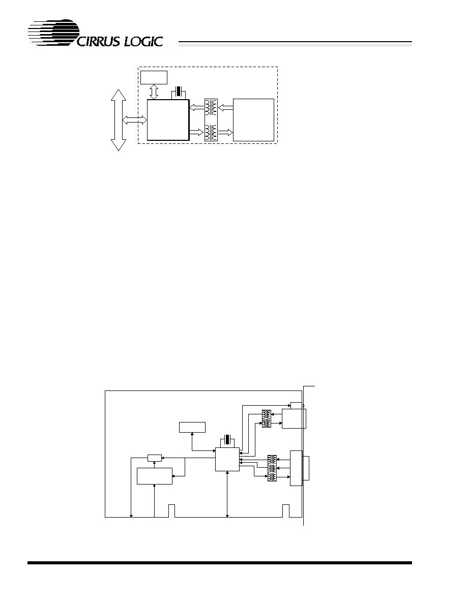
1.2.1 Motherboard LANs
The CS8900A requires the minimum number of
external components needed for a full Ethernet
node. Its small-footprint package and high level of
integration allow System Engineers to design a
complete Ethernet circuit that occupies as little as
1.5 square inches of PCB area (Figure 1). In addi-
tion, the CS8900A's power-saving features and
CMOS design make it a perfect fit for power-sensi-
8
DS271PP4
CS8900A
Crystal LANTM ISA Ethernet Controller
CIRRUS LOGIC PRODUCT DATASHEET
tive portable and desktop PCs. Motherboard design
options include:
�
An EEPROM can be used to store node-specif-
ic information, such as the Ethernet Individual
Address and node configuration.
�
The 20 MHz crystal oscillator may be replaced
by a 20 MHz clock signal.
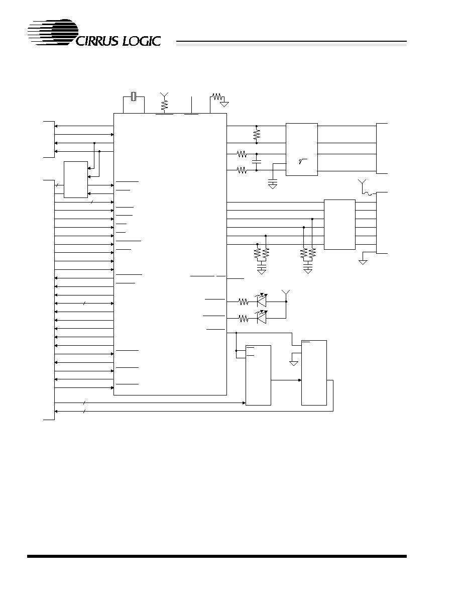
1.2.2 Ethernet Adapter Cards
The CS8900A's highly efficient PacketPage archi-
tecture, with StreamTransferTM
and Auto-Switch
DMA options, make it an excellent choice for high-
performance, low-cost ISA adapter cards
(Figure 2). The CS8900A's wide range of configu-
ration options and performance features allow en-
gineers to design Ethernet solutions that meet their
particular system requirements. Adapter card de-
sign options include:
�
A Boot PROM can be added to support diskless
applications.
�
The 10BASE-T transmitter and receiver im-
pedance can be adjusted to support 100, 120, or
150 Ohm twisted pair cables.
�
An external Latchable-Address-bus decode cir-
cuit can be added to operate the CS8900A in
Upper-Memory space.
�
On-chip LED ports can be used for either op-
tional LEDs, or as programmable outputs.
RJ-45
10BASE-T
CS8900A
I
S
A
EEPROM 20 MHz
XTAL
(2.0 sq. in.)
Figure 1. Complete Ethernet Motherboard Solution
CS8900A
EEPROM
Boot PROM
'245
20 MHz
XTAL
RJ-45
LED
Attachment
Unit
Interface
(AUI)
Figure 2. Full-Featured ISA Adapter Solution

DS271PP4
9
CS8900A
Crystal LANTM ISA Ethernet Controller
CIRRUS LOGIC PRODUCT DATASHEET
1.3 Key Features and Benefits
1.3.1 Very Low Cost
The CS8900A is designed to provide the lowest-
cost Ethernet solution available for embedded ap-
plications, portable motherboards, non-ISA bus
systems and adapter cards. Cost-saving features in-
clude:
�
Integrated RAM eliminates the need for expen-
sive external memory chips.
�
On-chip 10BASE-T filters allow designers to
use simple isolation transformers instead of
more costly filter/transformer packages.
�
The serial EEPROM port, used for configura-
tion and initialization, eliminates the need for
expensive switches and jumpers.
�
The CS8900A is designed to be used on a 2-
layer circuit board instead of a more expensive
multilayer board.
�
The 8900A-based solution offers the smallest
footprint available, saving valuable printed cir-
cuit board area.
�
A set of certified software drivers is available at
no charge, eliminating the need for costly soft-
ware development.
1.3.2 High Performance
The CS8900A is a full 16-bit Ethernet controller
designed to provide optimal system performance
by minimizing time on the ISA bus and CPU over-
head per frame. It offers equal or superior perfor-
mance for less money when compared to other
Ethernet controllers. The CS8900A's PacketPage
architecture allows software to select whichever
access method is best suited to each particular
CPU/ISA-bus configuration. When compared to
older I/O-space designs, PacketPage is faster, sim-
pler and more efficient.
To boost performance further, the CS8900A in-
cludes several key features that increase throughput
and lower CPU overhead, including:
�
StreamTransfer cuts up to 87% of interrupts to
the host CPU during large block transfers.
�
Auto-Switch DMA allows the CS8900A to
maximize throughput while minimizing missed
frames.
�
Early interrupts allow the host to preprocess in-
coming frames.
�
On-chip buffering of full frames cuts the
amount of host bandwidth needed to manage
Ethernet traffic.
1.3.3 Low Power and Low Noise
For low power needs, the CS8900A offers three
power-down options: Hardware Standby, Hard-
ware Suspend, and Software Suspend. In Standby
mode, the chip is powered down with the exception
of the 10BASE-T receiver, which is enabled to lis-
ten for link activity. In either Hardware or Software
Suspend mode, the receiver is disabled and power
consumption drops to the micro-ampere range.
In addition, the CS8900A has been designed for
very low noise emission, thus shortening the time
required for EMI testing and qualification.
1.3.4 Complete Support
The CS8900A comes with a suite of software driv-
ers for immediate use with most industry standard
network operating systems. In addition, complete
evaluation kits and manufacturing packages are
available, significantly reducing the cost and time
required to produce new Ethernet products.
10
DS271PP4
CS8900A
Crystal LANTM ISA Ethernet Controller
CIRRUS LOGIC PRODUCT DATASHEET
EECS
EEDATAOUT
EESK
SA[0:19]
MEMW
MEMR
IOW
IOR
REFRESH
SBHE
SD[0:15]
INTRQ0
INTRQ1
RXD-
RXD+
TXD-
TXD+
DO-
DO+
CI-
CI+
DI-
DI+
LANLED
LINKLED
CSOUT
EEDATAIN
AEN
RESET
INTRQ2
INTRQ3
DMARQ0
DMACK0
DMARQ1
DMACK1
DMARQ2
DMACK2
MEMCS16
IOCHRDY
1:
68 pF
1
3
6
8
24.3
, 1%
24.3
, 1%
92
91
88
87
100
, 1%
RJ45
16
14
11
9
6
3
2
1
1:1
1
4
5
8
84
82
81
79
16
13
12
9
10
10
9
2
5
83
80
2
7
15
3
12
1:1
1:1
0.1
�F
680
680
CE
OE
OE
DIR
20
22
19
1
74LS245
XTAL1 XTAL2
SLEEP
TEST
RES
CS
DO
DI
CLK
1
3
2
4
3
5
4
6
93C46
28
62
61
29
7
IRQ10
IRQ11
IRQ12
IRQ5
DRQ5
DACK5
DRQ6
DACK6
DRQ7
DACK7
16
20
SA[0:19]
LA[20:23]
BALE
4
97
98
93
4.99 k
, 1%
12 V
4, 6
20 MHz
0.1
�F
39.2
, 1%
5 V
4.7 k
CS8900A
CHIPSEL
IOCS16
49
63
75
36
34
64
33
32
30
35
31
15
13
14
16
11
12
99
100
17
39.2
, 1%
39.2
, 1%
39.2
, 1%
EEPROM
Address
Decoder
PAL
27C256
2
ELCS
ISA
BUS
10 BASE T
Isolation
Transformer
1:1
15 pin D
AUI Isolation
Transformer
BSTATUS/HCI
Boot-PROM
PD[0:7]
SA[0:14]
SD[0:7]
15
8
5 V
13
77
76
78
0.1
�F
7
Figure 3. Typical Connection Diagram
DS271PP4
11
CS8900A
Crystal LANTM ISA Ethernet Controller
CIRRUS LOGIC PRODUCT DATASHEET
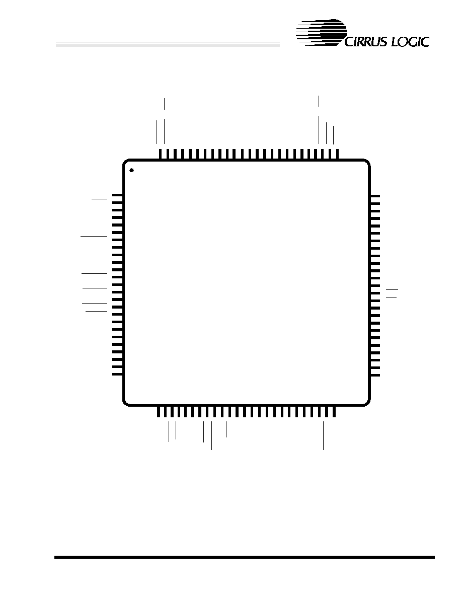
2.0 PIN DESCRIPTION
36
40
41
46
47
48
49
50
26
27
28
29
30
31
33
32
34
35
37
38
39
42
43
44
45
81
82
83
84
85
86
87
88
89
90
91
92
93
94
95
96
97
98
99
10
0
76
77
78
79
80
2
1
3
16
5
4
6
8
7
9
10
11
12
13
14
15
17
18
20
19
21
22
23
24
53
54
55
56
57
58
59
60
61
62
63
64
51
52
65
66
68
67
69
70
71
72
73
74
75
25
EEDataOut
EESK
EECS
EEDataIn
CHIPSEL
DMACK2
DMACK1
DMACK0
DMARQ2
DMARQ1
DMARQ0
SD15
SD14
SD13
SD12
DVDD2
DVSS2
SD11
CSOUT
SD10
SD0
8
SA3
SA4
SA15
SA14
AVS
S
4
BSTAT
U
S
o
r
H
C
1
TXD
+
TXD
-
AVS
S1
AVD
D
1
RX
D -
RX
D
+
AV
S
S
2
AVD
D
2
TEST
SL
EEP
XTAL
1
XT
A
L
2
RE
S
AVS
S
3
SA0
IN
T
R
Q
2
IN
T
R
Q
1
IO
CS
1
6
IN
T
R
Q
0
ME
M
C
S
1
6
SBH
E
SA1
SA2
IN
T
R
Q
3
SA9
SA1
0
SA8
SA1
1
SA5
SA6
SA7
R
E
F
R
ESH
SA19
SA18
SA17
DVDD3
DVSS3
SA16
SD0
AEN
IOW
IOR
IOCHRDY
SD1
SD5
SD4
SD3
SD2
DVSS4
DVDD4
SD6
SD7
LI
N
K
L
E
D
or
H
C
0
RESET
SA13
MEM
W
MEM
R
DVSS1
DVDD1
ELCS
AVSS0
DVSS1A
SD
0
9
SA1
2
DVSS3A
A
V
DD3
LA
N
L
E
D
DO
-
DO
+
DI
-
DI
+
CI
-
CI
+
CS8900A
100-pin
TQFP
(Q)
Top View

12
DS271PP4
CS8900A
Crystal LANTM ISA Ethernet Controller
CIRRUS LOGIC PRODUCT DATASHEET
ISA Bus Interface
SA[0:19] - System Address Bus, Input PINS 37-48, 50-54, 58-60.
Lower 20 bits of the 24-bit System Address Bus used to decode accesses to CS8900A I/O and
Memory space, and attached Boot PROM. SA0-SA15 are used for I/O Read and Write
operations. SA0-SA19 are used in conjunction with external decode logic for Memory Read
and Write operations.
SD[0:15] - System Data Bus, Bi-Directional with 3-State Output PINS 65-68, 71-74, 27-24, 21-18.
Bi-directional 16-bit System Data Bus used to transfer data between the CS8900A and the host.
RESET - Reset, Input PIN 75.
Active-high asynchronous input used to reset the CS8900A. Must be stable for at least 400 ns
before the CS8900A recognizes the signal as a valid reset.
AEN - Address Enable, Input PIN 63.
When TEST is high, this active-high input indicates to the CS8900A that the system DMA
controller has control of the ISA bus. When AEN is high, the CS8900A will not perform slave
I/O space operations. When TEST is low, this pin becomes the shift clock input for the
Boundary Scan Test. AEN should be inactive when performing an IO or memory access and it
should be active during a DMA cycle.
MEMR - Memory Read, Input PIN 29.
Active-low input indicates that the host is executing a Memory Read operation.
MEMW - Memory Write, Input PIN 28.
Active-low input indicates that the host is executing a Memory Write operation.
MEMCS16 - Memory Chip Select 16-bit, Open Drain Output PIN 34.
Open-drain, active-low output generated by the CS8900A when it recognizes an address on the
ISA bus that corresponds to its assigned Memory space (CS8900A must be in Memory Mode
with the MemoryE bit (Register 17, BusCTL, Bit A) set for MEMCS16 to go active). 3-Stated
when not active.
REFRESH - Refresh, Input PIN 49.
Active-low input indicates to the CS8900A that a DRAM refresh cycle is in progress. When
REFRESH is low, MEMR, MEMW, IOR, IOW, DMACK0, DMACK1, and DMACK2 are
ignored.
IOR - I/O Read, Input PIN 61.
When IOR is low and a valid address is detected, the CS8900A outputs the contents of the
selected 16-bit I/O register onto the System Data Bus. IOR is ignored if REFRESH is low.
IOW - I/O Write, Input PIN 62.
When IOW is low and a valid address is detected, the CS8900A writes the data on the System
Data Bus into the selected 16-bit I/O register. IOW is ignored if REFRESH is low.

DS271PP4
13
CS8900A
Crystal LANTM ISA Ethernet Controller
CIRRUS LOGIC PRODUCT DATASHEET
IOCS16 - I/O Chip Select 16-bit, Open Drain Output PIN 33.
Open-drain, active-low output generated by the CS8900A when it recognizes an address on the
ISA bus that corresponds to its assigned I/O space. 3-Stated when not active.
IOCHRDY - I/O Channel Ready, Open Drain Output PIN 64.
When driven low, this open-drain, active-high output extends I/O Read and Memory Read
cycles to the CS8900A. This output is functional when the IOCHRDYE bit in the Bus Control
register (Register 17) is clear. This pin is always 3-Stated when the IOCHRDYE bit is set.
SBHE - System Bus High Enable, Input PIN 36.
Active-low input indicates a data transfer on the high byte of the System Data Bus (SD8-
SD15). After a hardware or a software reset, provide a HIGH to LOW and then LOW to HIGH
transition on SBHE signal before any IO or memory access is done to the CS8900A.
INTRQ[0:3] - Interrupt Request, 3-State PINS 30-32, 35.
Active-high output indicates the presence of an interrupt event. Interrupt Request goes low once
the Interrupt Status Queue (ISQ) is read as all 0's. Only one Interrupt Request output is used
(one is selected during configuration). All non-selected Interrupt Request outputs are placed in
a high-impedance state. (Section 3.2 on page 17 and Section 5.1 on page 78.)
DMARQ[0:2] - DMA Request, 3-State PINS 11, 13, and 15.
Active-high, 3-Stateable output used by the CS8900A to request a DMA transfer. Only one
DMA Request output is used (one is selected during configuration). All non-selected DMA
Request outputs are placed in a high-impedance state.
DMACK[0:2] - DMA Acknowledge, Input PINS 12, 14, and 16.
Active-low input indicates acknowledgment by the host of the corresponding DMA Request
output.
CHIPSEL - Chip Select, Input PIN 7.
Active-low input generated by external Latchable Address bus decode logic when a valid
memory address is present on the ISA bus. If Memory Mode operation is not needed,
CHIPSEL should be tied low. The CHIPSEL is ignored for IO and DMA mode of the
CS8900A.
EEPROM and Boot PROM Interface
EESK - EEPROM Serial Clock, PIN 4.
Serial clock used to clock data into or out of the EEPROM.
EECS - EEPROM Chip Select, PIN 3.
Active-high output used to select the EEPROM.

14
DS271PP4
CS8900A
Crystal LANTM ISA Ethernet Controller
CIRRUS LOGIC PRODUCT DATASHEET
EEDataIn - EEPROM Data In, Input Internal Weak Pullup PIN 6.
Serial input used to receive data from the EEPROM. Connects to the DO pin on the EEPROM.
EEDataIn is also used to sense the presence of the EEPROM.
ELCS - External Logic Chip Select, Internal Weak Pullup PIN 2.
Bi-directional signal used to configure external Latchable Address (LA) decode logic. If
external LA decode logic is not needed, ELCS should be tied low.
EEDataOut - EEPROM Data Out,PIN 5.
Serial output used to send data to the EEPROM. Connects to the DI pin on the EEPROM.
When TEST is low, this pin becomes the output for the Boundary Scan Test.
CSOUT - Chip Select for External Boot PROM, PIN 17.
Active-low output used to select an external Boot PROM when the CS8900A decodes a valid
Boot PROM memory address.
10BASE-T Interface
TXD+/TXD- - 10BASE-T Transmit, Differential Output Pair PINS 87 and 88.
Differential output pair drives 10 Mb/s Manchester-encoded data to the 10BASE-T transmit
pair.
RXD+/RXD- - 10BASE-T Receive, Differential Input Pair PINS 91 and 92.
Differential input pair receives 10 Mb/s Manchester-encoded data from the 10BASE-T receive
pair.
Attachment Unit Interface (AUI)
DO+/DO- - AUI Data Out, Differential Output Pair PINS 83 and 84.
Differential output pair drives 10 Mb/s Manchester-encoded data to the AUI transmit pair.
DI+/DI- - AUI Data In, Differential Input Pair PINS 79 and 80.
Differential input pair receives 10 Mb/s Manchester-encoded data from the AUI receive pair.
CI+/CI- - AUI Collision In, Differential Input Pair PINS 81 and 82.
Differential input pair connects to the AUI collision pair. A collision is indicated by the
presence of a 10 MHz � 15% signal with duty cycle no worse than 60/40.
General Pins
XTAL[1:2] - Crystal, Input/Output PINS 97 and 98.
A 20 MHz crystal should be connected across these pins. If a crystal is not used, a 20 MHz
signal should be connected to XTAL1 and XTAL2 should be left open. (See Section 7.3 on
page 110 and Section 7.7 on page 120.)

DS271PP4
15
CS8900A
Crystal LANTM ISA Ethernet Controller
CIRRUS LOGIC PRODUCT DATASHEET
SLEEP - Hardware Sleep, Input Internal Weak Pullup PIN 77.
Active-low input used to enable the two hardware sleep modes: Hardware Suspend and
Hardware Standby. (See Section 3.7 on page 25.)
LINKLED or HC0 - Link Good LED or Host Controlled Output 0, Open Drain Output PIN 99.
When the HCE0 bit of the Self Control register (Register 15) is clear, this active-low output is
low when the CS8900A detects the presence of valid link pulses. When the HC0E bit is set, the
host may drive this pin low by setting the HCBO in the Self Control register.
BSTATUS or HC1 - Bus Status or Host Controlled Output 1, Open Drain Output PIN 78.
When the HC1E bit of the Self Control register (Register 15) is clear, this active-low output is
low when receive activity causes an ISA bus access. When the HC1E bit is set, the host may
drive this pin low by setting the HCB1 in the Self Control register.
LANLED - LAN Activity LED, Open Drain Output PIN 100.
During normal operation, this active-low output goes low for 6 ms whenever there is a receive
packet, a transmit packet, or a collision. During Hardware Standby mode, this output is driven
low when the receiver detects network activity.
TEST - Test Enable, Input Internal Weak Pullup PIN 76.
Active-low input used to put the CS8900A in Boundary Scan Test mode. For normal operation,
this pin should be high.
RES - Reference Resistor, Input PIN 93.
This input should be connected to a 4.99K
� 1% resistor needed for biasing of internal analog
circuits.
DVDD[1:4] - Digital Power, Power PINS 9, 22, 56, and 69.
Provides 5 V � 5% power to the digital circuits of the CS8900A.
DVSS[1:4} and DVSS1A, DVSS3A - Digital Ground, Ground PINS 8, 10, 23, 55, 57, and 70.
Provides ground reference (0 V) to the digital circuits of the CS8900A.
AVDD[1:3] - Analog Power, Power PINS 90, 85, and 95.
Provides 5 V � 5% power to the analog circuits of the CS8900A.
AVSS[0:4] - Analog Ground, Ground PINS 1, 89, 86, 94, 96.
Provide ground reference (0 V) to the analog circuits of the CS8900A.

16
DS271PP4
CS8900A
Crystal LANTM ISA Ethernet Controller
CIRRUS LOGIC PRODUCT DATASHEET
3.0 FUNCTIONAL DESCRIPTION
3.1 Overview
During normal operation, the CS8900A performs
two basic functions: Ethernet packet transmission
and reception. Before transmission or reception is
possible, the CS8900A must be configured.
3.1.1 Configuration
The CS8900A must be configured for packet trans-
mission and reception at power-up or reset. Various
parameters must be written into its internal Config-
uration and Control registers such as Memory Base
Address; Ethernet Physical Address; what frame
types to receive; and which media interface to use.
Configuration data can either be written to the
CS8900A by the host (across the ISA bus), or load-
ed automatically from an external EEPROM. Oper-
ation can begin after configuration is complete.
Section 3.3 on page 18 and Section 3.4 on page 20
describe the configuration process in detail.
Section 4.4 on page 46 provides a detailed descrip-
tion of the bits in the Configuration and Control
Registers.
3.1.2 Packet Transmission
Packet transmission occurs in two phases. In the
first phase, the host moves the Ethernet frame into
the CS8900A's buffer memory. The first phase be-
gins with the host issuing a Transmit Command.
This informs the CS8900A that a frame is to be
transmitted and tells the chip when to start trans-
mission (i.e. after 5, 381, 1021 or all bytes have
been transferred) and how the frame should be sent
(i.e. with or without CRC, with or without pad bits,
etc.). The Host follows the Transmit Command
with the Transmit Length, indicating how much
buffer space is required. When buffer space is
available, the host writes the Ethernet frame into
the CS8900A's internal memory, either as a Mem-
ory or I/O space operation.
In the second phase of transmission, the CS8900A
converts the frame into an Ethernet packet then
transmits it onto the network. The second phase be-
gins with the CS8900A transmitting the preamble
and Start-of-Frame delimiter as soon as the proper
number of bytes has been transferred into its trans-
mit buffer (5, 381, 1021 bytes or full frame, de-
pending on configuration). The preamble and Start-
of-Frame delimiter are followed by the Destination
Address, Source Address, Length field and LLC
data (all supplied by the host). If the frame is less
than 64 bytes, including CRC, the CS8900A adds
pad bits if configured to do so. Finally, the
CS8900A appends the proper 32-bit CRC value.
The Section 5.7 on page 98 provides a detailed de-
scription of packet transmission.
3.1.3 Packet Reception
Like packet transmission, packet reception occurs
in two phases. In the first phase, the CS8900A re-
ceives an Ethernet packet and stores it in on-chip
memory. The first phase of packet reception begins
with the receive frame passing through the analog
front end and Manchester decoder where Manches-
ter data is converted to NRZ data. Next, the pream-
ble and Start-of-Frame delimiter are stripped off
and the receive frame is sent through the address
filter. If the frame's Destination Address matches
the criteria programmed into the address filter, the
packet is stored in the CS8900A's internal memo-
ry. The CS8900A then checks the CRC, and de-
pending on the configuration, informs the
processor that a frame has been received.
In the second phase, the host transfers the receive
frame across the ISA bus and into host memory.
Receive frames can be transferred as Memory
space operations, I/O space operations, or as DMA
operations using host DMA. Also, the CS8900A
provides the capability to switch between Memory
or I/O operation and DMA operation by using
Auto-Switch DMA and StreamTransfer.
The Section 5.2 on page 78 through Section 5.6 on
page 95 provide a detailed description of packet re-
ception.
DS271PP4
17
CS8900A
Crystal LANTM ISA Ethernet Controller
CIRRUS LOGIC PRODUCT DATASHEET
3.2 ISA Bus Interface
The CS8900A provides a direct interface to ISA
buses running at clock rates from 8 to 11 MHz. Its
on-chip bus drivers are capable of delivering
24 mA of drive current, allowing the CS8900A to
drive the ISA bus directly, without added external
"glue logic".
The CS8900A is optimized for 16-bit data trans-
fers, operating in either Memory space, I/O space,
or as a DMA slave.
Note that ISA-bus operation below 8 MHz should
use the CS8900A's Receive DMA mode to mini-
mize missed frames. See Section 5.4 on page 89 for
a description of Receive DMA operation.
3.2.1 Memory Mode Operation
When configured for Memory Mode operation, the
CS8900A's internal registers and frame buffers are
mapped into a contiguous 4-Kbyte block of host
memory, providing the host with direct access to
the CS8900A's internal registers and frame buff-
ers. The host initiates Read operations by driving
the MEMR pin low and Write operations by driv-
ing the MEMW pin low.
For additional information about Memory Mode,
see Section 4.9 on page 73.
3.2.2 I/O Mode Operation
When configured for I/O Mode operation, the
CS8900A is accessed through eight, 16-bit I/O
ports that are mapped into sixteen contiguous I/O
locations in the host system's I/O space. I/O Mode
is the default configuration for the CS8900A and is
always enabled.
For an I/O Read or Write operation, the AEN pin
must be low, and the 16-bit I/O address on the ISA
System Address bus (SA0 - SA15) must match the
address space of the CS8900A. For a Read, IOR
must be low, and for a Write, IOW must be low.
For additional information about I/O Mode, see
Section 4.10 on page 75.
3.2.3 Interrupt Request Signals
The CS8900A has four interrupt request output
pins that can be connected directly to any four of
the ISA bus Interrupt Request signals. Only one in-
terrupt output is used at a time. It is selected during
initialization by writing the interrupt number (0 to
3) into PacketPage Memory base + 0022h. Unused
interrupt request pins are placed in a high-imped-
ance state. The selected interrupt request pin goes
high when an enabled interrupt is triggered. The
pin goes low after the Interrupt Status Queue (ISQ)
is read as all 0's (see Section 5.1 on page 78 for a
description of the ISQ).
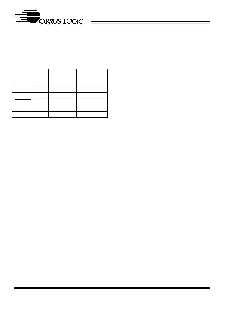
Table 1 presents one possible way of connecting
the interrupt request pins to the ISA bus that utiliz-
es commonly available interrupts and facilitates
board layout.
3.2.4 DMA Signals
The CS8900A interfaces directly to the host DMA
controller to provide DMA transfers of receive
frames from CS8900A memory to host memory.
The CS8900A has three pairs of DMA pins that can
be connected directly to the three 16-bit DMA
channels of the ISA bus. Only one DMA channel is
used at a time. It is selected during initialization by
writing the number of the desired channel (0, 1 or
2) into PacketPage Memory base + 0024h. Unused
DMA pins are placed in a high-impedance state.
The selected DMA request pin goes high when the
CS8900A has received frames to transfer to the
host memory via DMA. If the DMABurst bit (reg-
ister 17, BusCTL, Bit B) is clear, the pin goes low
after the DMA operation is complete. If the
CS8900A Interrupt
Request Pin
ISA Bus
Interrupt
PacketPage
base + 0022h
INTRQ3 (Pin 35)
IRQ5
0003h
INTRQ0 (Pin 32)
IRQ10
0000h
INTRQ1 (Pin 31)
IRQ11
0001h
INTRQ2 (Pin 30)
IRQ12
0002h
Table 1. Interrupt Assignments
18
DS271PP4
CS8900A
Crystal LANTM ISA Ethernet Controller
CIRRUS LOGIC PRODUCT DATASHEET
DMABurst bit is set, the pin goes low 32 �s after
the start of a DMA transfer.
The DMA pin pairs are arranged on the CS8900A
to facilitate board layout. Crystal recommends the
configuration in Table 2 when connecting these
pins to the ISA bus.
For a description of DMA mode, see Section 5.4 on
page 89.
3.3 Reset and Initialization
3.3.1 Reset
Seven different conditions cause the CS8900A to
reset its internal registers and circuits.
3.3.1.1 External Reset, or ISA Reset
There is a chip-wide reset whenever the RESET pin
is high for at least 400 ns. During a chip-wide reset,
all circuitry and registers in the CS8900A are reset.
3.3.1.2 Power-Up Reset
When power is applied, the CS8900A maintains re-
set until the voltage at the supply pins reaches ap-
proximately 2.5 V. The CS8900A comes out of
reset once Vcc is greater than approximately 2.5 V
and the crystal oscillator has stabilized.
3.3.1.3 Power-Down Reset
If the supply voltage drops below approximately
2.5 V, there is a chip-wide reset. The CS8900A
comes out of reset once the power supply returns to
a level greater than approximately 2.5 V and the
crystal oscillator has stabilized.
3.3.1.4 EEPROM Reset
There is a chip-wide reset if an EEPROM check-
sum error is detected (see Section 3.4 on page 20).
3.3.1.5 Software Initiated Reset
There is a chip-wide reset whenever the RESET bit
(Register 15, SelfCTL, Bit 6) is set.
3.3.1.6 Hardware (HW) Standby or Suspend
The CS8900A goes though a chip-wide reset when-
ever it enters or exits either HW Standby mode or
HW Suspend mode (see Section 3.7 on page 25 for
more information about HW Standby and Sus-
pend).
3.3.1.7 Software (SW) Suspend
Whenever the CS8900A enters SW Suspend mode,
all registers and circuits are reset except for the ISA
I/O Base Address register (located at PacketPage
base + 0020h) and the SelfCTL register (Register
15). Upon exit, there is a chip-wide reset (see
Section 3.7 on page 25 for more information about
SW Suspend).
3.3.2 Allowing Time for Reset Operation
After a reset, the CS8900A goes through a self con-
figuration. This includes calibrating on-chip analog
circuitry, and reading EEPROM for validity and
configuration. Time required for the reset calibra-
tion is typically 10 ms. Software drivers should not
access registers internal to the CS8900A during
this time. When calibration is done, bit INITD in
the Self Status Register (register 16) is set indicat-
ing that initialization is complete, and the SIBUSY
bit in the same register is cleared indicating the EE-
PROM is no longer being read or programmed.
3.3.3 Bus Reset Considerations
The CS8900A reads 3000h from IObase+0Ah after
the reset, until the software writes a non-zero value
at IObase+0Ah. The 3000h value can be used as
part of the CS8900A signature when the system
scans for the CS8900A. See Section 4.10 on
page 75.
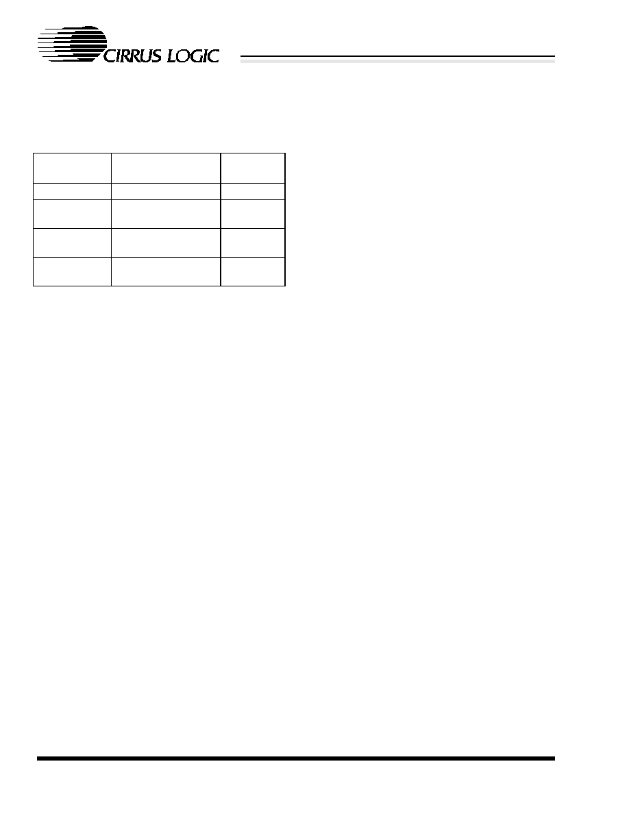
CS8900A DMA
Signal (Pin #)
ISA DMA
Signal
PacketPage
base + 0024h
DMARQ0 (Pin 15)
DRQ5
0000h
DMACK0 (Pin 16)
DACK5
DMARQ1 (Pin 13)
DRQ6
0001h
DMACK1 (Pin 14)
DACK6
DMARQ2 (Pin 11)
DRQ7
0002h
DMACK2 (Pin 12)
DACK7
Table 2. DMA Assignments
DS271PP4
19
CS8900A
Crystal LANTM ISA Ethernet Controller
CIRRUS LOGIC PRODUCT DATASHEET
After a reset, the ISA bus outputs INTRx and
DMARQx are 3-Stated, thus avoiding any interrupt
or DMA channel conflicts on the ISA bus at power-
up time.
3.3.4 Initialization
After each reset (except EEPROM Reset), the
CS8900A checks the sense of the EEDataIn pin to
see if an external EEPROM is present. If EEDI is
high, an EEPROM is present and the CS8900A au-
tomatically loads the configuration data stored in
the EEPROM into its internal registers (see next
section). If EEDI is low, an EEPROM is not
present and the CS8900A comes out of reset with
the default configuration shown in Table 3.
A low-cost serial EEPROM can be used to store
configuration information that is automatically
loaded into the CS8900A after each reset (except
EEPROM reset). The use of an EEPROM is op-
tional.
The CS8900A operates with any of six standard
EEPROM's shown in Table 4.
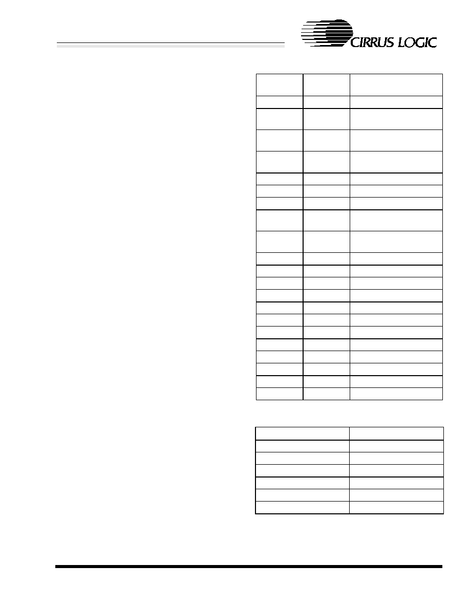
PacketPage
Address
Register
Contents
Register Descriptions
0020h
0300h
I/O Base Address*
0022h
XXXX XXXX
XXXX X100
Interrupt Number
0024h
XXXX XXXX
XXXX XX11
DMA Channel
0026h
0000h
DMA Start of Frame
Offset
0028h
X000h
DMA Frame Count
002Ah
0000h
DMA Byte Count
002Ch
XXX0 0000h Memory Base Address
0030h
XXX0 0000h Boot PROM Base
Address
0034h
XXX0 0000h Boot PROM Address
Mask
0102h
0003h
Register 3 - RxCFG
0104h
0005h
Register 5 - RxCTL
0106h
0007h
Register 7 - TxCFG
0108h
0009h
Register 9 - TxCMD
010Ah
000Bh
Register B - BufCFG
010Ch
Undefined
Reserved
010Eh
Undefined
Reserved
0110h
Undefined
Reserved
0112h
00013h
Register 13 - LineCTL
0114h
0015h
Register 15 - SelfCTL
0116h
0017h
Register 17 - BusCTL
0118h
0019h
Register 19 - TestCTL
* I/O base address is unaffected by Software Suspend mode.
Table 3.
D
efault Configuration
EEPROM Type
Size (16-bit words)
`C46 (non-sequential)
64
`CS46 (sequential)
64
`C56 (non-sequential)
128
`CS56 (sequential)
128
`C66 (non-sequential)
256
`CS66 (sequential)
256
Table 4. Supported EEPROM Types
20
DS271PP4
CS8900A
Crystal LANTM ISA Ethernet Controller
CIRRUS LOGIC PRODUCT DATASHEET
3.4 Configurations with EEPROM
3.4.1 EEPROM Interface
The interface to the EEPROM consists of the four
signals shown in Table 5.
3.4.2 EEPROM Memory Organization
If an EEPROM is used to store initial configuration
information for the CS8900A, the EEPROM is or-
ganized in one or more blocks of 16-bit words. The
first block in EEPROM, referred to as the Configu-
ration Block, is used to configure the CS8900A af-
ter reset. An example of a typical Configuration
Block is shown in Table 6. Additional blocks con-
taining user data may be stored in the EEPROM.
However, the Configuration Block must always
start at address 00h and be stored in contiguous
memory locations.
3.4.3 Reset Configuration Block
The first block in EEPROM, referred to as the Re-
set Configuration Block, is used to automatically
program the CS8900A with an initial configuration
after a reset. Additional user data may also be
stored in the EEPROM if space is available. The
additional data are stored as 16-bit words and can
occupy any EEPROM address space beginning im-
mediately after the end of the Reset Configuration
Block up to address 7Fh, depending on EEPROM
size. This additional data can only be accessed
through software control (refer to Section 3.5 on
page 23 for more information on accessing the EE-
PROM). Address space 80h to AFh is reserved.
3.4.3.1 Reset Configuration Block Structure
The Reset Configuration Block is a block of contig-
uous 16-bit words starting at EEPROM address
00h. It can be divided into three logical sections: a
header, one or more groups of configuration data
words, and a checksum value. All of the words in
the Reset Configuration Block are read sequential-
ly by the CS8900A after each reset, starting with
the header and ending with the checksum. Each
group of configuration data is used to program a
PacketPage register (or set of PacketPage registers
in some cases) with an initial non-default value.
3.4.3.2 Reset Configuration Block Header
The header (first word of the block located at EE-
PROM address 00h) specifies the type of EE-
PROM used, whether or not a Reset Configuration
block is present, and if so, how many bytes of con-
figuration data are stored in the Reset Configura-
tion Block.
3.4.3.3 Determining the EEPROM Type
The LSB of the high byte of the header indicates
the type of EEPROM attached: sequential or non-
sequential. An LSB of 0 (XXXX-XXX0) indicates
a sequential EEPROM. An LSB of 1 (XXXX-
XXX1) indicates a non-sequential EEPROM. The
CS8900A works equally well with either type of
EEPROM. The CS8900A will automatically gen-
erate sequential addresses while reading the Reset
Configuration Block if a non-sequential EEPROM
is used.
3.4.3.4 Checking EEPROM for presence of Reset
Configuration Block
The read-out of either a binary 101X-XXX0 or
101X-XXX1 (X = do not care) from the high byte
of the header indicates the presence of configura-
tion data. Any other readout value terminates ini-
tialization from the EEPROM. If an EEPROM is
attached but not used for configuration, Crystal rec-
ommends that the high byte of the first word be
programmed with 00h in order to ensure that the
CS8900A Pin
(Pin #)
CS8900A Function
EEPROM
Pin
EECS (Pin 3)
EEPROM Chip Select
Chip Select
EESK (PIN 4)
1 MHz EEPROM
Serial Clock output
Clock
EEDO (Pin 5)
EEPROM Data Out
(data to EEPROM)
Data In
EEDI (Pin 6)
EEPROM Data in
(data from EEPROM)
Data Out
Table 5. EEPROM Interface

DS271PP4
21
CS8900A
Crystal LANTM ISA Ethernet Controller
CIRRUS LOGIC PRODUCT DATASHEET
CS8900A will not attempt to read configuration
data from the EEPROM.
3.4.3.5 Determining Number of Bytes in the Reset
Configuration Block
The low byte of the Reset Configuration Block
header is known as the link byte. The value of the
Link Byte represents the number of bytes of config-
uration data in the Reset Configuration Block. The
two bytes used for the header are excluded when
calculating the Link Byte value.
For example, a Reset Configuration Block header
of A104h indicates a non-sequential EEPROM pro-
grammed with a Reset Configuration Block con-
taining 4 bytes of configuration data. This Reset
Configuration Block occupies 6 bytes (3 words) of
EEPROM space (2 bytes for the header and 4 bytes
of configuration data).
3.4.4 Groups of Configuration Data
Configuration data are arranged as groups of
words. Each group contains one or more words of
data that are to be loaded into PacketPage registers.
Word Address
Value
Description
FIRST WORD in DATA BLOCK
00h
A120h
Configuration Block Header.
The high byte, A1h, indicates a `C46 EEPROM is attached. The Link Byte,
20h, indicates the number of bytes to be used in this block of configuration
data.
FIRST GROUP of WORDS
01h
2020h
Group Header for first group of words.
Three words to be loaded, beginning at 0020h in PacketPage memory.
02h
0300h
I/O Base Address
03h
0003h
Interrupt Number
04h
0001h
DMA Channel Number
SECOND GROUP of WORDS
05h
502Ch
Group Header for second group of words.
Six words to be loaded, beginning at 002Ch in PacketPage memory.
06h
E000h
Memory Base Address - low word
07
000Fh
Memory Base Address - high word
08h
0000h
Boot PROM Base Address - low word
09h
000Dh
Boot PROM Base Address - high word
0Ah
C000h
Boot PROM Address Mask - low word
0Bh
000Fh
Boot PROM Address Mask - high word
THIRD GROUP of WORDS
0Ch
2158h
Group Header for third group of words.
Three words to be loaded, beginning at 0158 in PacketPage memory.
0Dh
0010h
Individual Address - Octet 0 and 1
0Eh
0000h
Individual Address - Octet 2 and 3
0Fh
0000h
Individual Address - Octet 4 and 5
CHECKSUM Value
10h
2800h
The high byte, 28h, is the Checksum Value. In this example, the check-
sum includes word addresses 00h through 0Fh. The hexadecimal sum of
the bytes is D8h, resulting in a 2's complement of 28h. The low byte, 00h,
provides a pad to the word boundary.
* FFFFh is a special code indicating that there are no more words in the EEPROM.
Table 6. EEPROM Configuration Block Example

22
DS271PP4
CS8900A
Crystal LANTM ISA Ethernet Controller
CIRRUS LOGIC PRODUCT DATASHEET
The first word of each group is referred to as the
Group Header. The Group Header indicates the
number of words in the group and the address of the
PacketPage register into which the first data word
in the group is to be loaded. Any remaining words
in the group are stored in successive PacketPage
registers.
3.4.4.1 Group Header
Bits F through C of the Group Header specify the
number of words in each group that are to be trans-
ferred to PacketPage registers (see Figure 4). This
value is two less than the total number of words in
the group, including the Group Header. For exam-
ple, if bits F through C contain 0001, there are three
words in the group (a Group Header and two words
of configuration data).
Bits 8 through 0 of the Group Header specify a 9-
bit PacketPage Address. This address defines the
PacketPage register that will be loaded with the
first word of configuration data from the group.
Bits B though 9 of the Group Header are forced to
0, restricting the destination address range to the
first 512 bytes of PacketPage memory. Figure 4
shows the format of the Group header.
3.4.5 Reset Configuration Block Checksum
A checksum is stored in the high byte position of
the word immediately following the last group of
data in the Reset Configuration Block. (The EE-
PROM address of the checksum value can be deter-
mined by dividing the value stored in the Link Byte
by two). The checksum value is the 2's comple-
ment of the 8-bit sum (any carry out of eighth bit is
ignored) of all the bytes in the Reset Configuration
Block, excluding the checksum byte. This sum in-
cludes the Reset Configuration Block header at ad-
dress 00h. Since the checksum is calculated as the
2's complement of the sum of all preceding bytes in
the Reset Configuration Block, a total of 0 should
result when the checksum value is added to the sum
of the previous bytes.
3.4.6 EEPROM Example
Table 6 shows an example of a Reset Configuration
Block stored in a C46 EEPROM. Note that little-
endian word ordering is used, i.e., the least signifi-
cant word of a multiword datum is located at the
lowest address.
3.4.7 EEPROM Read-out
If the EEDI pin is asserted high at the end of reset,
the CS8900A reads the first word of EEPROM data
by:
1) Asserting EECS
2) Clocking out a Read-Register-00h command
on EEDO (EESK provides a 1MHz serial clock
signal)
3) Clocking the data in on EEDI.
If the EEDI pin is low at the end of the reset signal,
the CS8900A does not perform an EEPROM read-
out (uses its default configuration).
3.4.7.1 Determining EEPROM Size
The CS8900A determines the size of the EEPROM
by checking the sense of EEDI on the tenth rising
edge of EESK. If EEDI is low, the EEPROM is a
1
0
3 2
5
4
7 6
First Word of a Group of Words
9 8
B A
D C
F
E
Number of Words
in Group
0
0
9-bit PacketPage Address
0
Figure 4. Group Header

DS271PP4
23
CS8900A
Crystal LANTM ISA Ethernet Controller
CIRRUS LOGIC PRODUCT DATASHEET
'C46 or 'CS46. If EEDI is high, the EEPROM is a
'C56, 'CS56, 'C66, or 'CS66.
3.4.7.2 Loading Configuration Data
The CS8900A reads in the first word from the EE-
PROM to determine if configuration data is con-
tained in the EEPROM. If configuration data is not
stored in the EEPROM, the CS8900A terminates
initialization from EEPROM and operates using its
default configuration (See Table 3). If configura-
tion data is stored in EEPROM, the CS8900A auto-
matically loads all configuration data stored in the
Reset Configuration Block into its internal Pack-
etPage registers.
3.4.8 EEPROM Read-out Completion
Once all the configuration data are transferred to
the appropriate PacketPage registers, the CS8900A
performs a checksum calculation to verify the Re-
set Configuration Blocks data are valid. If the re-
sulting total is 0, the read-out is considered valid.
Otherwise, the CS8900A initiates a partial reset to
restore the default configuration.
If the read-out is valid, the EEPROMOK bit (Reg-
ister 16, SelfST, bit A) is set. EEPROMOK is
cleared if a checksum error is detected. In this case,
the CS8900A performs a partial reset and is re-
stored to its default. Once initialization is complete
(configuration loaded from EEPROM or reset to
default configuration) the INITD bit is set (Register
16, SelfST, bit 7).
3.5 Programming the EEPROM
After initialization, the host can access the EE-
PROM through the CS8900A by writing one of
seven commands to the EEPROM Command regis-
ter (PacketPage base + 0040h). Figure 5 shows the
format of the EEPROM Command register.
3.5.1 EEPROM Commands
The seven commands used to access the EEPROM
are: Read, Write, Erase, Erase/Write Enable,
Erase/Write Disable, Erase-All, and Write-All.
They are described in Table 7.
3.5.2 EEPROM Command Execution
During the execution of a command, the two Op-
code bits, followed by the six bits of address (for a
'C46 or 'CS46) or eight bits of address (for a 'C56,
'CS56, 'C66 or 'CS66), are shifted out of the
CS8900A, into the EEPROM. If the command is a
Write, the data in the EEPROM Data register
(PacketPage base + 0042h) follows. If the com-
mand is a Read, the data in the specified EEPROM
F
X
E
X
D
X
C
X
B
X
ELSEL OP1 OP0
A
9
8
AD5 AD4
5
4
7
6
AD7 AD6
1
0
3
2
AD1 AD0
AD3 AD2
AD5 - AD0 used with
'C46 and 'CS46
AD7 - AD0 used with 'C56,
'CS56, 'C66 and 'CS66
Figure 5. EEPROM Command Register Format
Bit
Name
Description
[F:B]
Reserved
[A]
ELSEL
External Logic Select: When clear, the EECS pin is used to select the EEPROM.
When set, the ELCS pin is used to select the external LA decode circuit.
[9:8]
OP1, OP0
Opcode: Indicates what command is being executed (see next section).
[7:0]
AD7 to AD0
EEPROM Address: Address of EEPROM word being accessed.
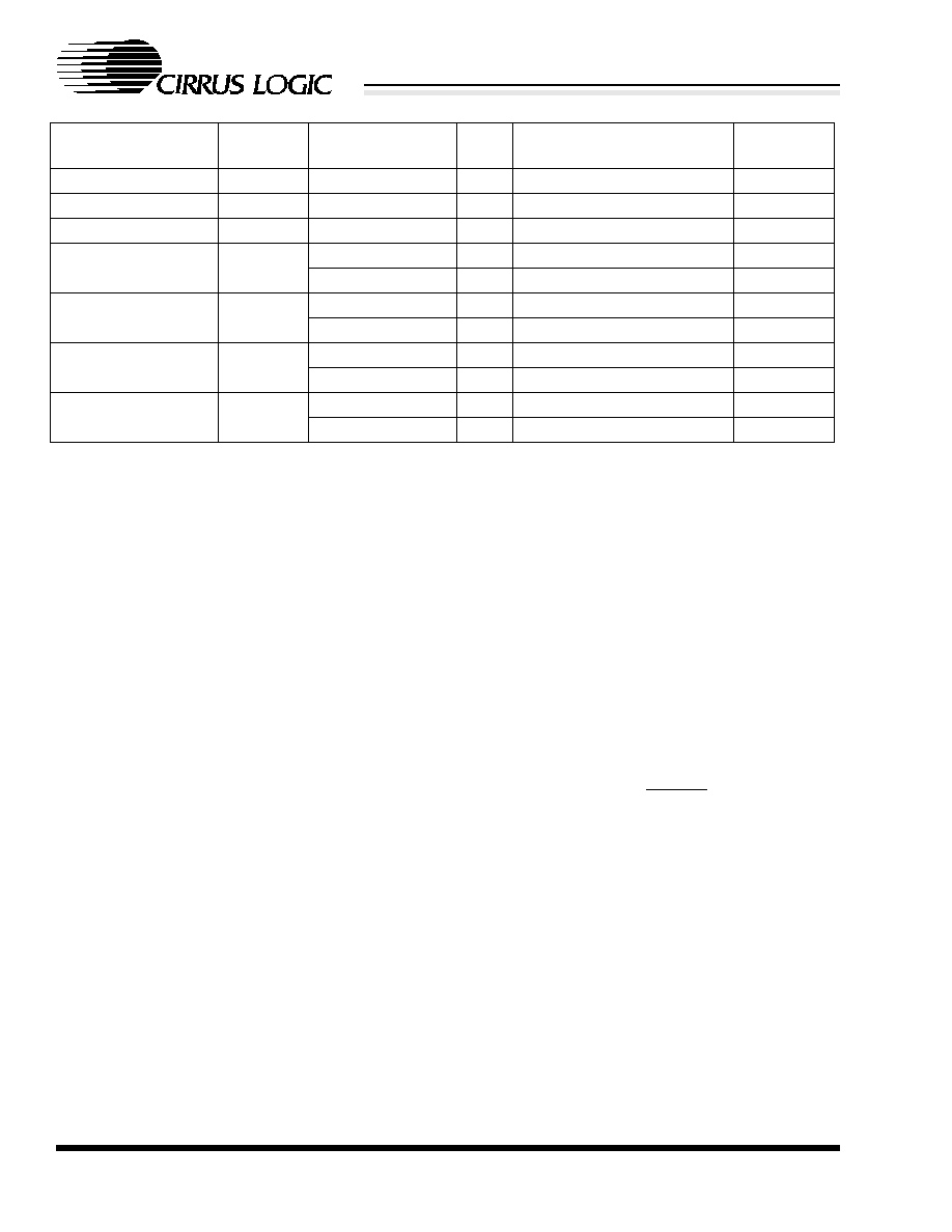
24
DS271PP4
CS8900A
Crystal LANTM ISA Ethernet Controller
CIRRUS LOGIC PRODUCT DATASHEET
location is written into the EEPROM Data register.
If the command is an Erase or Erase-All, no data is
transferred to or from the EEPROM Data register.
Before issuing any command, the host must wait
for the SIBUSY bit (Register 16, SelfST, bit 8) to
clear. After each command has been issued, the
host must wait again for SIBUSY to clear.
3.5.3 Enabling Access to the EEPROM
The Erase/Write Enable command provides protec-
tion from accidental writes to the EEPROM. The
host must write an Erase/Write Enable command
before it attempts to write to or erase any EEPROM
memory location. Once the host has finished alter-
ing the contents of the EEPROM, it must write an
Erase/Write Disable command to prevent unwant-
ed modification of the EEPROM.
3.5.4 Writing and Erasing the EEPROM
To write data to the EEPROM, the host must exe-
cute the following series of commands:
1) Issue an Erase/Write Enable command.
2) Load the data into the EEPROM Data register.
3) Issue a Write command.
4) Issue an Erase/Write Disable command.
During the Erase command, the CS8900A writes
FFh to the specified EEPROM location. During the
Erase-All command, the CS8900A writes FFh to
all locations.
3.6 Boot PROM Operation
The CS8900A supports an optional Boot PROM
used to store code for remote booting from a net-
work server.
3.6.1 Accessing the Boot PROM
To retrieve the data stored in the Boot PROM, the
host issues a Read command to the Boot PROM as
a Memory space access. The CS8900A decodes the
command and drives the CSOUT pin low, causing
the data stored in the Boot PROM to be shifted into
the bus transceiver. The bus transceiver then drives
the data out onto the ISA bus.
3.6.2 Configuring the CS8900A for Boot PROM
Operation
Figure 6 shows how the CS8900A should be con-
nected to the Boot PROM and '245 driver. To con-
figure the CS8900A's internal registers for Boot
PROM operation, the Boot PROM Base Address
must be loaded into the Boot PROM Base Address
register (PacketPage base + 0030h) and the Boot
PROM Address Mask must be loaded into the
Command
Opcode
(bits 9,8)
EEPROM Address
(bits 7 to 0)
Data
EEPROM Type
Execution
Time
Read Register
1,0
word address
yes
all
25 �s
Write Register
0,1
word address
yes
all
10 ms
Erase Register
1.1
word address
no
all
10 ms
Erase/Write Enable
0,0
XX11-XXXX
no
`CS46, `C46
9 �s
11XX-XXXX
no
`CS56, `C56, `CS66, `C66
9 �s
Erase/Write Disable
0,0
0,0
XX00-XXXX
no
`CS46, `C46
9 �s
00XX-XXXX
no
`CS56, `C56, `CS66, `C66
9 �s
Erase-All Registers
0,0
0,0
XX10-XXXX
no
`CS46, `C46
10 ms
10XX-XXXX
no
`CS56, `C56, `CS66, `C66
9 �s
Write-All Register
0,0
0,0
XX01-XXXX
yes
`CS46, `C46
10 ms
01XX-XXXX
yes
`CS56, `C56, `CS66, `C66
10 ms
Table 7. EEPROM Commands

DS271PP4
25
CS8900A
Crystal LANTM ISA Ethernet Controller
CIRRUS LOGIC PRODUCT DATASHEET
BootPROM Address Mask register (PacketPage
base + 0034h). The Boot PROM Base Address pro-
vides the starting location in host memory where
the Boot PROM is mapped. The Boot PROM Ad-
dress Mask indicates the size of the attached Boot
PROM and is limited to 4-Kbyte increments. The
lower 12 bits of the Address Mask are ignored and
should be 000h.
In the EEPROM example shown in Table 6, the
Boot PROM starting address is D0000h and the
Address Mask is FC000h. This configuration de-
scribes a 16-Kbyte (128 Kbit) PROM mapped into
host memory from D0000h to D3FFFh.
3.7 Low-Power Modes
For power-sensitive applications, the CS8900A
supports three low-power modes: Hardware Stand-
by, Hardware Suspend, and Software Suspend. All
three low-power modes are controlled through the
SelfCTL register (Register 15). See also
Section 4.4.4 on page 48.
An internal reset occurs when the CS8900A comes
out of any suspend or standby mode. After a reset
(internal or external), the CS8900A goes through a
self configuration. This includes calibrating on-
chip analog circuitry, and reading EEPROM for va-
lidity and configuration. When the calibration is
done, bit InitD in Register 16 (Self Status register)
is set indicating that initialization is complete, and
the SIBUSY bit in the same register is cleared (in-
dicating that the EEPROM is no longer being read
or programmed. Time required for the reset calibra-
tion is typically 10 ms. Software drivers should not
access registers internal to CS8900A during this
time.
3.7.1 Hardware Standby
Hardware (HW) Standby is designed for use in sys-
tems, such as portable PC's, that may be temporari-
ly disconnected from the 10BASE-T cable. It
allows the system to conserve power while the
LAN is not in use, and then automatically restore
Ethernet operation once the cable is reconnected.
In HW Standby mode, all analog and digital cir-
cuitry in the CS8900A is turned off, except for the
10BASE-T receiver which remains active to listen
for link activity. If link activity is detected, the
LANLED pin is driven low, providing an indica-
tion to the host that the network connection is ac-
tive. The host can then activate the CS8900A by
deasserting the SLEEP pin. During this mode, all
ISA bus accesses are ignored.
To enter HW Standby mode, the SLEEP pin must
be low and the HWSleepE bit (Register 15, Self-
CTL, Bit 9) and the HWStandbyE bit (Register 15,
SelfCTL, Bit A) must be set. When the CS8900A
enters HW Standby, all registers and circuits are re-
set except for the SelfCTL register. Upon exit from
HW Standby, the CS8900A performs a complete
reset, and then goes through normal initialization.
3.7.2 Hardware Suspend
During Hardware Suspend mode, the CS8900A
uses the least amount of current of the three low-
power modes. All internal circuits are turned off
and the CS8900A's core is electronically isolated
from the rest of the system. Accesses from the ISA
bus and Ethernet activity are both ignored.
HW Suspend mode is entered by driving the
SLEEP pin low and setting the HWSleepE bit
(Register 15, SelfCTL, bit 9) while the HWStand-
byE bit (Register 15, SelfCTL, bit A) is clear. To
OE
DIR
B1
.
.
.
B8
A1
.
.
.
A8
74LS245
SD(0:7)
ISA
BUS
SA(0:14)
27C256
CE
OE
20
22
19
CS8900A
CSOUT
(Pin 17)
Figure 6. Boot PROM Connection Diagram
26
DS271PP4
CS8900A
Crystal LANTM ISA Ethernet Controller
CIRRUS LOGIC PRODUCT DATASHEET
exit from this mode, the SLEEP pin must be driven
high. Upon exit, the CS8900A performs a complete
reset, and then goes through a normal initialization
procedure.
3.7.3 Software Suspend
Software (SW) Suspend mode can be used to con-
serve power in applications, like adapter cards, that
do not have power management circuitry available.
During this mode, all internal circuits are shut off
except the I/O Base Address register (PacketPage
base + 0020h) and the SelfCTL register (Register
15).
To enter SW Suspend mode, the host must set the
SWSuspend bit (Register 15, SelfCTL, bit 8). To
exit SW Suspend, the host must write to the
CS8900A's assigned I/O space (the Write is only
used to wake the CS8900A, the Write itself is ig-
nored). Upon exit, the CS8900A performs a com-
plete reset, and then goes through a normal
initialization procedure.
Any hardware reset takes the chip out of any sleep
mode.
Table 8 summarizes the operation of the three low-
power modes.
CS8900A Configuration
CS8900A Operation
SLEEP
(Pin 77)
HWStandbyE
(SelfCTL, Bit A)
HWSleepE
(SelfCTL, Bit 9)
SWSuspend
(SelfCTL, Bit 8) Link Activity
Low
1
1
N/A
Not Present
HW Standby mode: 10BASE-T
receiver listens for link activity
Low
1
1
N/A
Present
HW Standby mode: LANLED low
Low
0
1
N/A
N/A
HW Suspend mode
Low to
High
N/A
1
0
N/A
CS8900A resets and goes through
initialization
High
N/A
N/A
0
N/A
Not in low-power mode
High
N/A
N/A
N/A
SW Suspend mode
Low
N/A
0
1
N/A
SW Suspend mode
Low
N/A
0
0
N/A
Not in low-power mode
Notes: 1. Both HW and HW Suspend take precedence over SW Suspend.
Table 8. Low-Power Mode Operation
DS271PP4
27
CS8900A
Crystal LANTM ISA Ethernet Controller
CIRRUS LOGIC PRODUCT DATASHEET
3.8 LED Outputs
The CS8900A provides three output pins that can
be used to control LEDs or external logic.
3.8.0.1 LANLED
LANLED goes low whenever the CS8900A trans-
mits or receives a frame, or when it detects a colli-
sion. LANLED remains low until there has been no
activity for 6 ms (i.e. each transmission, reception,
or collision produces a pulse lasting a minimum of
6 ms).
3.8.0.2 LINKLED or HC0
LINKLED or HC0 can be controlled by either the
CS8900A or the host. When controlled by the
CS8900A, LINKLED is low whenever the
CS8900A receives valid 10BASE-T link pulses. To
configure this pin for CS8900A control, the HC0E
bit (Register 15, SelfCTL, Bit C) must be clear.
When controlled by the host, LINKLED is low
whenever the HCB0 bit (Register 15, SelfCTL, Bit
E) is set. To configure it for host control, the HC0E
bit must be set. Table 9 summarizes this operation.
3.8.0.3 BSTATUS or HC1
BSTATUS or HC1 can be controlled by either the
CS8900A or the host. When controlled by the
CS8900A, BSTATUS is low whenever the host
reads the RxEvent register (PacketPage base +
0124h), signaling the transfer of a receive frame
across the ISA bus. To configure this pin for
CS8900A control, the HC1E bit (Register 15, Self-
CTL, Bit D) must be clear. When controlled by the
host, BSTATUS is low whenever the HCB1 bit
(Register 15, SelfCTL, Bit F) is set. To configure it
for host control, HC1E must be set. Table 10 sum-
marizes this operation.
3.8.1 LED Connection
Each LED output is capable of sinking 10 mA to
drive an LED directly through a series resistor. The
output voltage of each pin is less than 0.4 V when
the pin is low. Figure 7 shows a typical LED cir-
cuit.
3.9 Media Access Control
3.9.1 Overview
The CS8900A's Ethernet Media Access Control
(MAC) engine is fully compliant with the IEEE
802.3 Ethernet standard (ISO/IEC 8802-3, 1993). It
handles all aspects of Ethernet frame transmission
and reception, including: collision detection, pre-
amble generation and detection, and CRC genera-
HC0E
(Bit C)
HCB0
(Bit E)
Pin Function
0
N/A
Pin configured as LINKLED: Output is
low when valid 10BASE-T link pulses
are detected. Output is high if valid link
pulses are not detected
1
0
Pin configured as HC0:
Output is high
1
1
Pin configured as HC0:
Output is low
Table 9. LINKLED/HC0 Pin Operation
HC1E
(Bit D)
HCB1
(Bit F)
Pin Function
0
N/A
Pin configured as BSTATUS: Output is
low when a receive frame begins trans-
fer across the ISA bus. Output is high
otherwise
1
0
Pin configured as HC1:
Output is high
1
1
Pin configured as HC1:
Output is low
Table 10. BSTATUS/HCI Pin Operation
+5V
LANLED
LINKLED
Figure 7. LED Connection Diagram
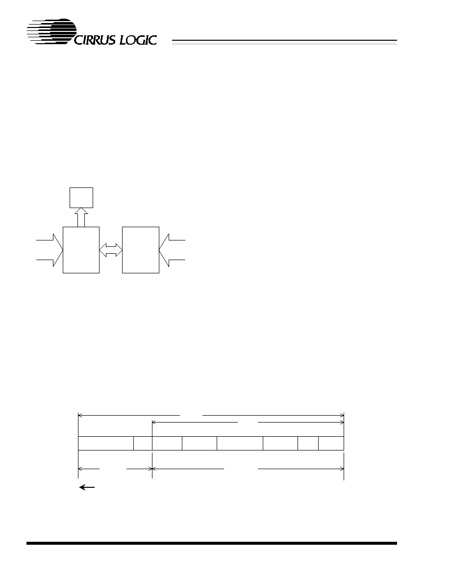
28
DS271PP4
CS8900A
Crystal LANTM ISA Ethernet Controller
CIRRUS LOGIC PRODUCT DATASHEET
tion and test. Programmable MAC features include
automatic retransmission on collision, and padding
of transmitted frames.
Figure 8 shows how the MAC engine interfaces to
other CS8900A functions. On the host side, it inter-
faces to the CS8900A's internal data/address/con-
trol bus. On the network side, it interfaces to the
internal Manchester encoder/decoder (ENDEC).
The primary functions of the MAC are: frame en-
capsulation and decapsulation; error detection and
handling; and, media access management.
3.9.2 Frame Encapsulation and Decapsulation
The CS8900A's MAC engine automatically as-
sembles transmit packets and disassembles receive
packets. It also determines if transmit and receive
frames are of legal minimum size.
3.9.2.1 Transmission
Once the proper number of bytes have been trans-
ferred to the CS8900A's memory (either 5, 381,
1021 bytes, or full frame), and providing that ac-
cess to the network is permitted, the MAC automat-
ically transmits the 7-byte preamble (1010101b...),
followed by the Start-of-Frame Delimiter (SFD,
10101011b), and then the serialized frame data. It
then transmits the Frame Check Sequence (FCS).
The data after the SFD and before the FCS (Desti-
nation Address, Source Address, Length, and data
field) is supplied by the host. FCS generation by the
CS8900A may be disabled by setting the Inhibit-
CRC bit (Register 9, TxCMD, bit C).
Figure 9 shows the Ethernet frame format.
3.9.2.2 Reception
The MAC receives the incoming packet as a serial
stream of NRZ data from the Manchester encod-
er/decoder. It begins by checking for the SFD.
Once the SFD is detected, the MAC assumes all
subsequent bits are frame data. It reads the DA and
compares it to the criteria programmed into the ad-
dress filter (see Section 5.3 on page 86 for a de-
scription of Address Filtering). If the DA passes the
address filter, the frame is loaded into the
CS8900A's memory. If the BufferCRC bit (Regis-
ter 3, RxCFG, bit B) is set, the received FCS is also
loaded into memory. Once the entire packet has
been received, the MAC validates the FCS. If an er-
ror is detected, the CRCerror bit (Register 4, Rx-
Event, Bit C) is set.
3.9.2.3 Enforcing Minimum Frame Size
The MAC provides minimum frame size enforce-
802.3
MAC
Engine
Encoder/
Decoder
&
PLL
LED
Logic
CS8900A
Internal Bus
10BASE-T
& AUI
Figure 8. MAC Interface
1 byte
up to 7 bytes
6 bytes
6 bytes
2 bytes
LLC data
Pad
FCS
4 bytes
preamble
frame length
min 64 bytes
max 1518 bytes
alternating 1s / 0s
SFD
DA
SA
SFD = Start of Frame Delimiter
DA = Destination Address
SA = Source Address
Direction of Transmission
Frame
Packet
LLC = Logical Link Control
FCS = Frame Check Sequence (also
called Cyclic Redundancy Check, or CRC)
Length Field
Figure 9. Ethernet Frame Format

DS271PP4
29
CS8900A
Crystal LANTM ISA Ethernet Controller
CIRRUS LOGIC PRODUCT DATASHEET
ment of both transmit and receive packets. When
the TxPadDis bit (Register 9, TxCMD, Bit D) is
clear, transmit frames will be padded with addition-
al bits to ensure that the receiving station receives a
legal frame (64 bytes, including CRC). When Tx-
PadDis is set, the CS8900A will not add pad bits
and will transmit frames less that 64 bytes. If a
frame is received that is less than 64 bytes (includ-
ing CRC), the Runt bit (Register 4, RxEvent, Bit D)
will be set indicating the arrival of an illegal frame.
3.9.3 Transmit Error Detection and Handling
The MAC engine monitors Ethernet activity and
reports and recovers from a number of error condi-
tions. For transmission, the MAC reports the fol-
lowing errors in the TxEvent register (Register 8)
and BufEvent register (Register C):
3.9.3.1 Loss of Carrier
Whenever the CS8900A is transmitting on the AUI
port, it expects to see its own transmission "looped
back" to its receiver. If it is unable to monitor its
transmission after the end of the preamble, the
MAC reports a loss-of-carrier error by setting the
Loss-of-CRS bit (Register 8, TxEvent, Bit 6). If the
Loss-of-CRSiE bit (Register 7, TxCFG, Bit 6) is
set, the host will be interrupted.
3.9.3.2 SQE Error
After the end of transmission on the AUI port, the
MAC expects to see a collision within 64 bit times.
If no collision is detected, the SQEerror bit (Regis-
ter 8, TxEvent, Bit 7) is set. If the SQEerroriE bit is
set (Register 7, TxCFG, Bit 7), the host is interrupt-
ed. An SQE error may indicate a fault on the AUI
cable or a faulty transceiver (it is assumed that the
attached transceiver supports this function).
3.9.3.3 Out-of-Window (Late) Collision
If a collision is detected after the first 512 bits have
been transmitted, the MAC reports a late collision
by setting the Out-of-window bit (Register 8, Tx-
Event, Bit 9). The MAC then forces a bad CRC and
terminates the transmission. If the Out-of-window-
iE bit (Register 7, TxCFG, Bit 9) is set, the host is
interrupted. A late collision may indicate an illegal
network configuration.
3.9.3.4 Jabber Error
If a transmission continues longer than about
26 ms, the MAC disables the transmitter and sets
the Jabber bit (Register 8, TxEvent, Bit A). The
output of the transmitter returns to idle and remains
there until the host issues a new Transmit Com-
mand. If the JabberiE bit (Register 7, TxCFG, Bit
A) is set, the host is interrupted. A Jabber condition
indicates that there may be something wrong with
the CS8900A transmit function. To prevent possi-
ble network faults, the host should clear the trans-
mit buffer. Possible options include:
Reset the chip with either software or hardware re-
set (see Section 3.3 on page 18).
Issue a Force Transmit Command by setting the
Force bit (Register 9, TxCMD, bit 8).
Issue a Transmit Command with the TxLength
field set to zero.
3.9.3.5 Transmit Collision
The MAC counts the number of times an individual
packet must be retransmitted due to network colli-
sions. The collision count is stored in bits B
through E of the TxEvent register (Register 8). If
the packet collides 16 times, transmission of that
packet is terminated and the 16coll bit (Register 8,
TxEvent, Bit F) is set. If the 16colliE bit (Register
7, TxCFG, Bit F) is set, the host will be interrupted
on the 16th collision. A running count of transmit
collisions is recorded in the TxCOL register.
3.9.3.6 Transmit Underrun
If the CS8900A starts transmission of a packet but
runs out of data before reaching the end of frame,
the TxUnderrun bit (Register C, BufEvent, Bit 9) is
set. The MAC then forces a bad CRC and termi-
nates the transmission. If the TxUnderruniE bit

30
DS271PP4
CS8900A
Crystal LANTM ISA Ethernet Controller
CIRRUS LOGIC PRODUCT DATASHEET
(Register B, BufCFG, Bit 9) is set, the host is inter-
rupted.
3.9.4 Receive Error Detection and Handling
The following receive errors are reported in the Rx-
Event register (Register 4):
3.9.4.1 CRC Error
If a frame is received with a bad CRC, the CRCer-
ror bit (Register 4, RxEvent, Bit C) is set. If the
CRCerrorA bit (Register 5, RxCTL, Bit C) is set,
the frame will be buffered by CS8900A. If the
CRCerroriE bit (Register 3, RxCFG. Bit C) is set,
the host is interrupted.
3.9.4.2 Runt Frame
If a frame is received that is shorter than 64 bytes,
the Runt bit (Register 4, RxEvent, Bit D) is set. If
the RuntA bit (Register 5, RxCTL, Bit D) is set, the
frame will still be buffered by CS8900A. If the
RuntiE bit (Register 3, RxCFG. Bit D) is set, the
host is interrupted.
3.9.4.3 Extra Data
If a frame is received that is longer than 1518 bytes,
the Extradata bit (Register 4, RxEvent, Bit E) is set.
If the ExtradataA bit (Register 5, RxCTL, Bit E) is
set, the first 1518 bytes of the frame will still be
buffered by CS8900A. If the ExtradataiE bit (Reg-
ister 3, RxCFG. Bit E) is set, the host is interrupted.
3.9.4.4 Dribble Bits and Alignment Error
Under normal operating conditions, the MAC may
detect up to 7 additional bits after the last full byte
of a receive packet. These bits, known as dribble
bits, are ignored. If dribble bits are detected, the
Dribblebit bit (Register 4, RxEvent, Bit 7) is set. If
both the Dribblebits bit and CRCerror bit
(Register 4, RxEvent, Bit C) are set at the same
time, an alignment error has occurred.
3.9.5 Media Access Management
The Ethernet network topology is a single shared
medium with several attached stations. The Ether-
net protocol is designed to allow each station equal
access to the network at any given time. Any node
can attempt to gain access to the network by first
completing a deferral process (described below) af-
ter the last network activity, and then transmitting a
packet that will be received by all other stations. If
two nodes transmit simultaneously, a collision oc-
curs and the colliding packets are corrupted. Two
primary tasks of the MAC are to avoid network col-
lisions, and then recover from them when they oc-
cur. In addition, when the CS8900A is using the
AUI, the MAC must support the SQE Test function
described in section 7.2.4.6 of the Ethernet stan-
dard.
3.9.5.1 Collision Avoidance
The MAC continually monitors network traffic by
checking for the presence of carrier activity (carrier
activity is indicated by the assertion of the internal
Carrier Sense signal generated by the ENDEC). If
carrier activity is detected, the network is assumed
busy and the MAC must wait until the current
packet is finished before attempting transmission.
The CS8900A supports two schemes for determin-
ing when to initiate transmission: Two-Part Defer-
ral, and Simple Deferral. Selection of the deferral
scheme is determined by the 2-partDefDis bit
(Register 13, LineCTL, Bit D). If the 2-partDefDis
bit is clear, the MAC uses a two-part deferral pro-
cess defined in section 4.2.3.2.1 of the Ethernet
standard (ISO/IEC 8802-3, 1993). If the 2-partDef-
Dis bit is set, the MAC uses a simplified deferral
scheme. Both schemes are described below:
3.9.5.2 Two-Part Deferral
In the two-part deferral process, the 9.6 �s Inter
Packet Gap (IPG) timer is started whenever the in-
ternal Carrier Sense signal is deasserted. If activity
is detected during the first 6.4 �s of the IPG timer,
the timer is reset and then restarted once the activi-
ty has stopped. If there is no activity during the first
6.4 �s of the IPG timer, the IPG timer is allowed to
time out (even if network activity is detected during

DS271PP4
31
CS8900A
Crystal LANTM ISA Ethernet Controller
CIRRUS LOGIC PRODUCT DATASHEET
the final 3.2 �s). The MAC then begins transmis-
sion if a transmit packet is ready and if it is not in
Backoff (Backoff is described later in this section).
If no transmit packet is pending, the MAC contin-
ues to monitor the network. If activity is detected
before a transmit frame is ready, the MAC defers to
the transmitting station and resumes monitoring the
network.
The two-part deferral scheme was developed to
prevent the possibility of the IPG being shortened
due to a temporary loss of carrier. Figure 10 dia-
grams the two-part deferral process.
3.9.5.3 Simple Deferral
In the simple deferral scheme, the IPG timer is
started whenever Carrier Sense is deasserted. Once
the IPG timer is finished (after 9.6 �s), if a transmit
frame is pending and if the MAC is not in Backoff,
transmission begins the 9.6 �s IPG). If no transmit
packet is pending, the MAC continues to monitor
the network. If activity is detected before a transmit
frame is ready, the MAC defers to the transmitting
station and resumes monitoring the network. Fig-
ure 11 diagrams the simple deferral process.
3.9.5.4 Collision Resolution
If a collision is detected while the CS8900A is
transmitting, the MAC responds in one of three
ways depending on whether it is a normal collision
(within the first 512 bits of transmission) or a late
collision (after the first 512 bits of transmission):
3.9.5.5 Normal Collisions
If a collision is detected before the end of the pre-
amble and SFD, the MAC finishes the preamble
and SFD, transmits the jam sequence (32-bit pat-
tern of all 0's), and then initiates Backoff. If a col-
lision is detected after the transmission of the
preamble and SFD but before 512 bit times, the
MAC immediately terminates transmission, trans-
mits the jam sequence, and then initiates Backoff.
In either case, if the Onecoll bit (Register 9, TxC-
MD, Bit 9) is clear, the MAC will attempt to trans-
mit a packet a total of 16 times (the initial attempt
plus 15 retransmissions) due to normal collisions.
On the 16th collision, it sets the 16coll bit
(Register 8, TxEvent, Bit F) and discards the pack-
et. If the Onecoll bit is set, the MAC discards the
packet without attempting any retransmission.
Transmit
Frame
Start Monitoring
Network Activity
IPG
Timer =
6.4
�s?
Network
Active?
Network
Active?
Start IPG
Timer
Network
Active?
Yes
No
Yes
Yes
Yes
No
No
No
No
Wait
3.2
�s
Yes
Tx
Frame
Ready and Not
in Backoff?
Figure 10. Two-Part Deferral

32
DS271PP4
CS8900A
Crystal LANTM ISA Ethernet Controller
CIRRUS LOGIC PRODUCT DATASHEET
3.9.5.6 Late Collisions
If a collision is detected after the first 512 bits have
been transmitted, the MAC immediately terminates
transmission, transmits the jam sequence, discards
the packet, and sets the Out-of-window bit (Regis-
ter 8, TxEvent, Bit 9). The CS8900A does not ini-
tiate backoff or attempt to retransmit the frame. For
additional information about Late Collisions, see
Out-of-Window Error in this section.
3.9.5.7 Backoff
After the MAC has completed transmitting the jam
sequence, it must wait, or "Back off", before at-
tempting to transmit again. The amount of time it
must wait is determined by one of two Backoff al-
gorithms: the Standard Backoff algorithm
(ISO/IEC 4.2.3.2.5) or the Modified Backoff algo-
rithm. The host selects which algorithm through
the ModBackoffE bit (Register 13, LineCTL,
Bit B).
3.9.5.8 Standard Backoff
The Standard Backoff algorithm, also called the
"Truncated Binary Exponential Backoff", is de-
scribed by the equation:
0
r 2
k
where r (a random integer) is the number of slot
times the MAC must wait (1 slot time = 512 bit
times), and k is the smaller of n or 10, where n is the
number of retransmission attempts.
3.9.5.9 Modified Backoff
The Modified Backoff is described by the equation:
0
r 2
k
where r (a random integer) is the number of slot
times the MAC must wait, and k is 3 for n < 3 and
k is the smaller of n or 10 for n
3, where n is the
number of retransmission attempts.
The advantage of the Modified Backoff algorithm
over the Standard Backoff algorithm is that it re-
duces the possibility of multiple collisions on the
first three retries. The disadvantage is that it ex-
tends the maximum time needed to gain access to
the network for the first three retries.
The host may choose to disable the Backoff algo-
rithm altogether by setting the DisableBackoff bit
(Register 19, TestCTL, Bit B). When disabled, the
CS8900A only waits the 9.6 �s IPG time before
starting transmission.
3.9.5.10 SQE Test
If the CS8900A is transmitting on the AUI, the ex-
ternal transceiver should generate an SQE Test sig-
nal on the CI+/CI- pair following each
transmission. The SQE Test is a 10 MHz signal
lasting 5 to 15 bit times and starting within 0.6 to
Tx
Fra
m
e
Ready and Not
in Backoff?
Transmit
Frame
Start Monitoring
Network Activity
Network
Active?
Network
Active?
Yes
No
Yes
No
No
Yes
Wait
9.6
�s
Figure 11. Simple Deferral

DS271PP4
33
CS8900A
Crystal LANTM ISA Ethernet Controller
CIRRUS LOGIC PRODUCT DATASHEET
1.6 �s after the end of transmission. During this pe-
riod, the CS8900A ignores receive carrier activity
(see SQE Error in this section for more informa-
tion).
3.10 Encoder/Decoder (ENDEC)
The CS8900A's integrated encoder/decoder (EN-
DEC) circuit is compliant with the relevant por-
tions of section 7 of the Ethernet standard (ISO/IEC
8802-3, 1993). Its primary functions include:
Manchester encoding of transmit data; informing
the MAC when valid receive data is present (Carri-
er Detection); and, recovering the clock and NRZ
data from incoming Manchester-encoded data.
Figure 12 provides a block diagram of the ENDEC
and how it interfaces to the MAC, AUI and
10BASE-T transceiver.
3.10.1 Encoder
The encoder converts NRZ data from the MAC and
a 20 MHz Transmit Clock signal into a serial
stream of Manchester data. The Transmit Clock is
produced by an on-chip oscillator circuit that is
driven by either an external 20 MHz quartz crystal
or a TTL-level CMOS clock input. If a CMOS in-
put is used, the clock should be 20 MHz
�0.01%
with a duty cycle between 40% and 60%. The spec-
ifications for the crystal are described in
Section 7.7 on page 120. The encoded signal is
routed to either the 10BASE-T transceiver or AUI,
depending on configuration.
3.10.2 Carrier Detection
The internal Carrier Detection circuit informs the
MAC that valid receive data is present by asserting
the internal Carrier Sense signal as soon it detects a
valid bit pattern (1010b or 0101b for 10BASE-T,
and 1b or 0b for AUI). During normal packet recep-
tion, Carrier Sense remains asserted while the
frame is being received, and is deasserted 1.3 to 2.3
bit times after the last low-to-high transition of the
End-of-Frame (EOF) sequence. Whenever the re-
ceiver is idle (no receive activity), Carrier Sense is
deasserted. The CRS bit (Register 14, LineST,
Bit E) reports the state of the Carrier Sense signal.
3.10.3 Clock and Data Recovery
When the receiver is idle, the phase-lock loop
(PLL) is locked to the internal clock signal. The as-
sertion of the Carrier Sense signal interrupts the
PLL. When it restarts, it locks on the incoming da-
ta. The receive clock is then compared to the in-
coming data at the bit cell center and any phase
difference is corrected. The PLL remains locked as
long as the receiver input signal is valid. Once the
PLL has locked on the incoming data, the ENDEC
converts the Manchester data to NRZ and passes
the decoded data and the recovered clock to the
MAC for further processing.
Encoder
Carrier
Detector
Decoder
& PLL
RX
MUX
TX
MUX
RXSQL
AUISQL
RX
TX
AUIRX
AUITX
AUICol
Clock
Carrier Sense
RX CLK
RX NRZ
TXCLK
TX NRZ
TEN
Port Select
Collision
MAC
ENDEC
10BASE-T
Transceiver
AUI
Figure 12. ENDEC

34
DS271PP4
CS8900A
Crystal LANTM ISA Ethernet Controller
CIRRUS LOGIC PRODUCT DATASHEET
3.10.4 Interface Selection
Physical interface selection is determined by AUI-
only bit (Bit 8) and the AutoAUI/10BT (Bit 9) in
the LineCTL register (Register 13). Table 11 de-
scribes the possible configurations.
3.10.4.1 10BASE-T Only
When configured for 10BASE-T only operation,
the 10BASE-T transceiver and its interface to the
ENDEC are active, and the AUI is powered down.
3.10.4.2 AUI Only
When configured for AUI-only operation, the AUI
and its interface to the ENDEC are active, and the
10BASE-T transceiver is powered down.
3.10.4.3 Auto-Select
In Auto-Select mode, the CS8900A automatically
selects the 10BASE-T interface and powers down
the AUI if valid packets or link pulses are detected
by the 10BASE-T receiver. If valid packets and
link pulses are not detected, the CS8900A selects
the AUI. Whenever the AUI is selected, the
10BASE-T receiver remains active to listen for link
pulses or packets. If 10BASE-T activity is detect-
ed, the CS8900A switches back to 10BASE-T.
3.11 10BASE-T Transceiver
The CS8900A includes an integrated 10BASE-T
transceiver that is compliant with the relevant por-
tions of section 14 of the Ethernet standard
(ISO/IEC 8802-3, 1993). It includes all analog and
digital circuitry needed to interface the CS8900A
directly to a simple isolation transformer (see
Section 7.5 on page 119 for a connection diagram).
Figure 13 provides a block diagram of the
10BASE-T transceiver.
3.11.1 10BASE-T Filters
The CS8900A's 10BASE-T transceiver includes
integrated low-pass transmit and receive filters,
eliminating the need for external filters or a fil-
ter/transformer hybrid. On-chip filters are gm/c im-
plementations of fifth-order Butterworth low-pass
filters. Internal tuning circuits keep the gm/c ratio
tightly controlled, even when large temperature,
supply, and IC process variations occur. The nom-
inal 3 dB cutoff frequency of the filters is 16 MHz,
and the nominal attenuation at 30 MHz (3rd har-
monic) is -27 dB.
AUIonly
(Bit 8)
AutoAUI/10BT
(Bit 9)
Physical
Interface
0
0
10BASE-T Only
1
N/A
AUI Only
0
1
Auto-Select
Table 11. Interface Selection
RXSQL
RX
TX
Link Pulse
Detector
TX Pre-
Distortion
RX Squelch
RX
Comparator
TX Filters
Filter Tuning
RX Filters
TX Drivers
RXD-
RXD+
TXD-
TXD+
ENDEC
LinkOK
(to MAC)
10BASE-T Transceiver
Figure 13. 10BASE-T Transceiver
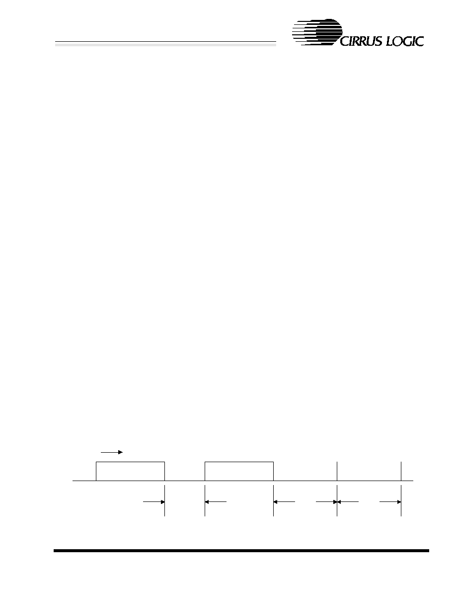
DS271PP4
35
CS8900A
Crystal LANTM ISA Ethernet Controller
CIRRUS LOGIC PRODUCT DATASHEET
3.11.2 Transmitter
When configured for 10BASE-T operation,
Manchester encoded data from the ENDEC is fed
into the transmitter's predistortion circuit where
initial wave shaping and preequalization is per-
formed. The output of the predistortion circuit is
fed into the transmit filter where final wave shaping
occurs and unwanted noise is removed. The signal
then passes to the differential driver where it is am-
plified and driven out of the TXD+/TXD- pins.
In the absence of transmit packets, the transmitter
generates link pulses in accordance with section
14.2.1.1. of the Ethernet standard. Transmitted link
pulses are positive pulses, one bit time wide, typi-
cally generated at a rate of one every 16 ms. The
16 ms timer starts whenever the transmitter com-
pletes an End-of-Frame (EOF) sequence. Thus,
there is a link pulse 16 ms after an EOF unless there
is another transmitted packet. Figure 14 diagrams
the operation of the Link Pulse Generator.
If no link pulses are being received on the receiver,
the 10BASE-T transmitter is internally forced to an
inactive state unless bit DisableLT in register 19
(Test Control register) is set to one.
3.11.3 Receiver
The 10BASE-T receive section consists of the re-
ceive filter, squelch circuit, polarity detection and
correction circuit, and link pulse detector.
3.11.3.1 Squelch Circuit
The 10BASE-T squelch circuit determines when
valid data is present on the RXD+/RXD- pair. In-
coming signals passing through the receive filter
are tested by the squelch circuit. Any signal with
amplitude less than the squelch threshold (either
positive or negative, depending on polarity) is re-
jected.
3.11.3.2 Extended Range
The CS8900A supports an Extended Range feature
that reduces the 10BASE-T receive squelch thresh-
old by approximately 6 dB. This allows the
CS8900A to operate with 10BASE-T cables that
are longer than 100 meters (100 meters is the max-
imum length specified by the Ethernet standard).
The exact additional distance depends on the qual-
ity of the cable and the amount of electromagnetic
noise in the surrounding environment. To activate
this feature, the host must set the LoRxSquelch bit
(Register 13, LineCTL, Bit E).
3.11.4 Link Pulse Detection
To prevent disruption of network operation due to
a faulty link segment, the CS8900A continually
monitors the 10BASE-T receive pair (RXD+/
RXD-) for packets and link pulses. After each
packet or link pulse is received, an internal Link-
Loss timer is started. As long as a packet or link
pulse is received before the Link-Loss timer finish-
es (between 25 and 150 ms), the CS8900A main-
tains normal operation. If no receive activity is
detected, the CS8900A disables packet transmis-
sion to prevent "blind" transmissions onto the net-
work (link pulses are still sent while packet
transmission is disabled). To reactivate transmis-
sion, the receiver must detect a single packet (the
packet itself is ignored), or two link pulses separat-
Time
Link
Pulse
Link
Pulse
16ms
16ms
Less Than
16ms
Packet
Packet
Figure 14. Link Pulse Transmission
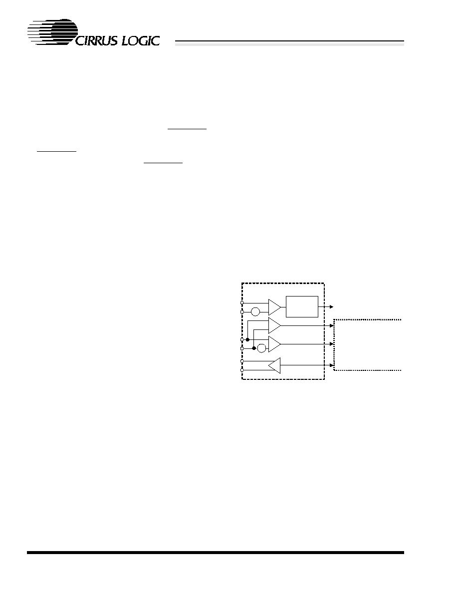
36
DS271PP4
CS8900A
Crystal LANTM ISA Ethernet Controller
CIRRUS LOGIC PRODUCT DATASHEET
ed by more than 2 to 7 ms and no more than 25 to
150 ms (see Section 7.4 on page 112 for 10BASE-
T timing).
The state of the link segment is reported in the
LinkOK bit (Register 14, LineST, Bit 7). If the
HC0E bit (Register 15, SelfCTL, Bit D) is clear, it
is also indicated by the output of the LINKLED
pin. If the link is "good", the LinkOK bit is set and
the LINKLED pin is driven low. If the link is "bad"
the LinkOK bit is clear and the LINKLED pin is
high. To disable this feature, the host must set the
DisableLT bit (Register 19, TestCTL, Bit 7). If
DisableLT is set, the CS8900A will transmit and
receive packets independent of the link segment.
3.11.5 Receive Polarity Detection and Correction
The CS8900A automatically checks the polarity of
the receive half of the twisted pair cable. If the po-
larity is correct, the PolarityOK bit (Register 14,
LineST, bit C) is set. If the polarity is reversed, the
PolarityOK bit is clear. If the PolarityDis bit (Reg-
ister 13, LineCTL, Bit C) is clear, the CS8900A au-
tomatically corrects a reversal. If the PolarityDis
bit is set, the CS8900A does not correct a reversal.
The PolarityOK bit and the PolarityDis bit are in-
dependent.
To detect a reversed pair, the receiver examines re-
ceived link pulses and the End-of-Frame (EOF) se-
quence of incoming packets. If it detects at least
one reversed link pulse and at least four frames in a
row with negative polarity after the EOF, the re-
ceive pair is considered reversed. Any data re-
ceived before the correction of the reversal is
ignored.
3.11.6 Collision Detection
If half-duplex operation is selected (Register 19,
Bit E, FDX), the CS8900A detects a 10BASE-T
collision whenever the receiver and transmitter are
active simultaneously. When a collision is present,
the Collision Detection circuit informs the MAC by
asserting the internal Collision signal (see
Section 3.9 on page 27 for collision handling).
3.12 Attachment Unit Interface (AUI)
The CS8900A Attachment Unit Interface (AUI)
provides a direct interface to external 10BASE2,
10BASE5, and 10BASE-FL Ethernet transceivers.
It is fully compliant with Section 7 of the Ethernet
standard (ISO/IEC 8802-3), and as such, is capable
of driving a full 50-meter AUI cable.
The AUI consists of three pairs of signals: Data Out
(DO+/DO-), Data In (DI+/DI-), and Collision In
(CI+/CI-). To select the AUI, the host should set
the AUI bit (Register 13, LineCTL, Bit 8). The AUI
can also be selected automatically as described in
the previous section (Section 3.10.4 on page 34).
Figure 15 provides a block diagram of the AUI.
(For a connection diagram, see Section 7.6 on
page 120).
3.12.1 AUI Transmitter
The AUI transmitter is a differential driver de-
signed to drive a 78
cable. It accepts data from
the ENDEC and transmits it directly on the
DO+/DO- pins. After transmission has started, the
CS8900A expects to see the packet "looped-back"
(or echoed) to the receiver, causing the Carrier
Sense signal to be asserted. This Carrier Sense
presence indicates that the transmit signal is getting
through to the transceiver. If the Carrier Sense sig-
nal remains deasserted throughout the transmis-
DI+
DI-
DO+
DO-
ENDEC
CL+
CL-
Collision
Detect
AUICol (to MAC)
AUIRX
AUISQL
AUITX
AUI
- +
- +
Figure 15. AUI

DS271PP4
37
CS8900A
Crystal LANTM ISA Ethernet Controller
CIRRUS LOGIC PRODUCT DATASHEET
sion, or if the Carrier Sense signal is deasserted
before the end of the transmission, there is a Loss-
of-Carrier error and the Loss-of-CRS bit (Register
8, TxEvent, Bit 6) is set.
3.12.2 AUI Receiver
The AUI receiver is a differential pair circuit that
connects directly to the DI+/DI- pins. It is designed
to distinguish between transient noise pulses and
incoming Ethernet packets. Incoming packets with
proper amplitude and pulse width are passed on to
the ENDEC section, while unwanted noise is re-
jected.
3.12.3 Collision Detection
The AUI collision circuit is a differential pair re-
ceiver that detects the presence of collision signals
on the CI+/CI- pins. The collision signal is generat-
ed by an external Ethernet transceiver whenever a
collision is detected on the Ethernet segment. (Sec-
tion 7.3.1.2 of ISO/IEC 8802-3, 1993, defines the
collision signal as a 10 MHz � 15% signal with a
duty cycle no worse than 60/40). When a collision
is present, the AUI Collision circuit informs the
MAC by asserting the internal Collision signal.
3.13 External Clock Oscillator
A 20-MHz quartz crystal or CMOS clock input is
required by the CS8900A. If a CMOS clock input
is used, it should be connected the to XTAL1 pin,
with the XTAL2 pin left open. The clock signal
should be 20 MHz
�0.01% with a duty cycle be-
tween 40% and 60%. The specifications for the
crystal are described in Section 7.7 on page 120.

38
DS271PP4
CS8900A
Crystal LANTM ISA Ethernet Controller
CIRRUS LOGIC PRODUCT DATASHEET
4.0 PACKETPAGE ARCHITECTURE
4.1 PacketPage Overview
The CS8900A architecture is based on a unique,
highly-efficient method of accessing internal regis-
ters and buffer memory known as PacketPage.
PacketPage provides a unified way of controlling
the CS8900A in Memory or I/O space that mini-
mizes CPU overhead and simplifies software. It
provides a flexible set of performance features and
configuration options, allowing designers to devel-
op Ethernet circuits that meet their particular sys-
tem requirements.
4.1.1 Integrated Memory
Central to the CS8900A architecture is a 4-Kbyte
page of integrated RAM known as PacketPage
memory. PacketPage memory is used for tempo-
rary storage of transmit and receive frames, and for
internal registers. Access to this memory is done
directly, through Memory space operations
(Section 4.9 on page 73), or indirectly, through I/O
space operations (Section 4.10 on page 75). In
most cases, Memory Mode will provide the best
overall performance, because ISA Memory opera-
tions require fewer cycles than I/O operations. I/O
Mode is the CS8900A's default configuration and
is used when memory space is not available or
when special operations are required (e.g. waking
the CS8900A from the Software Suspend State re-
quires the host to write to the CS8900A's assigned
I/O space).
The user-accessible portion of PacketPage memory
is organized into the following six sections:
4.1.2 Bus Interface Registers
The Bus Interface registers are used to configure
the CS8900A's ISA-bus interface and to map the
CS8900A into the host system's I/O and Memory
space. Most of these registers are written only dur-
ing initialization, remaining unchanged while the
CS8900A is in normal operating mode. The excep-
tions to this are the DMA registers which are mod-
ified continually whenever the CS8900A is using
DMA. These registers are described in more detail
in Section 4.3 on page 41.
4.1.3 Status and Control Registers
The Status and Control registers are the primary
means of controlling and getting status of the
CS8900A. They are described in more detail in
Section 4.4 on page 46.
4.1.4 Initiate Transmit Registers
The TxCMD/TxLength registers are used to initiate
Ethernet frame transmission. These registers are
described in more detail in Section 4.5 on page 70.
(See Section 5.7 on page 98 for a description of
frame transmission.)
4.1.5 Address Filter Registers
The Filter registers store the Individual Address fil-
ter and Logical Address filter used by the Destina-
tion Address (DA) filter. These registers are
described in more detail in Section 4.6 on page 71.
For a description of the DA filter, see Section 5.3
on page 86.
4.1.6 Receive and Transmit Frame Locations
The Receive and Transmit Frame PacketPage loca-
tions are used to transfer Ethernet frames to and
from the host. The host simply writes to and reads
from these locations and internal buffer memory is
dynamically allocated between transmit and re-
ceive as needed. This provides more efficient use
of buffer memory and better overall network per-
formance. As a result of this dynamic allocation,
only one receive frame (starting at PacketPage base
+ 0400h) and one transmit frame (starting at Pack-
PacketPage
Address
Contents
0000h - 0045h
Bus Interface Registers
0100h - 013Fh
Status and Control Registers
0140h - 014Fh
Initiate Transmit Registers
0150h - 015Dh
Address Filter Registers
0400h
Receive Frame Location
0A00h
Transmit Frame Location

DS271PP4
39
CS8900A
Crystal LANTM ISA Ethernet Controller
CIRRUS LOGIC PRODUCT DATASHEET
etPage base + 0A00h) are directly accessible. See
Section 4.7 on page 72.
4.2 PacketPage Memory Map
Table 12 shows the CS8900A PacketPage memory
address map: s
PacketPage
Address
# of
Bytes
Type
Description
Cross Reference
Bus Interface Registers
0000h
4
Read-only Product Identification Code
Section 4.3 on page 41
0004h
28
-
Reserved
Note 2
0020h
2
Read/Write I/O Base Address
Section 4.3 on page 41,
Section 4.7 on page 72
0022h
2
Read/Write Interrupt Number (0,1,2,or 3)
Section 3.2 on page 17,
Section 4.3 on page 41
0024h
2
Read/Write DMA Channel Number (0, 1, or 2)
Section 3.2 on page 17,
Section 4.3 on page 41
0026h
2
Read-only DMA Start of Frame
Section 4.3 on page 41,
Section 5.4 on page 89
0028h
2
Read-only DMA Frame Count (12 Bits)
Sections Section 4.3 on page 41,
"Receive DMA"
002Ah
2
Read-only RxDMA Byte Count
Section 4.3 on page 41,
Section 5.4 on page 89
002Ch
4
Read/Write Memory Base Address Register
(20 Bit)
Section 4.3 on page 41,
Section 4.9 on page 73
0030h
4
Read/Write Boot PROM Base Address
Section 3.6 on page 24,
Section 4.3 on page 41
0034h
4
Read/Write Boot PROM Address Mask
Section 3.6 on page 24,
Section 4.3 on page 41
0038h
8
-
Reserved
Note 2
0040h
2
Read/Write EEPROM Command
Section 3.5 on page 23,
Section 4.3 on page 41
0042h
2
Read/Write EEPROM Data
Section 3.5 on page 23,
Section 4.3 on page 41
0044h
12
-
Reserved
Note 2
0050h
2
Read only Received Frame Byte Counter
Section 4.3 on page 41,
Section 5.2.9 on page 86
0052h
174
-
Reserved
Note 2
Status and Control Registers
0100h
32
Read/Write Configuration & Control Registers
(2 bytes per regiseter)
Section 4.4 on page 46
0120h
32
Read-only Status & Event Registers
(2 bytes per register)
Section 4.4 on page 46
0140h
4
-
Reserved
Note 2
Initiate Transmit Registers
Notes: 1. All registers are accessed as words only.
2. Read operation from the reserved location provides undefined data. Writing to a reserved location or
undefined bits may result in unpredictable operation of the CS8900A.
Table 12. PacketPage Memory Address Map
40
DS271PP4
CS8900A
Crystal LANTM ISA Ethernet Controller
CIRRUS LOGIC PRODUCT DATASHEET
0144h
2
Write-only TxCMD (transmit command)
Section 4.5 on page 70,
Section 5.7 on page 98
0146h
2
Write-only TxLength (transmit length)
Section 4.5 on page 70,
Section 5.7 on page 98
0148h
8
-
Reserved
Note 2
Address Filter Registers
0150h
8
Read/Write Logical Address Filter (hash table)
Section 4.6 on page 71,
Section 5.3 on page 86
0158h
6
Read/Write Individual Address
Section 4.6 on page 71,
Section 5.3 on page 86
015Eh
674
-
Reserved
Note 2
Frame Location
0400h
2
Read-only RXStatus (receive status)
Section 4.7 on page 72,
Section 5.2 on page 78
0402h
2
Read-only RxLength (receive length, in bytes)
Section 4.7 on page 72,
Section 5.2 on page 78
0404h
-
Read-only Receive Frame Location
Section 4.7 on page 72,
Section 5.2 on page 78
0A00
-
Write-only Transmit Frame Location
Section 4.7 on page 72,
Section 5.7 on page 98
PacketPage
Address
# of
Bytes
Type
Description
Cross Reference
Notes: 1. All registers are accessed as words only.
2. Read operation from the reserved location provides undefined data. Writing to a reserved location or
undefined bits may result in unpredictable operation of the CS8900A.
Table 12. PacketPage Memory Address Map
(continued)

DS271PP4
41
CS8900A
Crystal LANTM ISA Ethernet Controller
CIRRUS LOGIC PRODUCT DATASHEET
4.3 Bus Interface Registers
4.3.1 Product Identification Code
(Read only, Address: PacketPage base + 0000h)
The Product Identification Code Register is located in the first four bytes of the PacketPage (0000h to 0003h). The
register contains a unique 32-bit product ID code that identifies the chip as a CS8900A. The host can use this num-
ber to determine which software driver to load and to check which features are available.
Reset value is: 0000 1110 0110 0011 0000 0000 000X XXXX
The X XXXX codes for the CS8900A are:
Rev B: 0 0111
Rev C: 0 1000
Rev D: 0 1001
4.3.2 I/O Base Address
(Read/Write, Address: PacketPage base + 0020h)
The I/O Base Address Register describes the base address for the sixteen contiguous locations in the host system's
I/O space, which are used to access the PacketPage registers. See Section 4.10 on page 75. The default location
is 0300h.
After reset, if no EEPROM is found by the CS8900A, then the register has the following initial state. If an EEPROM
is found, then the register's initial value may be set by the EEPROM. See Section 3.3 on page 18.
Reset value is: 0000 0011 0000 0000
Address 0000h
Address 0001h
Address 0002h
Address 00003h
First byte of EISA registration
number for
Crystal Semiconductor
Second byte of EISA
registration number for Crys-
tal Semiconductor
First 8 bits of
Product ID number
Last 3 bits of the Product ID
number (5 "X" bits are the revi-
sion number)
Address 0021h
Address 0020h
Most significant byte of I/O Base Address
Least significant byte of I/O Base Address
42
DS271PP4
CS8900A
Crystal LANTM ISA Ethernet Controller
CIRRUS LOGIC PRODUCT DATASHEET
4.3.3 Interrupt Number
(Read/Write, Address: PacketPage base + 0022h)
The Interrupt Number Register defines the interrupt pin selected by the CS8900A. In a typical application the follow-
ing bus signals are tied to the following pins:
See Section 3.2 on page 17.
After reset, if no EEPROM is found by the CS8900A, then the register has the following initial state, which corre-
sponds to placing all the INTRQ pins in a high-impedance state. If an EEPROM is found, then the register's initial
value may be set by the EEPROM. See Section 3.3 on page 18.
Reset value is: XXXX XXXX XXXX X100
4.3.4 DMA Channel Number
(Read/Write, Address: PacketPage base + 0024h)
The DMA Channel register defines the DMA pins selected by the CS8900A. In the typical application, the following
bus signals are tied to the following pins:
See Section 3.2 on page 17 and Section 5.4 on page 89.
After reset, if no EEPROM is found by the CS8900A, then the register has the following initial state which corre-
sponds to setting all DMRQ pins to high-impedance. If a EEPROM is found, then the register's initial value may be
set by the EEPROM. See Section 3.3 on page 18.
Reset value is: XXXX XXXX XXXX XX11
Address 0023h
Address 0022h
00h
Interrupt number assignment:
0000 0000b= pin INTRQ0
0000 0001b= pin INTRQ1
0000 0010b= pin INTRQ2
0000 0011b= pin INTRQ3
0000 01XXb= All INTRQ pins high-impedance
Bus signal
Typical pin connection
IRQ5
INTRQ3
IRQ10
INTRQ0
IRQ11
INTRQ1
IRQ12
INTRQ2
Address 0025h
Address 0024h
00h
DMA channel assignment:
0000 0000b= pin DMRQ0 and DMACK0
0000 0001b= pin DMRQ1 and DMACK1
0000 0010b= pin DMRQ2 and DMACK2
0000 0011b= All DMRQ pins high-impedance
Bus signal
Typical pin connection
DRQ5
DACK5
DMRQ0
DMACK0
DRQ6
DACK6
DMRQ1
DMACK1
DRQ7
DACK7
DMRQ2
DMACK2
DS271PP4
43
CS8900A
Crystal LANTM ISA Ethernet Controller
CIRRUS LOGIC PRODUCT DATASHEET
4.3.5 DMA Start of Frame
(Read only, Address: PacketPage base + 0026h)
The DMA Start of Frame Register contains a 16-bit value which defines the offset from the DMA base address to
the start of the most recently transferred received frame. See Section 5.4 on page 89.
Reset value is: 0000 0000 0000 0000
4.3.6 DMA Frame Count
(Read only, Address: PacketPage base + 0028h)
The lower 12 bits of the DMA Frame Count register define the number of valid frames transferred via DMA since the
last readout of this register. The upper 4 bits are reserved. See Section 5.4 on page 89.
Reset value is: XXXX 0000 0000 0000
4.3.7 RxDMA Byte Count
(Read only, Address: PacketPage base + 002Ah)
The RxDMA Byte Count register describes the valid number of bytes DMAed since the last readout. See Section 5.4
on page 89.
Reset value is: 0000 0000 0000 0000
4.3.8 Memory Base Address
(Read/Write, Address: PacketPage base + 002Ch)
Memory Base Address: The lower three bytes (002Ch, 002Dh, and 002Eh) are used for the 20-bit memory base
address. The upper three nibbles are reserved.
After reset, if no EEPROM is found by the CS8900A, then the register has the following initial state. If an EEPROM
is found, then the register's initial value may be set by the EEPROM. See Section 3.3 on page 18.
Reset value is: XXXX XXXX XXXX 0000 0000 0000 0000 0000
Address 0027h
Address 0026h
Most significant byte of offset value
Least significant byte of offset value
Address 0029h
Address 0028h
Most significant byte of frame count
(most-significant nibble always 0h)
Least significant byte of frame count
Address 002Bh
Address 002Ah
Most significant byte of byte count
Least significant byte of byte count
Address 002Fh
Address 002Eh
Address 002Dh
Address 002Ch
Reserved
The most significant nibble of
memory base address. The
high-order nibble is reserved.
Contains portion of memory
base address.
The least significant byte of
the memory base address.

44
DS271PP4
CS8900A
Crystal LANTM ISA Ethernet Controller
CIRRUS LOGIC PRODUCT DATASHEET
4.3.9 Boot PROM Base Address
(Read/Write, Address: PacketPage base + 0030h)
The lower three bytes (0030h, 0031h, and 0032h) of the Boot PROM Base Address register are used for the 20-bit
Boot PROM base address. The upper three nibbles are reserved. See Section 3.6 on page 24.
After reset, if no EEPROM is found by the CS8900A, then the register has the following initial state. If an EEPROM
is found, then the register's initial value may be set by the EEPROM. See Section 3.3 on page 18.
Reset value is: XXXX XXXX XXXX 0000 0000 0000 0000 0000
4.3.10 Boot PROM Address Mask
(Read/Write, Address: PacketPage base + 0034h)
The Boot PROM address mask register indicates the size of the attached Boot PROM and is limited to 4K bit incre-
ments. The lower 12 bits of the Address Mask are ignored, and should be 000h. The next lowest-order bits describe
the size of the PROM. The upper three nibbles are reserved.
For example:
See Section 3.6 on page 24.
After reset, if no EEPROM is found by the CS8900A, then the register has the following initial state. If an EEPROM
is found, then the register's initial value may be set by the EEPROM. See Section 3.3 on page 18.
Reset value is: XXXX XXXX XXXX 0000 0000 0000 0000 0000
Address 0033h
Address 0032h
Address 0031h
Address 0030h
Reserved
The most significant nibble of
Boot PROM base address.
The high-order nibble is
reserved.
Contains portion of Boot PROM
base address.
The least significant byte of
the Boot PROM base
address.
Address 0037h
Address 0036h
Address 0035h
Address 0034h
Reserved
The most significant nibble of
Boot PROM mask address.
The high-order nibble is
reserved.
Contains portion of Boot PROM
mask address. The lower-order
nibble must be written as 0h.
The least significant byte of
the Boot PROM mask
address. Must be written as
00h.
Size of Boot PROM
Register value
4k bits
XXXX XXXX XXXX 1111 1111 0000 0000 0000
8k bits
XXXX XXXX XXXX 1111 1110 0000 0000 0000
16k bits
XXXX XXXX XXXX 1111 1100 0000 0000 0000

DS271PP4
45
CS8900A
Crystal LANTM ISA Ethernet Controller
CIRRUS LOGIC PRODUCT DATASHEET
4.3.11 EEPROM Command
(Read/Write, Address: PacketPage base + 0040h)
This register is used to control the reading, writing and erasing of the EEPROM. See Section 3.5.
ADD7-ADD0
Address of the EEPROM word being accessed.
OB1,OB0
Indicates the Opcode of the command being executed. See Table 7.
ELSEL
External logic select: When clear, the EECS pin is used to select the EEPROM. When set, the
ELCS pin is used to select the external LA decode circuit.
Reserved
Reserved and must be written as 0.
Reset value is: XXXX XXXX XXXX XXXX
4.3.12 EEPROM Data
(Read/Write, Address: PacketPage base + 0042h)
This register contains the word being written to, or read from, the EEPROM. See Section 3.5 on page 23.
Reset value is: XXXX XXXX XXXX XXXX
4.3.13 Receive Frame Byte Counter
(Read only, Address: PacketPage base + 0050h)
This register contains the count of the total number bytes received in the current received frame. This count contin-
uously increments as more bytes in this frame are received. See Section 5.2.9 on page 86.
Reset value is: XXXX XXXX XXXX XXXX
7
6
5
4
3
2
1
0
ADD7 to ADD0
F
E
D
C
B
A
9
8
Reserved
ELSEL
OB1 OB0
Address 0043h
Address 0042h
Most significant byte of the EEPROM data.
Least significant byte of the EEPROM data.
Address 0051h
Address 0050h
Most significant byte of the byte count.
Least significant byte of the byte count.

46
DS271PP4
CS8900A
Crystal LANTM ISA Ethernet Controller
CIRRUS LOGIC PRODUCT DATASHEET
4.4 Status and Control Registers
The Status and Control registers are the primary
registers used to control and check the status of the
CS8900A. They are organized into two groups:
Configuration/Control Registers and Status/Event
Registers. All Status and Control Registers are 16-
bit words as shown in Figure 16. Bit 0 indicates
whether it is a Configuration/Control Register
(Bit 0 = 1) or a Status/Event Register (Bit 0 = 0).
Bits 0 through 5 provide an internal address code
that describes the exact function of the register.
Bits 6 through F are the actual Configuration/Con-
trol and Status/Event bits.
4.4.1 Configuration and Control Registers
Configuration and Control registers are used to set-
up the following:
�
how frames will be transmitted and received;
�
which frames will be transmitted and received;
�
which events will cause interrupts to the host
processor; and,
�
how the Ethernet physical interface will be
configured.
These registers are read/write and are designated
by odd numbers (e.g. Register 1, Register 3, etc.).
The Transmit Command Register (TxCMD) is a
special type of register. It appears in two separate
locations in the PacketPage memory map. The first
location, PacketPage base + 0108h, is within the
block of Configuration/Control Registers and is
read-only. The second location, PacketPage base +
0144h, is where the actual transmit commands are
issued and is write-only. See Section 4.4.4 on
page 48 (Register 9) and Section 5.7 on page 98 for
a more detailed description of the TxCMD register.
4.4.2 Status and Event Registers
Status and Event registers report the status of trans-
mitted and received frames, as well as information
about the configuration of the CS8900A. They are
read-only and are designated by even numbers (e.g.
Register 2, Register 4, etc.).
The Interrupt Status Queue (ISQ) is a special type
of Status/Event register. It is located at PacketPage
base + 0120h and is the first register the host reads
when responding to an Interrupt.
A more detailed description of the ISQ can be
found in Section 5.1 on page 78.
Three 10-bit counters are included with the Status
and Event registers. RxMISS counts missed re-
ceive frames, TxCOL counts transmit collisions,
and TDR is a time domain reflectometer useful in
locating cable faults. The following sections con-
tain more information about these counters.
Table 13 provides a summary of PacketPage Reg-
ister types.
4.4.3 Status and Control Bit Definitions
This section provides a description of the special
bit types used in the Status and Control registers.
1
0
3
2
5
4
7
6
10 Register Bits
1 = Control/Configuration
0 = Status/Event
Internal Address
(bits 0 - 5)
16-bit Register Word
Bit Number
9
8
B A
D C
F E
Figure 16. Status and Control Register Format

DS271PP4
47
CS8900A
Crystal LANTM ISA Ethernet Controller
CIRRUS LOGIC PRODUCT DATASHEET
Section 4.4.4 on page 48 provides a detailed de-
scription of the bits in each register.
4.4.3.1 Act-Once Bits
There are four bits that cause the CS8900A to take
a certain action only once when set. These "Act-
Once" bits are: Skip_1 (Register 3, RxCFG, Bit 6),
RESET (Register 15, SelfCTL, Bit 6), ResetRxD-
MA (Register 17, BusCTL, Bit 6), and SWint-X
(Register B, BufCFG, Bit 6). To cause the action
again, the host must set the bit again. Act-Once bits
are always read as clear.
4.4.3.2 Temporal Bits
Temporal bits are bits that are set and cleared by the
CS8900A without intervention of the host proces-
sor. This includes all status bits in the three status
registers (Register 14, LineST; Register 16,
SelfST; and, Register 18, BusST), the RxDest bit
(Register C, BufEvent, Bit F), and the Rx128 bit
(Register C, BufEvent, Bit B). Like all Event bits,
RxDest and Rx128 are cleared when read by the
host.
4.4.3.3 Interrupt Enable Bits and Events
Interrupt Enable bits end with the suffix iE and are
located in three Configuration registers: RxCFG
(Register 3), TxCFG (Register 7), and BufCFG
(Register B). Each Interrupt Enable bit corresponds
to a specific event. If an Interrupt Enable bit is set
and its corresponding event occurs, the CS8900A
generates an interrupt to the host processor.
The bits that report when various events occur are
located in three Event registers and two counters.
The Event registers are RxEvent (Register 4), Tx-
Event (Register 8), and BufEvent (Register C). The
counters are RxMISS (Register 10) and TxCOL
(Register 12). Each Interrupt Enable bit and its as-
sociated Event are identified in Table 14.
An Event bit will be set whenever the specified
event happens, whether or not the associated Inter-
rupt Enable bit is set. All Event registers are cleared
upon read-out by the host.
4.4.3.4 Accept Bits
There are nine Accept bits located in the RxCTL
register (Register 5), each of which is followed by
the suffix A. Accept bits indicate which types of
frames will be accepted by the CS8900A. (A frame
is said to be "accepted" by the CS8900A when the
frame data are placed in either on-chip memory, or
in host memory by DMA.) Four of these bits have
corresponding Interrupt Enable (iE) bits. An Ac-
cept bit and an Interrupt Enable bit are independent
Suffix
Type
Description
Comments
CMD
Read/Write
Command: Written once per frame to initiate transmit.
CFG
Read/Write
Configuration: Written at setup and used to determine
what frames will be transmitted and received and what
events will cause interrupts.
CTL
Read/Write
Control: Written at setup and used to determine what
frames will be transmitted and received and how the physi-
cal interface will be configured.
Event
Read-only
Event: Reports the status of transmitted and received
frames.
cleared when read
ST
Read-only
Status: Reports information about the configuration of the
CS8900A.
Read-only
Counters: Counts missed receive frames and collisions.
Provides time domain for locating coax cable faults.
cleared when read
Table 13. PacketPage Register Types
48
DS271PP4
CS8900A
Crystal LANTM ISA Ethernet Controller
CIRRUS LOGIC PRODUCT DATASHEET
operations. It is possible to set either, neither, or
both bits. The four corresponding pairs of bits are:
If one of the above Interrupt Enable bits is set and
the corresponding Accept bit is clear, the CS8900A
generates an interrupt when the associated receive
event occurs, but then does not accept the receive
frame (the length of the receive frame is set to ze-
ro).
The other five Accept bits in RxCTL are used for
destination address filtering (see Section 5.3 on
page 86). The Accept mechanism is explained in
more detail in Section 5.2 on page 78.
4.4.4 Status and Control Register Summary
The table on the following page (Table 15) pro-
vides a summary of the Status and Control regis-
ters. Section 4.4.4 on page 48 gives a detailed
description of each Status and Control register.
Interrupt Enable Bit
(register name)
Event Bit or Counter
(register name)
ExtradataiE (RxCFG)
Extradata (RxEvent)
RuntiE (RxCFG)
Runt (RxEvent)
CRCerroriE (RxCFG)
CRCerror (RxEvent)
RxOKiE (RxCFG)
RxOK (RxEvent)
16colliE (TxCFG)
16coll (TxEvent)
AnycolliE (TxCFG)
"Number-of Tx-collisions"
counter is incremented
(TxEvent)
JabberiE (TxCFG)
Jabber (TxEvent)
Out-of-windowiE (TxCFG) Out-of-window (TxEvent)
TxOKiE (TxCFG)
TxOK (TXEvent)
SQEerroriE (TxCFG)
SQEerror (TxEvent)
Loss-of-CRSiE (TxCFG)
Loss-of-CRS (TxEvent)
MissOvfloiE (BufCFG)
RxMISS counter over-
flows past 1FFh
TxColOvfloiE (BufCFG)
TxCOL counter overflows
past 1FFh
RxDestiE (BufCFG)
RxDest (BufEvent)
Rx128iE (BufCFG)
Rx128 (BufEvent)
RxMissiE (BufCFG)
RxMISS (BufEvent)
TxUnderruniE (BufCFG)
TxUnderrun (BufEvent)
Rdy4TxiE (BufCFG)
Rdy4Tx (BufEvent)
RxDMAiE (BufCFG)
RxDMAFrame (BufEvent)
Table 14. Interrupt Enable Bits and Events
IE Bit in RxCFG
A Bit in RxCTL
ExtradataiE
ExtradataA
RuntiE
RuntA
CRCerroriE
CRCerrorA
RxOKiE
RxOKA

DS271PP4
49
CS8900A
Crystal LANTM ISA Ethernet Controller
CIRRUS LOGIC PRODUCT DATASHEET
Control and Configuration Bits
Register
F
E
D
C
B
A
9
8
7
6
Number
(Offset)
Name
Reserved (register contents undefined)
1
Extra
dataiE
RuntiE
CRC
erroriE
Buffer
CRC
AutoRx
DMAE
RxDMA
only
RxOKiE StreamE Skip_1
3
(0102h)
RxCFG
Extra
dataA
RuntA
CRC
errorA
Broad
castA
Individ
ualA
Multi
castA
RxOKA
Promis
cuousA
IAHash
A
5
(0104h)
RxCTL
16colli
E
AnycolliE
Jab
beriE
Out-of-
windowiE
TxOKiE SQErro-
riE
Loss-of-
CRSiE
7
(0106h)
TxCFG
TxPad-
Dis
Inhibit-
CRC
Onecoll
Force
TxStart
9
(0108h)
TxCMD
RxD-
estiE
Miss
OvfloiE
TxCol
OvfloiE
Rx128iE
Rxmis-
siE
TxUnder-
runiE
Rdy4Txi
E
RxD-
MAiE
SWint-X
B
(010Ah)
BufCFG
Reserved (register contents undefined)
D-11
LoRx
Squelch
2-part
DefDis
Polarity
Dis
Mod
BackoffE
AutoAUI/
10BT
AUIonly
Ser
TxON
Ser
RxON
13
(0112h)
Line
CTL
HCB1
HCB0
HC1E
HC0E
HWStan
dbyE
HW
SleepE
SW Sus-
pend
RESET
15
(0114h)
SelfCTL
Enabl
e IRQ
RxDMA
size
IOCH
RDYE
DMA
Burst
Memo-
ryE
UseSA
DMAex-
tend
Reset
RxDMA
17
(0116)
BusCTL
FDX
Disable
Backoff
AUIloop
ENDEC
loop
Disable
LT
19
(0118)
TestCTL
Reserved (register contents undefined)
1B -1F
Table 15. Status and Control Register Descriptions

50
DS271PP4
CS8900A
Crystal LANTM ISA Ethernet Controller
CIRRUS LOGIC PRODUCT DATASHEET
Status and Event Bits
Register
F
E
D
C
B
A
9
8
7
6
Number
(Offset)
Name
Interrupt Status Queue
0
(0120h)
ISQ
Reserved (register contents undefined)
2
Extra
data
Runt
CRC
error
Broad-
cast
Individ-
ual Adr
Hashed
RxOK
Dribble
bits
IAHash
4
(0124h)
Rx
Event
Hash Table Index (alternate RxEvent meaning if
Hashed = 1 and RxOK = 1)
Hashed
RxOK
Dribble
bits
IAHash
4
(0124h)
Rx
Eventalt
Reserved (register contents undefined)
6
16coll
Number-of-Tx-collisions
Jabber
Out-of-
Window
TxOK
SQE
error
Loss-of-
CRS
8
(0128h)
TxEvent
Reserved (register contents undefined)
A
Rx
Dest
Rx128
RxMiss TxUnder-
run
Rdy4Tx RxDMA
Frame
SWint
C
(012Ch)
Buf
Event
Reserved (register contents undefined)
E
10-bit Receive Miss (RxMISS) counter, cleared when read
10
(0130h)
RxMISS
10-bit Transmit Collision (TxCOL) counter, cleared when read
12
(0132h)
TxCOL
CRS
Polarity
OK
10BT
AUI
LinkOK
14
(0134h)
LineST
EESize
EL
present
EEPRO
M OK
EEPRO
Mpresent
SIBUSY
INITD
3.3 V
Active
16
(0136h)
SelfST
Rdy4Tx
NOW
TxBid
Err
18
(0138h)
BusST
Reserved (register contents undefined)
1A
10-bit AUI Time Domain Reflectometer (TDR) counter, cleared when read
1C
(013Ch)
TDR
Reserved (register contents undefined)
1E
Table 15. Status and Control Register Descriptions
(continued)

DS271PP4
51
CS8900A
Crystal LANTM ISA Ethernet Controller
CIRRUS LOGIC PRODUCT DATASHEET
4.4.5 Register 0: Interrupt Status Queue
(ISQ, Read-only, Address: PacketPage base + 0120h)
The Interrupt Status Queue Register is used in both Memory Mode and I/O Mode to provide the host with interrupt
information. Whenever an event occurs that triggers an enabled interrupt, the CS8900A sets the appropriate bit(s)
in one of five registers, maps the contents of that register to the ISQ register, and drives an IRQ pin high. Three of
the registers mapped to ISQ are event registers: RxEvent (Register 4), TxEvent (Register 8), and BufEvent (Register
C). The other two registers are counter-overflow reports: RxMISS (Register 10) and TxCOL (Register 12). In Mem-
ory Mode, ISQ is located at PacketPage base + 120h. In I/O Mode, ISQ is located at I/O Base + 0008h. See
Section 5.1 on page 78.
RegNum
The lower six bits describe which register (4, 8, C, 10 or 12) is contained in the ISQ.
RegContent
The upper ten bits contain the register data contents.
Reset value is: 0000 0000 0000 0000
7
6
5
4
3
2
1
0
RegContent
RegNum
F
E
D
C
B
A
9
8
RegContent

52
DS271PP4
CS8900A
Crystal LANTM ISA Ethernet Controller
CIRRUS LOGIC PRODUCT DATASHEET
4.4.6 Register 3: Receiver Configuration
(RxCFG, Read/Write, Address: PacketPage base + 0102h)
RxCFG determines how frames will be transferred to the host and what frame types will cause interrupts.
000011
These bits provide an internal address used by the CS8900A to identify this as the Receiver
Configuration Register.
Skip_1
When set, this bit causes the last committed received frame to be deleted from the receive buff-
er. To skip another frame, the host must rewrite a "1" to this bit. This bit is not to be used if
RxDMAonly (Bit 9) is set. Skip_1 is an Act-Once bit. See Section 5.2.5 on page 83.
StreamE
When set, StreamTransfer mode is used to transfer receive frames that are back-to-back and
that pass the Destination Address filter (see Section 5.3 on page 86). When StreamE is clear,
StreamTransfer mode is not used. This bit must not be set unless either bit AutoRxDMA or bit
RXDMAonly is set.
RxOKiE
When set, there is an RxOK Interrupt if a frame is received without errors. RxOK interrupt is
not generated when DMA mode is used for frame reception.
RxDMAonly
The Receive-DMA mode is used for all receive frames when this bit is set.
AutoRxDMAE
When set, the CS8900A will automatically switch to Receive-DMA mode if the conditions spec-
ified in Section 5.5 on page 92 are met. RxDMAonly (Bit 9) has precedence over AutoRxD-
MAE.
BufferCRC
When set, the received CRC is included with the data stored in the receive-frame buffer, and
the four CRC bytes are included in the receive-frame length (PacketPage base + 0402h). When
clear, neither the receive buffer nor the receive length include the CRC.
CRCerroriE
When set, there is a CRCerror Interrupt if a frame is received with a bad CRC.
RuntiE
When set, there is a Runt Interrupt if a frame is received that is shorter than 64 bytes. The
CS8900A always discards any frame that is shorter than 8 bytes.
ExtradataiE
When set, there is an Extradata Interrupt if a frame is received that is longer than 1518 bytes.
The operation of this bit is independent of the received packet integrity (good or bad CRC).
After reset, if no EEPROM is found by the CS8900A, then the register has the following initial state. If an EEPROM
is found, then the register's initial value may be set by the EEPROM. See Section 3.3 on page 18.
Reset value is: 0000 0000 0000 0011
7
6
5
4
3
2
1
0
StreamE
Skip_1
000011
F
E
D
C
B
A
9
8
ExtradataiE
RuntiE
CRCerroriE
BufferCRC
AutoRx DMAE
RxDMA only
RxOKiE
DS271PP4
53
CS8900A
Crystal LANTM ISA Ethernet Controller
CIRRUS LOGIC PRODUCT DATASHEET
4.4.7 Register 4: Receiver Event
(RxEvent, Read-only, Address: PacketPage base + 0124h)
Alternate meaning if bits 8 and 9 are both set (see Section 5.3 on page 86 for exception regarding Broadcast
frames).
RxEvent reports the status of the current received frame.
000100
These bits identify this as the Receiver Event Register. When reading this register, these bits
will be 000100, where the LSB corresponds to Bit 0.
IAHash
If the received frame's Destination Address is accepted by the hash filter, then this bit is set if,
and only if IAHashA (Register 5, RxCTL, Bit 6) is set, and Hashed (Bit 9) is set. See Section 5.3
on page 86.
Dribblebits
If set, the received frame had from one to seven bits after the last received full byte. An "Align-
ment Error" occurs when Dribblebits and CRCerror (Bit C) are both set.
RxOK
If set, the received frame had a good CRC and valid length (i.e., there is not a CRC error, Runt
error, or Extradata error). When RxOK is set, then the length of the received frame is contained
at PacketPage base + 0402h. If RxOKiE (Register 3, RxCFG, Bit 8) is set, there is an interrupt.
Hashed
If set, the received frame had a Destination Address that was accepted by the hash filter. If
Hashed and RxOK (Bit 8) are set, Bits F through A of RxEvent become the Hash Table Index
for this frame [See Section 5.3 on page 86 for an exception regarding broadcast frames!].If
Hashed and RxOK are not both set, then Bits F through A are individual event bits as defined
below.
IndividualAdr
If the received frame had a Destination Address which matched the Individual Address found
at PacketPage base + 0158h, then this bit is set if, and only if, RxOK (Bit 8) is set and Individ-
ualA (Register 5, RxCTL, Bit A) is set.
Broadcast
If the received frame had a Broadcast Address (FFFF FFFF FFFFh) as the Destination Ad-
dress, then this bit is set if, and only if, RxOK is set and BroadcastA (Register 5, RxCTL, Bit B)
is set.
CRCerror
If set, the received frame had a bad CRC. If CRCerroriE (Register 3, RxCFG, Bit C) is set, there
is an interrupt
Runt
If set, the received frame was shorter than 64 bytes. If RuntiE (Register 3, RxCFG, Bit D) is set,
there is an interrupt.
Extradata
If set, the received frame was longer than 1518 bytes. All bytes beyond 1518 are discarded. If
ExtradataiE (Register 3, RxCFG, Bit E) is set, there is an interrupt.
Reset value is: 0000 0000 0000 0100
Notes: 3. All RxEvent bits are cleared upon readout. The host is responsible for processing all event bits.
4. RxStatus register (PacketPage base + 0400h) is the same as the RxEvent register except RxStatus is
not cleared when RxEvent is read. See Section 5.2 on page 78. The value in the RxEvent register is
undefined when RxDMAOnly bit (Bit 9, Register 3, RxCFG) is set.
7
6
5
4
3
2
1
0
Dribblebits
IAHash
000100
F
E
D
C
B
A
9
8
Extradata
Runt
CRCerror
Broadcast
Individual Adr
Hashed
RxOK
7
6
5
4
3
2
1
0
Dribblebits
IAHash
000100
F
E
D
C
B
A
9
8
Hash Table Index (see Section 5.3 on page 86)
Hashed = 1
RxOK = 1

54
DS271PP4
CS8900A
Crystal LANTM ISA Ethernet Controller
CIRRUS LOGIC PRODUCT DATASHEET
4.4.8 Register 5: Receiver Control
(RxCTL, Read/Write, Address: PacketPage base +0104h)
RxCTL has two functions: Bits 8, C, D, and E define what types of frames to accept. Bits 6, 7, 9, A, and B configure
the Destination Address filter. See Section 5.3 on page 86.
000101
These bits provide an internal address used by the CS8900A to identify this as the Receiver
Control Register. For a received frame to be accepted, the Destination Address of that frame
must pass the filter criteria found in Bits 6, 7, 9, A, and B (see Section 5.3 on page 86).
IAHashA
When set, receive frames are accepted when the Destination Address is an Individual Address
that passes the hash filter.
PromiscuousA
Frames with any address are accepted when this bit is set.
RxOKA
When set, the CS8900A accepts frames with correct CRC and valid length (valid length is: 64
bytes <= length <= 1518 bytes).
MulticastA
When set, receive frames are accepted if the Destination Address is an Multicast Address that
passes the hash filter.
IndividualA
When set, receive frames are accepted if the Destination Address matches the Individual Ad-
dress found at PacketPage base + 0158h to PacketPage base + 015Dh.
BroadcastA
When set, receive frames are accepted if the Destination Address is FFFF FFFF FFFFh.
CRCerrorA
When set, receive frames that pass the Destination Address filter, but have a bad CRC, are ac-
cepted. When clear, frames with bad CRC are discarded. See Note 5.
RuntA
When set, receive frames that are smaller than 64 bytes, and that pass the Destination Address
filter are accepted. When clear, received frames less that 64 bytes in length are discarded. The
CS8900A discards any frame that is less than 8 bytes. See Note 5.
ExtradataA
When set, receive frames longer than 1518 bytes and that pass the Destination Address filter
are accepted. The CS8900A accepts only the first 1518 bytes and ignores the rest. When clear,
frames longer than 1518 bytes are discarded. See Note 5.
After reset, if no EEPROM is found by the CS8900A, then the register has the following initial state. If an EEPROM
is found, then the register's initial value may be set by the EEPROM. See Section 5.3 on page 86.
Reset value is: 0000 0000 0000 0101
Notes: 5. Typically, when bits CRCerrorA, RuntA and ExtradataA are cleared (meaning bad frames are being
discarded), then the corresponding bits CRCerroriE, RuntiE and ExtradataiE should be set in register 3
(Receiver Configuration register) to allow the device driver to keep track of discarded frames.
7
6
5
4
3
2
1
0
PromiscuousA
IAHashA
000101
F
E
D
C
B
A
9
8
ExtradataA
RuntA
CRCerrorA
BroadcastA
IndividualA
MulticastA
RxOKA

DS271PP4
55
CS8900A
Crystal LANTM ISA Ethernet Controller
CIRRUS LOGIC PRODUCT DATASHEET
4.4.9 Register 7: Transmit Configuration
(TxCFG, Read/Write, Address: PacketPage base + 0106h)
Each bit in TxCFG is an interrupt enable. When set, the interrupt is enabled as described below. When clear, there
is no interrupt.
000111
These bits provide an internal address used by the CS8900A to identify this as the Transmit
Configuration Register.
Loss-of-CRSiE
If the CS8900A starts transmitting on the AUI and does not see the Carrier Sense signal at the
end of the preamble, an interrupt is generated if this bit is set. Carrier Sense activity is reported
by the CRS bit (Register 14, LineST, Bit E).
SQErroriE
When set, an interrupt is generated if there is an SQE error. (At the end of a transmission on
the AUI, the CS8900A expects to see a collision within 64 bit times. If this does not happen,
there is an SQE error.)
TxOKiE
When set, an interrupt is generated if a packet is completely transmitted.
Out-of-windowiE
When set, an interrupt is generated if a late collision occurs (a late collision is a collision which
occurs after the first 512 bit times). When this occurs, the CS8900A forces a bad CRC and ter-
minates the transmission.
JabberiE
When set, an interrupt is generated if a transmission is longer than approximately 26 ms.
AnycolliE
When set, if one or more collisions occur during the transmission of a packet, an interrupt oc-
curs at the end of the transmission
16colliE
If the CS8900A encounters 16 normal collisions while attempting to transmit a particular packet,
the CS8900A stops attempting to transmit that packet. When this bit is set, there is an interrupt
upon detecting the 16th collision.
After reset, if no EEPROM is found by the CS8900A, then the register has the following initial state. If an EEPROM
is found, then the register's initial value may be set by the EEPROM. See Section 3.3 on page 18.
Reset value is: 0000 0000 0000 0111
Notes: Bit 8 (TxOKiE) and Bit B (AnycolliE) are interrupts for normal transmit operation. Bits 6, 7, 9, A, and F
Notes:are interrupts for abnormal transmit operation.
7
6
5
4
3
2
1
0
SQE erroriE
Loss-of-CRSiE
000111
F
E
D
C
B
A
9
8
16colliE
AnycolliE
JabberiE
Out-of-window
TxOKiE

56
DS271PP4
CS8900A
Crystal LANTM ISA Ethernet Controller
CIRRUS LOGIC PRODUCT DATASHEET
4.4.10 Register 8: Transmitter Event
(TxEvent, Read-only, Address: PacketPage base + 0128h)
TxEvent gives the event status of the last packet transmitted.
001000
These bits provide an internal address used by the CS8900A to identify this as the Transmitter
Event Register.
Loss-of-CRS
If the CS8900A is transmitting on the AUI and doesn't see Carrier Sense (CRS) at the end of
the preamble, there is a Loss-of-Carrier error and this bit is set. If Loss-of-CRSiE (Register 7,
TxCFG, Bit 6) is set, there is an interrupt.
SQEerror
At the end of a transmission on the AUI, the CS8900A expects to see a collision within 64 bit
times. If this does not happen, there is an SQE error and this bit is set. If SQEerroriE (Register
7, TxCFG, Bit 7) is set, there is an interrupt.
TxOK
This bit is set if the last packet was completely transmitted (Jabber (Bit A), out-of-window-colli-
sion (Bit 9), and 16Coll (Bit F) must all be clear). If TxOKiE (Register 7, TxCFG, Bit 8) is set,
there is an interrupt.
Out-of-Window
This bit is set if a collision occurs more than 512 bit times after the first bit of the preamble. When
this occurs, the CS8900A forces a bad CRC and terminates the transmission. If Out-of-window-
iE (Register 7, TxCFG, Bit 9) is set, there is an interrupt
Jabber
If the last transmission is longer than 26 msec, then the packet output is terminated by the jab-
ber logic and this bit is set. If JabberiE (Register 7, TxCFG, Bit A) is set, there is an interrupt.
#-of-TX-collisions
These bits give the number of transmit collisions that occurred on the last transmitted packet.
Bit B is the LSB. If AnycolliE (Register 7, TxCFG, Bit B) is set, there is an interrupt when any
collision occurs.
16coll
This bit is set if the CS8900A encounters 16 normal collisions while attempting to transmit a
particular packet. When this happens, the CS8900A stops further attempts to send that packet.
If 16colliE (Register 7, TxCFG, Bit F) is set, there is an interrupt.
Reset value is:
0000 0000 0000 1000
Notes: 1.In any event register, like TxEvent, all bits are cleared upon readout. The host is responsible for
processing all event bits.
2.TxOK (Bit 8) and the Number-of-Tx-Collisions (Bits E-B) are used in normal packet transmission.All
other bits (6, 7, 9, A, and F) give the status of abnormal transmit operation.
7
6
5
4
3
2
1
0
SQEerror
Loss-of-CRS
001000
F
E
D
C
B
A
9
8
16coll
Number-of-Tx-collisions
Jabber
Out-of-window
TxOK

DS271PP4
57
CS8900A
Crystal LANTM ISA Ethernet Controller
CIRRUS LOGIC PRODUCT DATASHEET
4.4.11 Register 9: Transmit Command Status
(TxCMD, Read-only, Address: PacketPage base + 0108h)
This register contains the latest transmit command which tells the CS8900A how the next packet should be sent.
The command must be written to PacketPage base + 0144h in order to initiate a transmission. The host can read
the command from register 9 (PacketPage base + 0108h). See Section 5.7 on page 98.
001001
These bits provide an internal address used by the CS8900A to identify this as the Transmit
Command Register. When reading this register, these bits will be 001001, where the LSB cor-
responds to Bit 0.
TxStart
This pair of bits determines how many bytes are transferred to the CS8900A before the MAC
starts the packet transmit process.
Bit 7 Bit 6
0 0 Start transmission after 5 bytes are in the CS8900A
0 1 Start transmission after 381 bytes are in the CS8900A
1 0 Start transmission after 1021 bytes are in the CS8900A
1 1 Start transmission after the entire frame is in the CS8900A
Force
When set in conjunction with a new transmit command, any transmit frames waiting in the trans-
mit buffer are deleted. If a previous packet has started transmission, that packet is terminated
within 64 bit times with a bad CRC.
Onecoll
When this bit is set, any transmission will be terminated after only one collision. When clear, the
CS8900A allows up to 16 normal collisions before terminating the transmission.
InhibitCRC
When set, the CRC is not appended to the transmission.
TxPadDis
When TxPadDis is clear, if the host gives a transmit length less than 60 bytes and InhibitCRC
is set, then the CS8900A pads to 60 bytes. If the host gives a transmit length less than 60 bytes
and InhibitCRC is clear, then the CS8900A pads to 60 bytes and appends the CRC.
When TxPadDis is set, the CS8900A allows the transmission of runt frames (a frame less than
64 bytes). If InhibitCRC is clear, the CS8900A appends the CRC. If InhibitCRC is set, the
CS8900A does not append the CRC
After reset, if no EEPROM is found by the CS8900A, then the register has the following initial state. If an EEPROM
is found, then the register's initial value may be set by the EEPROM. See Section 3.3 on page 18.
Register value is: 0000 0000 0000 1001
Notes: The CS8900A does not transmit a frame if TxLength < 3
7
6
5
4
3
2
1
0
TxStart
001001
F
E
D
C
B
A
9
8
TxPadDis
InhibitCRC
Onecoll
Force

58
DS271PP4
CS8900A
Crystal LANTM ISA Ethernet Controller
CIRRUS LOGIC PRODUCT DATASHEET
4.4.12 Register B: Buffer Configuration
(BufCFG, Read/Write, Address: PacketPage base + 010Ah)
Each bit in BufCFG is an interrupt enable. When set, the interrupt described below is enabled. When clear, there is
no interrupt.
001011
These bits provide an internal address used by the CS8900A to identify this as the Buffer Con-
figuration Register.
SWint-X
When set, there is an interrupt requested by the host software. The CS8900A provides the in-
terrupt, and sets the SWint (Register C, BufEvent, Bit 6) bit. The CS8900A acts upon this com-
mand at once. SWint-X is an Act-Once bit. To generate another interrupt, rewrite a "1" to this bit.
RxDMAiE
When set, there is an interrupt when a frame has been received and DMA is complete. With
this interrupt, the RxDMAFrame bit (Register C, BufEvent, Bit 7) is set.
Rdy4TxiE
When set, there is an interrupt when the CS8900A is ready to accept a frame from the host for
transmission. (See Section 5.7 on page 98 for a description of the transmit bid process.)
TxUnderruniE
When set, there is an interrupt if the CS8900A runs out of data before it reaches the end of the
frame (called a transmit underrun). When this happens, event bit TXUnderrun (Register C,
BufEvent, Bit 9) is set and the CS8900A makes no further attempts to transmit that frame. If the
host still wants to transmit that particular frame, the host must go through the transmit request
process again.
RxMissiE
When set, there is an interrupt if one or more received frames is lost due to slow movement of
receive data out of the receive buffer (called a receive miss). When this happens, the RxMiss
bit (Register C, BufEvent, Bit A) is set.
Rx128iE
When set, there is an interrupt after the first 128 bytes of a frame have been received. This al-
lows a host processor to examine the Destination Address, Source Address, Length, Sequence
Number, and other information before the entire frame is received. This interrupt should not be
used with DMA. Thus, if either AutoRxDMA (Register 3, RxCFG, Bit A) or RxDMAonly (Register
3, RxCFG, Bit 9) is set, the Rx128iE bit must be clear.
TxColOvfiE
If set, there is an interrupt when the TxCOL counter increments from 1FFh to 200h. (The TxCOL
counter (Register 18) is incremented whenever the CS8900A sees that the RXD+/RXD- pins
(10BASE-T) or the CI+/CI- pins (AUI) go active while a packet is being transmitted.)
MissOvfloiE
If MissOvfloiE is set, there is an interrupt when the RxMISS counter increments from 1FFh to
200h. (A receive miss is said to have occurred if packets are lost due to slow movement of re-
ceive data out of the receive buffers. When this happens, the RxMiss bit (Register C, BufEvent,
Bit A) is set, and the RxMISS counter (Register 10) is incremented.)
RxDestiE
When set, there is an interrupt when a receive frame passes the Destination Address filter cri-
teria defined in the RxCTL register (Register 5). This bit provides an early indication of an in-
coming frame. It is earlier than Rx128 (Register C, BufEvent, Bit B). If RxDestiE is set, the
BufEvent could be RxDest or Rx128. After 128 bytes are received, the BufEvent changes from
RxDest to Rx128.
After reset, if no EEPROM is found by the CS8900A, then the register has the following initial state after reset. If an
EEPROM is found, then the register's initial value may be set by the EEPROM. See Section 3.3 on page 18.
Reset value is: 0000 0000 0000 1011
7
6
5
4
3
2
1
0
RxDMAiE
SWint-X
001011
F
E
D
C
B
A
9
8
RxDestiE
Miss OvfloiE
TxCol OvfloiE
Rx128iE
RxMissiE
TxUnder runtiE
Rdy4TxiE

DS271PP4
59
CS8900A
Crystal LANTM ISA Ethernet Controller
CIRRUS LOGIC PRODUCT DATASHEET
4.4.13 Register C: Buffer Event
(BufEvent, Read-only, Address: PacketPage base + 012Ch)
BufEvent gives the status of the transmit and receive buffers.
001100
These bits provide an internal address used by the CS8900A to identify this as the Buffer Event
Register. When reading this register, these bits will be 001100, where the LSB corresponds to
Bit 0.
SWint
If set, there has been a software initiated interrupt. This bit is used in conjunction with the SWint-
X bit (Register B, BufCFG, Bit 6).
RxDMAFrame
If set, one or more received frames have been transferred by slave DMA. If RxDMAiE (Register
B, BufCFG, Bit 7) is set, there is an interrupt.
Rdy4Tx
If set, the CS8900A is ready to accept a frame from the host for transmission. If Rdy4TxiE (Reg-
ister B, BufCFG, Bit 8) is set, there is an interrupt. (See Section 5.7 on page 98 for a description
of the transmit bid process.)
TxUnderrun
This bit is set if CS8900A runs out of data before it reaches the end of the frame (called a trans-
mit underrun). If TxUnderruniE (Register B, BufCFG, Bit 9) is set, there is an interrupt.
RxMiss
If set, one or more receive frames have been lost due to slow movement of data out of the re-
ceive buffers. If RxMissiE (Register B, BufCFG, Bit A) is set, there is an interrupt.
Rx128
This bit is set after the first 128 bytes of an incoming frame have been received. This bit will
allow the host the option of preprocessing frame data before the entire frame is received. If
Rx128iE (Register B, BufCFG, Bit B) is set, there is an interrupt.
RxDest
When set, this bit shows that a receive frame has passed the Destination Address Filter criteria
as defined in the RxCTL register (Register 5). This bit is useful as an early indication of an in-
coming frame. It will be earlier than Rx128 (Register C, BufEvent, Bit B). If RxDestiE (Register
B, BufCFG, Bit F) is set, there is an interrupt.
Reset value is:
0000 0000 0000 1100
Notes: With any event register, like BufEvent, all bits are cleared upon readout. The host is responsible for
processing all event bits.
7
6
5
4
3
2
1
0
RxDMA frame
SWint
001100
F
E
D
C
B
A
9
8
RxDest
Rx128
RxMiss
TxUnder run
Rdy4Tx

60
DS271PP4
CS8900A
Crystal LANTM ISA Ethernet Controller
CIRRUS LOGIC PRODUCT DATASHEET
4.4.14 Register 10: Receiver Miss Counter
(RxMISS, Read-only, Address: PacketPage base + 0130h)
The RxMISS counter (Bits 6 through F) records the number of receive frames that are lost (missed) due to the lack
of available buffer space. If the MissOvfloiE bit (Register B, BufCFG, Bit D) is set, there is an interrupt when RxMISS
increments from 1FFh to 200h. This interrupt provides the host with an early warning that the RxMISS counter should
be read before it reaches 3FFh and starts over (by interrupting at 200h, the host has an additional 512 counts before
RxMISS actually overflows). The RxMISS counter is cleared when read.
010000
These bits provide an internal address used by the CS8900A to identify this as the Receiver
Miss Counter. When reading this register, these bits will be 010000, where the LSB corre-
sponds to Bit 0.
MissCount
The upper ten bits contain the number of missed frames.
Register's value is: 0000 0000 0001 0000
7
6
5
4
3
2
1
0
MissCount
010000
F
E
D
C
B
A
9
8
MissCount

DS271PP4
61
CS8900A
Crystal LANTM ISA Ethernet Controller
CIRRUS LOGIC PRODUCT DATASHEET
4.4.15 Register 10: Transmit Collision Counter
(TxCOL, Read-only, Address: PacketPage base + 0132h)
The TxCOL counter (Bits 6 through F) is incremented whenever the 10BASE-T Receive Pair (RXD+ / RXD-) or AUI
Collision Pair (CI+ / CI-) becomes active while a packet is being transmitted. If the TxColOvfiE bit (Register B,
BufCFG, Bit C) is set, there is an interrupt when TxCOL increments from 1FFh to 200h. This interrupt provides the
host with an early warning that the TxCOL counter should be read before it reaches 3FFh and starts over (by inter-
rupting at 200h, the host has an additional 512 counts before TxCOL actually overflows). The TxCOL counter is
cleared when read.
010010
These bits provide an internal address used by the CS8900A to identify this as the Transmit
Collision Counter. When reading this register, these bits will be 010010, where the LSB corre-
sponds to Bit 0.
ColCount
The upper ten bits contain the number of collisions.
Reset value is: 0000 0000 0001 0010
7
6
5
4
3
2
1
0
ColCount
010010
F
E
D
C
B
A
9
8
ColCount

62
DS271PP4
CS8900A
Crystal LANTM ISA Ethernet Controller
CIRRUS LOGIC PRODUCT DATASHEET
4.4.16 Register 13: Line Control
(LineCTL, Read/Write, Address: PacketPage base + 0112h)
LineCTL determines the configuration of the MAC engine and physical interface.
010011
These bits provide an internal address used by the CS8900A to identify this as the Line Control
Register.
SerRxON
When set, the receiver is enabled. When clear, no incoming packets pass through the receiver.
If SerRxON is cleared while a packet is being received, reception is completed and no subse-
quent receive packets are allowed until SerRxON is set again.
SerTxON
When set, the transmitter is enabled. When clear, no transmissions are allowed. If SerTxON is
cleared while a packet is being transmitted, transmission is completed and no subsequent
packets are transmitted until SerTxON is set again.
AUIonly
Bits 8 and 9 are used to select either the AUI or the 10BASE-T interface according to the fol-
lowing: [Note: 10BASE-T transmitter will be inactive even when selected unless link pulses are
detected or bit DisableLT (register 19) is set.
AUIonly (Bit 8) AutoAUI/10BT (Bit 9) Physical Interface
1
N/A AUI
0>
0 10BASE-T
0 1 Auto-Select
AutoAUI/10BT
See AUIonly (Bit 8) description above.
ModBackoffE
When clear, the ISO/IEC standard backoff algorithm is used (see Section 3.9 on page 27).
When set, the Modified Backoff algorithm is used. (The Modified Backoff algorithm extends the
backoff delay after each of the first three Tx collisions.)
PolarityDis
The 10BASE-T receiver automatically determines the polarity of the received signal at the
RXD+/RXD- input (see Section 3.11 on page 34). When this bit is clear, the polarity is correct-
ed, if necessary. When set, no effort is made to correct the polarity. This bit is independent of
the PolarityOK bit (Register 14, LineST, Bit C), which reports whether the polarity is normal or
reversed.
2-partDefDis
Before a transmission can begin, the CS8900A follows a deferral procedure. With the 2-part-
DefDis bit clear, the CS8900A uses the standard two-part deferral as defined in ISO/IEC 8802-
3 paragraph 4.2.3.2.1. With the 2-partDefDis bit set, the two-part deferral is disabled.
LoRxSquelch
When clear, the 10BASE-T receiver squelch thresholds are set to levels defined by the ISO/IEC
8802-3 specification. When set, the thresholds are reduced by approximately 6dB. This is use-
ful for operating with "quiet" cables that are longer than 100 meters.
After reset, if no EEPROM is found by the CS8900A, then the register has the following initial state. If an EEPROM
is found, then the register's initial value may be set by the EEPROM. See Section 3.3 on page 18.
Reset value is: 0000 0000 0001 0011
7
6
5
4
3
2
1
0
SerTxOn
SerRxON
010011
F
E
D
C
B
A
9
8
LoRx Squelch
2-part DefDis
PolarityDis
Mod BackoffE
Auto AUI/10BT
AUIonly

DS271PP4
63
CS8900A
Crystal LANTM ISA Ethernet Controller
CIRRUS LOGIC PRODUCT DATASHEET
4.4.17 Register 14: Line Status
(LineST, Read-only, Address: PacketPage base + 0134h)
LineST reports the status of the Ethernet physical interface.
010100
These bits provide an internal address used by the CS8900A to identify this as the Line Status
Register. When reading this register, these bits will be 010100, where the LSB corresponds to
Bit 0.
LinkOK
If set, the 10BASE-T link has not failed. When clear, the link has failed, either because the
CS8900A has just come out of reset, or because the receiver has not detected any activity (link
pulses or received packets) for at least 50 ms.
AUI
If set, the CS8900A is using the AUI.
10BT
If set, the CS8900A is using the 10BASE-T interface.
PolarityOK
If set, the polarity of the 10BASE-T receive signal (at the RXD+ / RXD- inputs) is correct. If clear,
the polarity is reversed. If PolarityDis (Register 13, LineCTL, Bit C) is clear, the polarity is auto-
matically corrected, if needed. The PolarityOK status bit shows the true state of the incoming
polarity independent of the PolarityDis control bit. Thus, if PolarityDis is clear and PolarityOK is
clear, then the receive polarity is inverted, and corrected.
CRS
This bit tells the host the status of an incoming frame. If CRS is set, a frame is currently being
received. CRS remains asserted until the end of frame (EOF). At EOF, CRS goes inactive in
about 1.3 to 2.3 bit times after the last low-to-high transition of the recovered data.
Reset value is:
0000 0000 0001 0100
7
6
5
4
3
2
1
0
LinkOK
010100
F
E
D
C
B
A
9
8
CRS
PolarityOK
10BT
AUI
64
DS271PP4
CS8900A
Crystal LANTM ISA Ethernet Controller
CIRRUS LOGIC PRODUCT DATASHEET
4.4.18 Register 15: Self Control
(SelfCTL, Read/Write, Address: PacketPage base + 0114h)
SelfCTL controls the operation of the LED outputs and the lower-power modes.
010101
These bits provide an internal address used by the CS8900A to identify this as the Chip Self
Control Register.
RESET
When set, a chip-wide reset is initiated immediately. RESET is an Act-Once bit. This bit is
cleared as a result of the reset.
SWSuspend
When set, the CS8900A enters the software initiated Suspend mode. Upon entering this mode,
there is a partial reset. All registers and circuits are reset except for the ISA I/O Base Address
Register and the SelfCTL Register. There is no transmit nor receive activity in this mode. To
come out of software Suspend, the host issues an I/O Write within the CS8900A's assigned I/O
space (see Section 3.7 on page 25 for a complete description of the CS8900A's low-power
modes).
HWSleepE
When set, the SLEEP input pin is enabled. If SLEEP is high, the CS8900A is "awake", or oper-
ative (unless in SWSuspend mode, as shown above). If SLEEP is low, the CS8900A enters ei-
ther the Hardware Standby or Hardware Suspend mode. When clear, the CS8900A ignores the
SLEEP input pin (see Section 3.7 on page 25 for a complete description of the CS8900A's low-
power modes).
HWStandbyE
If HWSleepE is set and the SLEEP input pin is low, then when HWStandbyE is set, the
CS8900A enters the Hardware Standby mode. When clear, the CS8900A enters the Hardware
Suspend mode (see Section 3.7 on page 25 for a complete description of the CS8900A's low-
power modes).
HC0E
The LINKLED or HC0 output pin is selected with this control bit. When HC0E is clear, the output
pin is LINKLED. When HC0E is set, the output pin is HC0 and the HCB0 bit (Bit E) controls the
pin.
HC1E
The BSTATUS or HC1 output pin is selected with this control bit. When HC1E is clear, the out-
put pin is BSTATUS and indicates receiver ISA Bus activity. When HC1E is set, the output pin
is HC1 and the HCB1 bit (Bit F) controls the pin.
HCB0
When HC0E (Bit C) is set, this bit controls the HC0 pin. If HCB0 is set, HC0 is low. If HCB0 is
clear, HC0 is high. HC0 may drive an LED or a logic gate. When HC0E (Bit C) is clear, this con-
trol bit is ignored.
HCB1
When HC1E (Bit D) is set, this bit controls the HC1 pin. If HCB1 is set, HC1 is low. If HCB1 is
clear, HC1 is high. HC1 may drive an LED or a logic gate. When HC1E (Bit D) is clear, this con-
trol bit is ignored.
After reset, if no EEPROM is found by the CS8900A, then the register has the following initial state. If an EEPROM
is found, then the register's initial value may be set by the EEPROM. See Section 3.3 on page 18.
Reset value is: 0000 0000 0001 0101
7
6
5
4
3
2
1
0
RESET
010101
F
E
D
C
B
A
9
8
HCB1
HCB0
HC1E
HC0E
HW Standby
HWSleepE
SW Suspend

DS271PP4
65
CS8900A
Crystal LANTM ISA Ethernet Controller
CIRRUS LOGIC PRODUCT DATASHEET
4.4.19 Register 16: Self Status
(SelfST, Read-only, Address: PacketPage base + 0136h)
SelfST reports the status of the EEPROM interface and the initialization process.
010110
These bits provide an internal address used by the CS8900A to identify this as the Chip Self
Status Register. When reading this register, these bits will be 010110, where the LSB corre-
sponds to Bit 0.
3,3VActive
If the CS8900A is operating on a 3.3V supply, this bit is set. If the CS8900A is operating on a
5V supply, this bit is clear.
INITD
If set, the CS8900A initialization, including read-in of the EEPROM, is complete.
SIBUSY
If set, the EECS output pin is high indicating that the EEPROM is currently being read or pro-
grammed. The host must not write to PacketPage base + 0040h nor 0042h until SIBUSY is
clear.
EEPROMpresent
If the EEDataIn pin is low after reset, there is no EEPROM present, and the EEPROMpresent
bit is clear. If the EEDataIn pin is high after reset, the CS8900A "assumes" that an EEPROM
is present, and this bit is set.
EEPROMOK
If set, the checksum of the EEPROM readout was OK.
ELpresent
If set, external logic for Latchable Address bus decode is present.
EEsize
This bit shows the size of the attached EEPROM and is valid only if the EEPROMpresent bit
(Bit 9) and EEPROMOK bit (Bit A) are both set. If clear, the EEPROM size is either 128 words
('C56 or 'CS56) or 256 words (C66 or 'CS66). If set, the EEPROM size is 64 words ('C46 or
'CS46).
Reset value is: 0000 0000 0001 0110
7
6
5
4
3
2
1
0
INITD
3.3V Active
010110
F
E
D
C
B
A
9
8
EEsize
ELPresent
EEPROM OK
EEPROM
present
SIBUSY

66
DS271PP4
CS8900A
Crystal LANTM ISA Ethernet Controller
CIRRUS LOGIC PRODUCT DATASHEET
4.4.20 Register 17: Bus Control
(BusCTL, Read/Write, Address: PacketPage base + 0116h)
BusCTL controls the operation of the ISA-bus interface.
010111
These bits provide an internal address used by the CS8900A to identify this as the Bus Control
Register.
ResetRxDMA
When set, the RxDMA offset pointer at PacketPage base + 0026h is reset to zero. When the
host sets this bit, the CS8900A does the following:
1.Terminates the current receive DMA activity, if any.
2.Clears all internal receive buffers.
3.Zeroes the RxDMA offset pointer.
DMAextend
When set,
DMARQx goes inactive on the falling edge of IOR
N
instead of the rising edge of
IOR
N
-1
. See Switching Characteristics, DMA Read, t
DMAR5
. Setting this bit also enables single
transfer mode DMA. Normal operation is demand mode DMA in which DMACKx cannot deas-
sert until after DMARQx deasserts, i.e. until a full ethernet frame is transferred. Single transfer
mode allows DMACKx to deassert between each DMA read.
UseSA
When set, the MEMCS16 pin goes low whenever the address on SA bus [12..19] match the
CS8900A's assigned Memory base address and the CHIPSEL pin is low (internal address de-
code).
When clear, MEMCS16 is driven low whenever CHIPSEL goes low. (external address decode).
see Section 4.9 on page 73.
For MEMCS16 pin to be enabled, the CS8900A must be in Memory Mode with the MemoryE
bit (Register 17, BusCTL, Bit A) set.
MemoryE
When set, the CS8900A may operate in Memory Mode. When clear, Memory Mode is disabled.
I/O Mode is always enabled.
DMABurst
When clear, the CS8900A performs continuous DMA until the receive frame is completely
transferred from the CS8900A to host memory. When set, each DMA access is limited to 28us,
after which time the CS8900A gives up the bus for 1.3us before making a new DMA request.
IOCHRDYE
When set, the CS8900A does not use the IOCHRDY output pin, and the pin is always high-im-
pedance. This allows external pull-up to force the output high. When clear, the CS8900A drives
IOCHRDY low to request additional time during I/O Read and Memory Read cycles. IOCHRDY
does not affect I/O Write, Memory Write, nor DMA Read.
RxDMAsize
This bit determines the size of the receive DMA buffer (located in host memory). When set, the
DMA buffer size is 64 Kbytes. When clear, it is 16 Kbytes.
EnableRQ
When set, the CS8900A will generate an interrupt in response to an interrupt event
(Section 5.1). When cleared, the CS8900A will not generate any interrupts.
After reset, if no EEPROM is found by the CS8900A, then the register has the following initial state. If an EEPROM
is found, then the register's initial value may be set by the EEPROM. See Section 3.3 on page 18.
Reset value is: 0000 0000 0001 0111
7
6
5
4
3
2
1
0
Reset RxDMA
010111
F
E
D
C
B
A
9
8
EnableIRQ
RxDMA size
IOCH RDYE
DMABurst
MemoryE
UseSA
DMAextend

DS271PP4
67
CS8900A
Crystal LANTM ISA Ethernet Controller
CIRRUS LOGIC PRODUCT DATASHEET
4.4.21 Register 18: Bus Status
(BusST, Read-only, Address: PacketPage base + 0138h)
BusST describes the status of the current transmit operation.
011000
These bits provide an internal address used by the CS8900A to identify this as the Bus Status
Register. When reading this register, these bits will be 011000, where the LSB corresponds to
Bit 0.
TxBidErr
If set, the host has commanded the CS8900A to transmit a frame that the CS8900A will not
send. Frames that the CS8900A will not send are:
1) Any frame greater than 1514 bytes, provided that InhibitCRC
(Register 9, TxCMD, Bit C) is clear.
2) Any frame greater than 1518 bytes.
Note that this bit is not set when transmit frames are too short.
Rdy4TxNOW
Rdy4TxNOW signals the host that the CS8900A is ready to accept a frame from the host for
transmission. This bit is similar to Rdy4Tx (Register C, BufEvent, Bit 8) except that there is no
interrupt associated with Rdy4TxNOW. The host can poll the CS8900A and check
Rdy4TxNOW to determine if the CS8900A is ready for transmit. (See Section 5.7 on page 98
for a description of the transmit bid process.)
Reset value is: 0000 0000 0001 1000
7
6
5
4
3
2
1
0
TxBidErr
011000
F
E
D
C
B
A
9
8
Rdy4Tx NOW

68
DS271PP4
CS8900A
Crystal LANTM ISA Ethernet Controller
CIRRUS LOGIC PRODUCT DATASHEET
4.4.22 Register 19: Test Control
(TestCTL, Read/Write, Address: PacketPage base + 0118h)
TestCTL controls the diagnostic test modes of the CS8900A.
011001
These bits provide an internal address used by the CS8900A to identify this as the Test Control
Register.
DisableLT
When set, the 10BASE-T interface allows packet transmission and reception regardless of the
link status. DisableLT is used in conjunction with the LinkOK (Register 14, LineST, Bit 7) as fol-
lows:
LinkOK DisableLT
0 0 No packet transmission for reception
allowed. Transmitter sends link impulses.
0
1
DisableLT overrides LinkOK to allow packet
transmission and reception. Transmitter
does not send link pulses.
1
N/A
Disable has no meaning if LinkOK = 1.
ENDECloop
When set, the CS8900A enters internal loopback mode where the internal Manchester encoder
output is connected to the decoder input. The 10BASE-T and AUI transmitters and receivers
are disabled. When clear, the CS8900A is configured for normal operation.
AUIloop
When set, the CS8900A allows reception while transmitting. This facilitates loopback tests for
the AUI. When clear, the CS8900A is configured for normal AUI operation.
Disable Backoff
When set, the backoff algorithm is disabled. The CS8900A transmitter looks only for completion
of the inter packet gap before starting transmission. When clear, the backoff algorithm is used.
FDX
When set, 10BASE-T full duplex mode is enabled and CRS (Register 14, LineST, Bit E) is ig-
nored. This bit must be set when performing loopback tests on the 10BASE-T port. When clear,
the CS8900A is configured for standard half-duplex 10BASE-T operation.
At reset, if no EEPROM is found by the CS8900A, then the register has the following initial state. If an EEPROM is
found, then the register's initial value may be set by the EEPROM. See Section 3.3 on page 18.
Reset value is: 0000 0000 0001 1001
7
6
5
4
3
2
1
0
DisableLT
011001
F
E
D
C
B
A
9
8
FDX
Disable Back-
off
AUIloop
ENDEC loop

DS271PP4
69
CS8900A
Crystal LANTM ISA Ethernet Controller
CIRRUS LOGIC PRODUCT DATASHEET
4.4.23 Register 1C: AUI Time Domain Reflectometer
(Read-only, Address: PacketPage base + 013Ch)
The TDR counter (Bits 6 through F) is a time domain reflectometer useful in locating cable faults in 10BASE-2 and
10BASE-5 coax networks. It counts at a 10 MHz rate from the beginning of transmission on the AUI to when a col-
lision or Loss-of-Carrier error occurs. The TDR counter is cleared when read.
011100
These bits provide an internal address used by the CS8900A to identify this as the Bus Status
Register. When reading this register, these bits will be 011100, where the LSB corresponds to
Bit 0.
AUI-Delay
The upper ten bits contains the number of 10 MHz clock periods between the beginning of
transmission on the AUI to when a collision or Loss-of-Carrier error occurs.
Reset value is: 0000 0000 0001 1100
7
6
5
4
3
2
1
0
AUI Delay
011100
F
E
D
C
B
A
9
8
AUI Delay

70
DS271PP4
CS8900A
Crystal LANTM ISA Ethernet Controller
CIRRUS LOGIC PRODUCT DATASHEET
4.5 Initiate Transmit Registers
4.5.1 Transmit Command Request - TxCMD
(Write-only, Address: PacketPage base + 0144h)
The word written to PacketPage base + 0144h tells the CS8900A how the next packet should be transmitted. This
PacketPage location is write-only, and the written word can be read from Register 9, at PacketPage base + 0108h.
The CS8900A does not transmit a frame if TxLength (at PacketPage location base + 0146h) is less than 3. See
Section 5.7 on page 98.
001001
These bits provide an internal address used by the CS8900A to identify this as the Transmit
Command Register. When reading this register, these bits will be 001001, where the LSB cor-
responds to Bit 0.
TxStart
This pair of bits determines how many bytes are transferred to the CS8900A before the MAC
starts the packet transmit process.
Bit 7 Bit 6
0 0 Start transmission after 5 bytes are in the CS8900A
0 1 Start transmission after 381 bytes are in the CS8900A
1 0 Start transmission after 1021 bytes are in the CS8900A
1 1 Start transmission after the entire frame is in the CS8900A
Force
When set in conjunction with a new transmit command, any transmit frames waiting in the trans-
mit buffer are deleted. If a previous packet has started transmission, that packet is terminated
within 64 bit times with a bad CRC.
Onecoll
When this bit is set, any transmission will be terminated after only one collision. When clear, the
CS8900A allows up to 16 normal collisions before terminating the transmission.
InhibitCRC
When set, the CRC is not appended to the transmission.
TxPadDis
When TxPadDis is clear, if the host gives a transmit length less than 60 bytes and InhibitCRC
is set, then the CS8900A pads to 60 bytes. If the host gives a transmit length less than 60 bytes
and InhibitCRC is clear, then the CS8900A pads to 60 bytes and appends the CRC.
When TxPadDis is set, the CS8900A allows the transmission of runt frames (a frame less than
64 bytes). If InhibitCRC is clear, the CS8900A appends the CRC. If InhibitCRC is set, the
CS8900A does not append the CRC.
Since this register is write-only, it's initial state after reset is undefined.
4.5.2 Transmit Length
(Write-only, Address: PacketPage base + 0146h)
This register is used in conjunction with register 9, TxCMD. When a transmission is initiated via a command in Tx-
CMD, the length of the transmitted frame is written into this register. The length of the transmitted frame may be
modified by the configuration of the TxPadDis and InhibitCRC bits in the TxCMD register. See Table 35, and
Section 5.7 on page 98. TxLength must be >3 and < 1519.
Since this register is write-only, it's initial state after reset is undefined.
7
6
5
4
3
2
1
0
TxStart
001001
F
E
D
C
B
A
9
8
TxPadDis
InhibitCRC
Onecoll
Force
Address 0147h
Address 0146h
Most-significant byte of Transmit Frame Length
Least-significant byte of Transmit Frame Length

DS271PP4
71
CS8900A
Crystal LANTM ISA Ethernet Controller
CIRRUS LOGIC PRODUCT DATASHEET
4.6 Address Filter Registers
4.6.1 Logical Address Filter (hash table)
(Read/Write, Address: PacketPage base + 0150h)
The CS8900A hashing decoder circuitry compares its output with one bit of the Logical Address Filter Register. If
the decoder output and the Logical Address Filter bit match, the frame passes the hash filter and the Hashed bit
(Register 4, RxEvent, Bit 9) is set. See Section 5.3 on page 86.
Reset value is: 0000 0000 0000 0000 0000 0000 0000 0000 0000 0000 0000 0000 0000 0000 0000 0000
4.6.2 Individual Address (IEEE address)
(Read/Write, Address: PacketPage base + 0158h)
The unique, IEEE 48-bit Individual Address (IA) begins at 0158h. The first bit of the IA (Bit IA[00]) must be "0". See
Section 5.3 on page 86.
The value of this register must be loaded from external storage, for example, from the EEPROM. See Section 3.3
on page 18. If the CS8900A is not able to load the IA from the EEPROM, then after a reset this register is undefined,
and the driver must write an address to this register.
Address 0157h Address 0156h Address 0155h Address 0154h Address 0153h Address 0152h Address 0151h Address 0150h
Most-signifi-
cant byte of
hash filter.
Least-signifi-
cant byte of
hash filter.
Address 0015Dh
Address 0015Ch
Address 0015Bh
Address 0015Ah
Address 0159h
Address 00158h
Octet 5 of IA
Octet 0 of IA

72
DS271PP4
CS8900A
Crystal LANTM ISA Ethernet Controller
CIRRUS LOGIC PRODUCT DATASHEET
4.7 Receive and Transmit Frame Locations
The Receive and Transmit Frame PacketPage loca-
tions are used to transfer Ethernet frames to and
from the host. The host sequentially writes to and
reads from these locations, and internal buffer
memory is dynamically allocated between transmit
and receive as needed. One receive frame and one
transmit frame are accessible at a time.
4.7.1 Receive PacketPage Locations
In IO mode, the receive status/length/frame loca-
tions are read through repetitive reads from one IO
port at the IO base address. See Section 4.10 on
page 75.
In memory mode, the receive status/length/frame
locations are read using memory reads of a block of
memory starting at memory base address + 0400h.
Typically the memory locations are read sequen-
tially using repetitive Move instructions (REP
MOVS). See Section 4.9 on page 73.
Random access is not needed. However, the first
118 bytes of the receive frame can be accessed ran-
domly if word reads, on even word boundaries, are
used. Beyond 118 bytes, the memory reads must be
sequential. Byte reads, or reads on odd-word
boundaries, can be performed only in sequential
read mode. See Section 4.8 on page 72.
The RxStatus word reports the status of the current
received frame. RxEvent register 4 (PacketPage
base + 0124h) has the same contents as the RxSta-
tus register, except RxEvent is cleared when Rx-
Event is read.
The RxLength (receive length) word is the length,
in bytes, of the data to be transferred to the host
across the ISA bus. The register describes the
length from the start of Destination Address to the
end of CRC, assuming that CRC has been selected
(via Register 3 RxCFG, bit BufferCRC). If CRC
has not been selected, then the length does not in-
clude the CRC, and the CRC is not present in the
receive buffer.
After the RxLength has been read, the receive
frame can be read. When some portion of the frame
is read, the entire frame should be read before read-
ing the RxEvent register either directly or through
the ISQ register. Reading the RxEvent register sig-
nals to the CS8900A that the host is finished with
the current frame, and wants to start processing the
next frame. In this case, the current frame will no
longer be accessible to the host. The current frame
will also become inaccessible if a Skip command is
issued, or if the entire frame has been read. See
Section 5.2 on page 78.
4.7.2 Transmit Locations
The host can write frames into the CS8900A buffer
using Memory writes using REP MOVS to the Tx-
Frame location. See Section 5.7 on page 98.
4.8 Eight and Sixteen Bit Transfers
A data transfer to or from the CS8900A can be
done in either I/O or Memory space, and can be ei-
ther 16 bits wide (word transfers) or 8 bits wide
(byte transfers). Because the CS8900A's internal
architecture is based on a 16-bit data bus, word
transfers are the most efficient.
To transfer transmit frames to the CS8900A and re-
ceive frames from the CS8900A, the host may mix
word and byte transfers, provided it follows three
rules:
1) The primary method used to access CS8900A
memory is word access.
2) Word accesses to the CS8900A's internal
memory are kept on even-byte boundaries.
3) When switching from byte accesses to word ac-
cesses, a byte access to an even byte address
must be followed by a byte access to an odd-
byte address before the host may execute a
word access (this will realign the word transfers
to even-byte boundaries). On the other hand, a
byte access to an odd-byte address may be fol-
lowed by a word access.
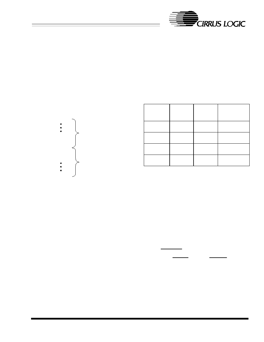
DS271PP4
73
CS8900A
Crystal LANTM ISA Ethernet Controller
CIRRUS LOGIC PRODUCT DATASHEET
Failure to observe these three rules may cause data
corruption.
4.8.1 Transferring Odd-Byte-Aligned Data
Some applications gather transmit data from more
than one section of host memory. The boundary be-
tween the various memory locations may be either
even- or odd-byte aligned. When such a boundary
is odd-byte aligned, the host should transfer the last
byte of the first block to an even address, followed
by the first byte of the second block to the follow-
ing odd address. It can then resume word transfers.
An example of this is shown in Figure 17.
4.8.2 Random Access to CS8900A Memory
The first 118 bytes of a receive frame held in the
CS8900A's on-chip memory may be randomly ac-
cessed in Memory mode. After the first 118 bytes,
only sequential access of received data is allowed.
Either byte or word access is permitted, as long as
all word accesses are executed to even-byte bound-
aries.
4.9 Memory Mode Operation
To configure the CS8900A for Memory Mode, the
PacketPage memory must be mapped into a contig-
uous 4-kbyte block of host memory. The block
must start at an X000h boundary, with the Pack-
etPage base address mapped to X000h. When the
CS8900A comes out of reset, its default configura-
tion is I/O Mode. Once Memory Mode is selected,
all of the CS8900A's registers can be accessed di-
rectly.
In Memory Mode, the CS8900A supports Standard
or Ready Bus cycles without introducing additional
wait states.
Memory moves can use MOVD (double-word
transfers) as long as the CS8900A's memory base
address is on a double word boundary. Since 286
processors don't support the MOVD instruction,
word and byte transfers must be used with a 286.
4.9.1 Accesses in Memory Mode
The CS8900A allows Read/Write access to the in-
ternal PacketPage memory, and Read access of the
optional Boot PROM. (See Section 3.7 on page 25
for a description of the optional Boot PROM.)
A memory access occurs when all of the following
are true:
�
The address on the ISA System Address bus
(SA0 - SA19) is within the Memory space
range of the CS8900A or Boot PROM.
�
The CHIPSEL input pin is low.
�
Either the MEMR pin or the MEMW pin is low.
4.9.2 Configuring the CS8900A for Memory
Mode
There are two different methods of configuring the
CS8900A for Memory Mode operation. One meth-
od allows the CS8900A's internal memory to be
mapped anywhere within the host system's 24-bit
Word Transfer
Word Transfer
Byte Transfer
Word Transfer
Word Transfer
Byte Transfer
Word Transfer
Word Transfer
First Block of Data
Second Block of Data
Figure 17. Odd-Byte Aligned Data
Description Mnemonic Read/Write
Location:
PocketPage
base +
Receive
Status
RxStatus
Read-only
0400h-0401h
Receive
Length
RxLength
Read-only
0402h-0403h
Receive
Frame
RxFrame
Read-only starts at 0404h
Transmit
Frame
TxFrame
Write-only starts at 0A00h
Table 16. Receive/Transmit Memory Locations

74
DS271PP4
CS8900A
Crystal LANTM ISA Ethernet Controller
CIRRUS LOGIC PRODUCT DATASHEET
memory space. The other method limits memory
mapping to the first 1 Mbyte of host memory space.
General Memory Mode Operation: Configuring the
CS8900A so that its internal memory can be
mapped anywhere within host Memory space re-
quires the following:
�
a simple circuit must be added to decode the
Latchable Address bus (LA20 - LA23) and the
BALE signal.
�
the host must configure the external logic with
the correct address range as follows:
1) Check to see if the INITD bit (Register 16,
SelfST, bit 7) is set, indicating that initial-
ization is complete.
2) Check to see if the ELpresent bit (Register
16, SelfST, bit B) is set. This bit indicates
that external logic for the LA bus decode is
present.
3) Set the ELSEL bit of the EEPROM Com-
mand Register to activate the ELCS pin for
use with the external decode circuit.
4) Configure the external logic serially.
�
the host must write the memory base address
into the Memory Base Address register (Pack-
etPage base + 002Ch);
�
the host must set the MemoryE bit (Register 17,
BusCTL, Bit A); and
�
the host must set the UseSA bit (Register 17,
BusCTL, Bit 9).
Limiting Memory Mode to the First 1 Mbyte of
Host Memory Space: Configuring the CS8900A so
that its internal memory can be mapped only within
the first 1 Mbyte of host memory space requires the
following:
�
the CHIPSEL pin must be tied low;
�
the ISA-bus SMEMR signal must be connected
to the MEMR pin;
�
the ISA-bus SMEMW signal must be connect-
ed to the MEMW pin;
�
the host must write the memory base address
into the Memory Base Address register (Pack-
etPage base + 002Ch);
�
the host must set the MemoryE bit (Register 17,
BusCTL, Bit A); and
�
the host must clear the UseSA bit (Register 17,
BusCTL, Bit 9).
4.9.3 Basic Memory Mode Transmit
Memory Mode transmit operations occur in the fol-
lowing order (using interrupts):
1) The host bids for storage of the frame by writ-
ing the Transmit Command to the TxCMD reg-
ister (memory base + 0144h) and the transmit
frame length to the TxLength register (memory
base + 0146h). If the transmit length is errone-
ous, the command is discarded and the Tx-
BidErr bit (Register 18, BusST, Bit 7) is set.
2) The host reads the BusST register (Register 18,
memory base + 0138h). If the Rdy4TxNOW bit
(Bit 8) is set, the frame can be written. If clear,
the host must wait for CS8900A buffer memory
to become available. If Rdy4TxiE (Register B,
BufCFG, Bit 8) is set, the host will be interrupt-
ed when Rdy4Tx (Register C, BufEvent, Bit 8)
becomes set.
3) Once the CS8900A is ready to accept the
frame, the host executes repetitive memory-to-
memory move instructions (REP MOVS) to
memory base + 0A00h to transfer the entire
frame from host memory to CS8900A memory.
For a more detailed description of transmit, see
Section 5.7 on page 98.
4.9.4 Basic Memory Mode Receive
Memory Mode receive operations occur in the fol-
lowing order (interrupts used to signal the presence
of a valid receive frame):

DS271PP4
75
CS8900A
Crystal LANTM ISA Ethernet Controller
CIRRUS LOGIC PRODUCT DATASHEET
1) A frame is received by the CS8900A, triggering
an enabled interrupt.
2) The host reads the Interrupt Status Queue
(memory base + 0120h) and is informed of the
receive frame.
3) The host reads RxStatus (memory base +
0400h) to learn the status of the receive frame.
4) The host reads RxLength (memory base +
0402h) to learn the frame's length.
5) The host reads the frame data by executing re-
petitive memory-to-memory move instructions
(REP MOVS) from memory base + 0404h to
transfer the entire frame from CS8900A mem-
ory to host memory.
For a more detailed description of receive, see
Section 5.2 on page 78.
4.9.5 Polling the CS8900A in Memory Mode
If interrupts are not used, the host can poll the
CS8900A to check if receive frames are present
and if memory space is available for transmit.
However, this is beyond the scope of this data
sheet.
4.10 I/O Space Operation
In I/O Mode, PacketPage memory is accessed
through eight 16-bit I/O ports that are mapped into
16 contiguous I/O locations in the host system's I/O
space. I/O Mode is the default configuration for the
CS8900A and is always enabled. On power up, the
default value of the I/O base address is set at 300h.
(Note that 300h is typically assigned to LAN pe-
ripherals). The I/O base address may be changed to
any available XXX0h location, either by loading
configuration data from the EEPROM, or during
system setup. Table 17 shows the CS8900A I/O
Mode mapping.
4.10.1 Receive/Transmit Data Ports 0 and 1
These two ports are used when transferring trans-
mit data to the CS8900A and receive data from the
CS8900A. Port 0 is used for 16-bit operations and
Ports 0 and 1 are used for 32-bit operations (lower-
order word in Port 0).
4.10.2 TxCMD Port
The host writes the Transmit Command (TxCMD)
to this port at the start of each transmit operation.
The Transmit Command tells the CS8900A that the
host has a frame to be transmitted, as well as how
that frame should be transmitted. This port is
mapped into PacketPage base + 0144h. See Regis-
ter 9 in Section 4.4 on page 46 for more informa-
tion.
4.10.3 TxLength Port
The length of the frame to be transmitted is written
here immediately after the Transmit Command is
written. This port is mapped into PacketPage base
+ 0146h.
4.10.4 Interrupt Status Queue Port
This port contains the current value of the Interrupt
Status Queue (ISQ). The ISQ is located at Pack-
etPage base + 0120h. For a more detailed descrip-
tion of the ISQ, see Section 5.1 on page 78.
4.10.5 PacketPage Pointer Port
The PacketPage Pointer Port is written whenever
the host wishes to access any of the CS8900A's in-
ternal registers. The first 12 bits (bits 0 through B)
provide the internal address of the target register to
be accessed during the current operation. The next
Offset
Type
Description
0000h Read/Write Receive/Transmit Data (Port 0)
0002h Read/Write Receive/Transmit Data (Port 1)
Table 17. I/O Mode Mapping
0004h
Write-only
TxCMD (Transmit Command)
0006h
Write-only
TxLength (Transmit Length)
0008h
Read-only
Interrupt Status Queue
000Ah Read/Write
PacketPage Pointer
000Ch Read/Write
PacketPage Data (Port 0)
000Eh Read/Write
PacketPage Data (Port 1)
Offset
Type
Description
Table 17. I/O Mode Mapping

76
DS271PP4
CS8900A
Crystal LANTM ISA Ethernet Controller
CIRRUS LOGIC PRODUCT DATASHEET
three bits (C, D, and E) are read-only and will al-
ways read as 011b. Any convenient value may be
written to these bits when writing to the PacketPage
Pointer Port. The last bit (Bit F) indicates whether
or not the PacketPage Pointer should be auto-incre-
mented to the next word location. Figure 18 shows
the structure of the PacketPage Pointer.
4.10.6 PacketPage Data Ports 0 and 1
The PacketPage Data Ports are used to transfer data
to and from any of the CS8900A's internal regis-
ters. Port 0 is used for 16-bit operations and Port 0
and 1 are used for 32-bit operations (lower-order
word in Port 0).
4.10.7 I/O Mode Operation
For an I/O Read or Write operation, the AEN pin
must be low, and the 16-bit I/O address on the ISA
System Address bus (SA0 - SA15) must match the
address space of the CS8900A. For a Read, the IOR
pin must be low, and for a Write, the IOW pin must
be low.
Note: The ISA Latchable Address Bus (LA17 -
LA23) is not needed for applications that use only
I/O Mode and Receive DMA operation.
4.10.8 Basic I/O Mode Transmit
I/O Mode transmit operations occur in the follow-
ing order (using interrupts):
1) The host bids for storage of the frame by writ-
ing the Transmit Command to the TxCMD Port
(I/O base + 0004h) and the transmit frame
length to the TxLength Port (I/O base + 0006h).
2) The host reads the BusST register (Register 18)
to see if the Rdy4TxNOW bit (Bit 8) is set. To
read the BusST register, the host must first set
the PacketPage Pointer at the correct location
by writing 0138h to the PacketPage Pointer
Port (I/O base + 000Ah). It can then read the
BusST register from the PacketPage Data Port
(I/O base + 000Ch). If Rdy4TxNOW is set, the
frame can be written. If clear, the host must
wait for CS8900A buffer memory to become
available. If Rdy4TxiE (Register B, BufCFG,
Bit 8) is set, the host will be interrupted when
Rdy4Tx (Register C, BufEvent, Bit 8) becomes
set. If the TxBidErr bit (Register 18, BusST, Bit
7) is set, the transmit length is not valid.
3) Once the CS8900A is ready to accept the
frame, the host executes repetitive write in-
structions (REP OUT) to the Receive/Transmit
Data Port (I/O base + 0000h) to transfer the en-
tire frame from host memory to CS8900A
memory.
For a more detailed description of transmit, see
Section 5.7 on page 98.
4.10.9 Basic I/O Mode Receive
I/O Mode receive operations occur in the following
order (In this example, interrupts are enabled to
signal the presence of a valid receive frame):
1) A frame is received by the CS8900A, triggering
an enabled interrupt.
2) The host reads the Interrupt Status Queue Port
(I/O base + 0008h) and is informed of the re-
ceive frame.
3) The host reads the frame data by executing re-
petitive read instructions (REP IN) from the
Receive/Transmit Data Port (I/O base + 0000h)
to transfer the frame from CS8900A memory to
1 0
3 2
5
4
7 6
PacketPage Register Address
9
8
B A
D C
F E
I/O base + 000Bh
I/O base + 000Ah
Bit F: 0 = Pointer remains fixed
1 = Auto-Increments to next word location
Figure 18. PacketPage Pointer

DS271PP4
77
CS8900A
Crystal LANTM ISA Ethernet Controller
CIRRUS LOGIC PRODUCT DATASHEET
host memory. Preceding the frame data are the
contents of the RxStatus register (PacketPage
base + 0400h) and the RxLength register (Pack-
etPage base + 0402h).
For a more detailed description of receive, see
Section 5.2 on page 78.
4.10.10 Accessing Internal Registers
To access any of the CS8900A's internal registers
in I/O Mode, the host must first setup the Pack-
etPage Pointer. It does this by writing the Pack-
etPage address of the target register to the
PacketPage Pointer Port (I/O base + 000Ah). The
contents of the target register is then mapped into
the PacketPage Data Port (I/O base + 000Ch).
If the host needs to access a sequential block of reg-
isters, the MSB of the PacketPage address of the
first word to be accessed should be set to "1". The
PacketPage Pointer will then move to the next word
location automatically, eliminating the need to set-
up the PacketPage Pointer between successive ac-
cesses (see Figure 18).
4.10.11 Polling the CS8900A in I/O Mode
If interrupts are not used, the host can poll the
CS8900A to check if receive frames are present
and if memory space is available for transmit.

78
DS271PP4
CS8900A
Crystal LANTM ISA Ethernet Controller
CIRRUS LOGIC PRODUCT DATASHEET
5.0 OPERATION
5.1 Managing Interrupts and Servicing the
Interrupt Status Queue
The Interrupt Status Queue (ISQ) is used by the
CS8900A to communicate Event reports to the host
processor. Whenever an event occurs that triggers
an enabled interrupt, the CS8900A sets the appro-
priate bit(s) in one of five registers, maps the con-
tents of that register to the ISQ, and drives the
selected interrupt request pin high (if an earlier in-
terrupt is waiting in the queue, the interrupt request
pin will already be high). When the host services
the interrupt, it must first read the ISQ to learn the
nature of the interrupt. It can then process the inter-
rupt (the first read to the ISQ causes the interrupt
request pin to go low.)
Three of the registers mapped to the ISQ are event
registers: RxEvent (Register 4), TxEvent (Register
8), and BufEvent (Register C). The other two reg-
isters are counter-overflow reports: RxMISS (Reg-
ister 10) and TxCOL (Register 12). There may be
more than one RxEvent report and/or more than
one TxEvent report in the ISQ at a time. However,
there may be only one BufEvent report, one Rx-
MISS report and one TxCOL report in the ISQ at a
time.
Event reports stored in the ISQ are read out in the
order of priority, with RxEvent first, followed by
TxEvent, BufEvent, RxMiss, and then TxCOL.
The host only needs to read from one location to get
the interrupt currently at the front of the queue. In
Memory Mode, the ISQ is located at PacketPage
base + 0120h. In I/O Mode, it is located at I/O base
+ 0008h. Each time the host reads the ISQ, the bits
in the corresponding register are cleared and the
next report in the queue moves to the front.
When the host starts reading the ISQ, it must read
and process all Event reports in the queue. A read-
out of a null word (0000h) indicates that all inter-
rupts have been read.
The ISQ is read as a 16-bit word. The lower six bits
(0 through 5) contain the register number (4, 8, C,
10, or 12). The upper ten bits (6 through F) contain
the register contents. The host must always read the
entire 16-bit word.
The active interrupt pin (INTRQx) is selected via
the Interrupt Number register (PacketPage base +
22h). As an additional option, all of the interrupt
pins can be 3-Stated using the same register. see
Section 4.3 on page 41.
An event triggers an interrupt only when the En-
ableIRQ bit of the Bus Control register (bit F of
register 17) is set. After the CS8900A has generat-
ed an interrupt, the first read of the ISQ makes the
INTRQ output pin go low (inactive). INTRQ re-
mains low until the null word (0000h) is read from
the ISQ, or for 1.6us, whichever is longer.
5.2 Basic Receive Operation
5.2.0.1 Overview
Once an incoming packet has passed through the
analog front end and Manchester decoder, it goes
through the following three-step receive process:
1) Pre-Processing
2) Temporary Buffering
3) Transfer to Host
Figure 20 shows the steps in frame reception.
As shown in the figure, all receive frames go
through the same pre-processing and temporary
buffering phases, regardless of transfer method
Once a frame has been pre-processed and buffered,
it can be accessed by the host in either Memory or
I/O space. In addition, the CS8900A can transfer
receive frames to host memory via host DMA. This
section describes receive frame pre-processing and
Memory and I/O space receive operation.
Section 5.4 on page 89 through Section 5.5 on
page 92 describe DMA operation.

DS271PP4
79
CS8900A
Crystal LANTM ISA Ethernet Controller
CIRRUS LOGIC PRODUCT DATASHEET
An enabled interrupt occurs.
The selected interrupt
request pin is driven high
(active) if not already high.
ISQ = 0000h?
Yes
The host reads the ISQ.
The selected interrupt
request pin is driven low.
No
Process applicable
RxEvent bits: Extradata,
Runt, CRCerror, RxOK.
Process applicable
TxEvent bits: 16coll, Jabber,
Out-of-window, TxOK.
Process applicable BufEvent
bits: RxDest, Rx128, RxMiss,
TxUnderrun, Rdy4Tx,
RxDMAFrame, SWint.
Process RxMISS counter.
Process TxCOL counter.
Which
Event
report
type?
RxEvent
TxEvent
BufEvent
RxMISS
TxCOL
None of the above
Service
Default
EXIT.
Interrupts
re-enabled.
(Interrupts
will be
disabled
for at least
1.6 us.)
Figure 19. Interrupt Status Queue

80
DS271PP4
CS8900A
Crystal LANTM ISA Ethernet Controller
CIRRUS LOGIC PRODUCT DATASHEET
5.2.1 Terminology: Packet, Frame, and Transfer
The terms Packet, Frame, and Transfer are used ex-
tensively in the following sections. They are de-
fined below for clarity:
5.2.1.1 Packet
The term "packet" refers to the entire serial string
of bits transmitted over an Ethernet network. This
includes the preamble, Start-of-Frame Delimiter
(SFD), Destination Address (DA), Source Address
(SA), Length field, Data field, pad bits (if neces-
sary), and Frame Check Sequence (FCS, also
called CRC). Figure 9 shows the format of a pack-
et.
5.2.1.2 Frame
The term "frame" refers to the portion of a packet
from the DA to the FCS. This includes the Destina-
tion Address (DA), Source Address (SA), Length
field, Data field, pad bits (if necessary), and Frame
Check Sequence (FCS, also called CRC). Figure 9
shows the format of a frame. The term "frame data"
refers to all the data from the DA to the FCS that is
to be transmitted, or that has been received.
5.2.1.3 Transfer
The term "transfer" refers to moving data across the
ISA bus, to and from the CS8900A. During receive
operations, only frame data are transferred from the
CS8900A to the host (the preamble and SFD are
stripped off by the CS8900A's MAC engine). The
FCS may or may not be transferred, depending on
the configuration. All transfers to and from the
CS8900A are counted in bytes, but may be padded
for double word alignment.
5.2.2 Receive Configuration
After each reset, the CS8900A must be configured
for receive operation. This can be done automati-
cally using an attached EEPROM or by writing
configuration commands to the CS8900A's internal
registers (see Section 3.4 on page 20). The items
that must be configured include:
�
which physical interface to use;
�
which types of frames to accept;
�
which receive events cause interrupts; and,
�
how received frames are transferred.
5.2.2.1 Configuring the Physical Interface
Configuring the physical interface consists of de-
termining which Ethernet interface should be ac-
tive, and enabling the receive logic for serial
reception. This is done via the LineCTL register
(Register 13) and is described in Table18.
5.2.2.2 Choosing which Frame Types to Accept
The RxCTL register (Register 5) is used to deter-
mine which frame types will be accepted by the
CS8900A (a receive frame is said to be "accepted"
when the frame is buffered, either on chip or in host
Yes
No
Use
DMA?
Frame Held
On Chip
Frame DMAed
to Host Memory
Host Reads
Frame from
Host Memory
Frame Pre-
Processed
Frame
Temporarily
Buffered
Packet Received
Preamble and
Start-of-Frame
Delimiter Removed
Host Reads
Frame from
CS8900A Memory
Figure 20. Frame Reception

DS271PP4
81
CS8900A
Crystal LANTM ISA Ethernet Controller
CIRRUS LOGIC PRODUCT DATASHEET
memory via DMA). Table 19 describes the config-
uration bits in this register. Refer to Section 5.3 on
page 86 for a detailed description of Destination
Address filtering.
5.2.2.3 Selecting which Events Cause Interrupts
The RxCFG register (Register 3) and the BufCFG
register (Register B) are used to determine which
receive events will cause interrupts to the host pro-
cessor. Table 21 describes the interrupt enable (iE)
bits in these registers.
5.2.2.4 Choosing How to Transfer Frames
The RxCFG register (Register 3) and the BusCTL
register (Register 17) are used to determine how
frames will be transferred to host memory, as de-
scribed in Table 22.
Register 13, LineCTL
Bit Bit
Name
Operation
6
SerRxON
When set, reception enabled.
8
AUIonly
When set, AUI selected (takes
precedence over AutoAUI/10BT).
9
AutoAUI/10BT When set, automatic interface
selection enabled. When both bits
8 and 9 are clear, 10BASE-T
selected.
E
LoRx Squelch When set, receiver squelch level
reduced by approximately 6 dB.
Table 18. Physical Interface Configuration
Register 5, RxCTL
Bit Bit
Name
Operation
6
IAHashA When set, Individual Address frames
that pass the hash filter are
accepted*.
7
Promis
cuousA
When set, all frames are accepted*.
8
RxOKA
When set, frames with valid length
and CRC and that pass the DA filter
are accepted.
9
MulticastA When set, Multicast frames that pass
the hash filter are accepted*.
A
IndividualA When set, frames with DA that
matches the IA at PacketPage base
+ 0158h are accepted*.
B
Broad-
castA
When set, all broadcast frames are
accepted*.
C
CRCerrorA When set, frames with bad CRC that
pass the DA filter are accepted.
D
RuntA
When set, frames shorter than 64
bytes that pass the DA filter are
accepted.
E
ExtradataA When set, frames longer than 1518
bytes that pass the DA filter are
accepted (only the first 1518 bytes
are buffered).
* Must also meet the criteria programmed into bits 8, C, D,
and E.
Table 19. Frame Acceptance Criteria
Register 3, RxCFG
Bit Bit
Name
Operation
8
RxOKiE
When set, there is an interrupt if a
frame is received with valid length
and CRC*.
C CRCerroriE When set, there is an interrupt if a
frame is received with bad CRC*.
D
RuntiE
When set, there is an interrupt if a
frame is received that is shorter than
64 bytes*.
E
ExtradataiE When set, there is an interrupt if a
frame is received that is longer than
1518 bytes*.
* Must also pass the DA filter before there is an interrupt.
Table 20.
Register B, BufCFG
Bit Bit
Name
Operation
7
RxDMAiE
When set, there is an interrupt if
one or more frames are trans-
ferred via DMA.
A
RxMissiE
When set, there is an interrupt if a
frame is missed due to insufficient
receive buffer space.
B
Rx128iE
When set, there is an interrupt
after the first 128 bytes of receive
data have been buffered.
D
MissOvfloiE When set, there is an interrupt if
the RxMISS counter overflows.
F
RxDestiE
When set, there is an interrupt
after the DA of an incoming frame
has been buffered.
Table 21. Registers 3 and B Interrupt Configuration
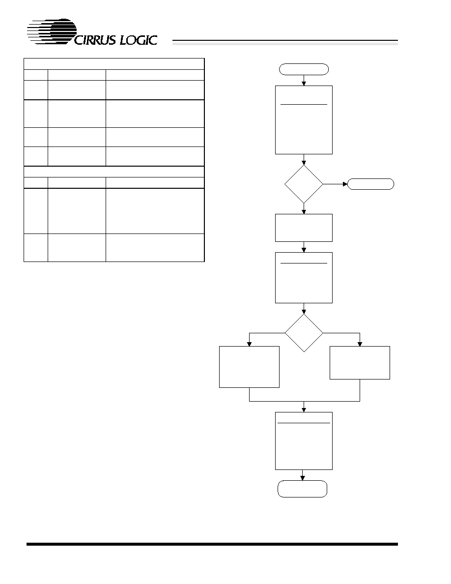
82
DS271PP4
CS8900A
Crystal LANTM ISA Ethernet Controller
CIRRUS LOGIC PRODUCT DATASHEET
5.2.3 Receive Frame Pre-Processing
The CS8900A pre-processes all receive frames us-
ing a four step process:
1) Destination Address filtering;
2) Early Interrupt Generation;
3) Acceptance filtering; and,
4) Normal Interrupt Generation.
Figure 21 provides a diagram of frame pre-process-
ing.
5.2.3.1 Destination Address Filtering
All incoming frames are passed through the Desti-
nation Address filter (DA filter). If the frame's DA
passes the DA filter, the frame is passed on for fur-
ther pre-processing. If it fails the DA filter, the
frame is discarded. See Section 5.3 on page 86 for
a more detailed description of DA filtering.
Register 3, RxCFG
Bit Bit
Name
Operation
7
StreamE
When set, Stream Transfer
enabled.
9
RxDMAonly
When set, DMA slave opera-
tion used for all receive
frames.
A
AutoRX DMAE When set, Auto-Switch DMA
enabled.
B
BufferCRC
When set, the received CRC
is buffered.
Register 17, BusCTL
Bit
Bit Name
Operation
B
DMABurst
When set, DMA operations
hold the bus for up to approx-
imately 28 �s. When clear,
DMA operations are continu-
ous.
D
RxDMAsize
When set, DMA buffer size is
64 Kbytes. When clear, DMA
buffer size is 16 Kbytes.
Table 22. Receive Frame Pre-Processing
Pass
DA Filter?
Discard Frame
Destination
Address Filter
Check:
- PromiscuousA?
- IAHashA?
- MulticastA?
- IndividualA?
- BroadcastA?
Receive Frame
Yes
No
Yes
No
Generate Interrupts
Check:
- RxOKiE?
- ExtradataiE?
- CRCerroriE?
- RuntiE?
- RxDMAiE?
Pre-Processing
Complete
Generate Early
Interrupts if Enabled
(see next figure)
Acceptance Filter
Check:
- RxOKA?
- ExtradataA?
- RuntA?
- CRCerrorA?
Status of receive
frame reported in
RxEvent register,
frame discarded.
Status of receive
frame reported in
RxEvent register,
frame accepted
into on-chip RAM
Pass
Accept.
Filter?
Figure 21. Receive Frame Pre-Processing

DS271PP4
83
CS8900A
Crystal LANTM ISA Ethernet Controller
CIRRUS LOGIC PRODUCT DATASHEET
5.2.3.2 Early Interrupt Generation
The CS8900A support the following two early in-
terrupts that can be used to inform the host that a
frame is being received:
�
RxDest: The RxDest bit (Register C, BufEvent,
Bit F) is set as soon as the Destination Address
(DA) of the incoming frame passes the DA fil-
ter. If the RxDestiE bit (Register B, BufCFG,
bit F) is set, the CS8900A generates a corre-
sponding interrupt. Once RxDest is set, the host
is allowed to read the incoming frame's DA (the
first 6 bytes of the frame).
�
Rx128: The Rx128 bit (Register C, BufEvent,
Bit B) is set as soon as the first 128 bytes of the
incoming frame have been received. If the
Rx128iE bit (Register B, BufCFG, bit B) is set,
the CS8900A generates a corresponding inter-
rupt. Once the Rx128 bit is set, the RxDest bit
is cleared and the host is allowed to read the
first 128 bytes of the incoming frame. The
Rx128 bit is cleared by the host reading the
BufEvent register (either directly or through the
Interrupt Status Queue) or by the CS8900A de-
tecting the incoming frame's End-of-Frame
(EOF) sequence.
Like all Event bits, RxDest and Rx128 are set by
the CS8900A whenever the appropriate event oc-
curs. Unlike other Event bits, RxDest and Rx128
may be cleared by the CS8900A without host inter-
vention. All other event bits are cleared only by the
host reading the appropriate event register, either
directly or through the Interrupt Status Queue
(ISQ). (RxDest and Rx128 can also be cleared by
the host reading the BufEvent register, either di-
rectly or through the Interrupt Status Queue). Fig-
ure 22 provides a diagram of the Early Interrupt
process.
5.2.3.3 Acceptance Filtering
The third step of pre-processing is to determine
whether or not to accept the frame by comparing
the frame with the criteria programmed into the Rx-
CTL register (Register 5). If the receive frame
passes the Acceptance filter, the frame is buffered,
either on chip or in host memory via DMA. If the
frame fails the Acceptance filter, it is discarded.
The results of the Acceptance filter are reported in
the RxEvent register (Register 4).
5.2.3.4 Normal Interrupt Generation
The final step of pre-processing is to generate any
enabled interrupts that are triggered by the incom-
ing frame. Interrupt generation occurs when the en-
tire frame has been buffered (up to the first 1518
bytes). For more information about interrupt gener-
ation, see Section 5.1 on page 78.
5.2.4 Held vs. DMAed Receive Frames
All accepted frames are either held in on-chip
RAM until processed by the host, or stored in host
memory via DMA. A receive frame that is held in
on-chip RAM is referred to as a held receive frame.
A frame that is stored in host memory via DMA is
a DMAed receive frame. This section describes
buffering and transferring held receive frames.
Section 5.4 on page 89 through Section 5.6 on
page 95 describe DMAed receive frames.
5.2.5 Buffering Held Receive Frames
If space is available, an incoming frame will be
temporarily stored in on-chip RAM, where it
awaits processing by the host. Although this re-
ceive frame now occupies on-chip memory, the
CS8900A does not commit the memory space to it
until one of the following two conditions is true:
1) The entire frame has been received and the host
has learned about the frame by reading the Rx-
Event register (Register 4), either directly or
through the ISQ.
Or:
2) The frame has been partially received, causing
either the RxDest bit (Register C, BufEvent, Bit
F) or the Rx128 bit (Register C, BufEvent, Bit
B) to become set, and the host has learned about

84
DS271PP4
CS8900A
Crystal LANTM ISA Ethernet Controller
CIRRUS LOGIC PRODUCT DATASHEET
EOF
Received?
128 bytes
Received?
EOF
Received?
64 bytes
Received?
EOF
Received?
Receive Frame
RxDest cleared
and Runt set.
If RuntA is set,
frame accepted and
Host may read frame.
RxDest cleared and
RxOK or CRCerror
set, as appropriate.
If RxOKA or CRCerrorA
is set, frame accepted and
Host may read frame.
Rx128 cleared and
RxOK, CRCerror or
Extradata set, as
appropriate. If ExtradataA,
RxOKA or CRCerrorA is
set, frame is accepted and
Host may read frame.
DA Filter
Passed?
Yes
No
Yes
No
No
Yes
Yes
No
No
Yes
Rx128 set and
RxDest cleared.
Host may read first
128 received bytes.
Yes
No
Discard Frame
RxDest set.
Host may read the DA
(first 6 received bytes).
Figure 22. Early Interrupt Generation

DS271PP4
85
CS8900A
Crystal LANTM ISA Ethernet Controller
CIRRUS LOGIC PRODUCT DATASHEET
the receive frame by reading the BufEvent reg-
ister (Register C), either directly or through the
ISQ.
When the CS8900A commits buffer space to a par-
ticular held receive frame (termed a committed re-
ceived frame), no data from subsequent frames can
be written to that buffer space until the frame is
freed from commitment. (The committed received
frame may or may not have been received error
free.)
A received frame is freed from commitment by any
one of the following conditions:
1) The host reads the entire frame sequentially in
the order that it was received (first byte in, first
byte out).
Or:
2) The host reads part or none of the frame, and
then issues a Skip command by setting the
Skip_1 bit (Register 3, RxCFG, bit 6).
Or:
3) The host reads part of the frame and then reads
the RxEvent register (Register 5), either direct-
ly or through the ISQ, and learns of another re-
ceive frame. This condition is called an
"implied Skip". Ensure that the host does not do
"implied skips."
Both early interrupts are disabled whenever there is
a committed receive frame waiting to be processed
by the host.
5.2.6 Transferring Held Receive Frames
The host can read-out held receive frames in Mem-
ory or I/O space. To transfer frames in Memory
space, the host executes repetitive Move instruc-
tions (REP MOVS) from PacketPage base +
0404h. To transfer frames in I/O space, the host ex-
ecutes repetitive In instructions (REP IN) from I/O
base + 0000h, with status and length preceding the
frame.
There are three possible ways that the host can
learn the status of a particular frame. It can:
1) Read the Interrupt Status Queue;
2) Read the RxEvent register directly (Register4);
or
3) Read the RxStatus register (PacketPage base +
0400h).
5.2.7 Receive Frame Visibility
Only one receive frame is visible to the host at a
time. The receive frame's status can be read from
the RxStatus register (PacketPage base + 0400h),
and its length can be read from the RxLength reg-
ister (PacketPage base + 0402h). For more infor-
mation about Memory space operation, see
Section 4.9 on page 73. For more information
about I/O space operation, see Section 4.10 on
page 75.
5.2.8 Example of Memory Mode Receive Opera-
tion
A common length for short frames is 64 bytes, in-
cluding the 4-byte CRC. Suppose that such a frame
has been received with the CS8900A configured as
follows:
�
The BufferCRC bit (Register 3, RxCFG, Bit B)
is set causing the 4-byte CRC to be buffered
with the rest of the receive data.
�
The RxOKA bit (Register 5, RxCTL, Bit 8) is
set, causing the CS8900A to accept good
frames (a good frame is one with legal length
and valid CRC).
�
The RxOKiE bit (Register 3, RxCFG, Bit 8) is
set, causing an interrupt to be generated when-
ever a good frame is received.
Then the transfer to the host would proceed as fol-
lows:
1) The CS8900A generates an RxOK interrupt to
the host to signal the arrival of a good frame.
2) The host reads the ISQ (PacketPage base +

86
DS271PP4
CS8900A
Crystal LANTM ISA Ethernet Controller
CIRRUS LOGIC PRODUCT DATASHEET
0120h) to assess the status of the receive frame
and sees the contents of the RxEvent register
(Register 4) with the RxOK bit (Bit 8) set.
3) The host reads the receive frame's length from
the RxLength register (PacketPage base +
0402h).
4) The host reads the frame data by executing 32
consecutive MOV instructions starting with
PacketPage base + 0404h.
The memory map of the 64-byte frame is given in
Table 23.
5.2.9 Receive Frame Byte Counter
The receive frame byte counter describes the num-
ber of bytes received for the current frame. The
counter is incremented in real time as bytes are re-
ceived from the Ethernet. The byte counter can be
used by the driver to determine how many bytes are
available for reading out of the CS8900A. Maxi-
mum Ethernet throughput can be achieved by using
I/O or memory modes, and by dedicating the CPU
to reading this counter, and using the count to read
the frame out of the CS8900A at the same time it is
being received by the CS8900A from the Ethernet
(parallel frame-reception and frame-read-out
tasks).
The byte count register resides at PacketPage base
+ 50h.
Following an RxDest or Rx128 interrupt the regis-
ter contains the number of bytes which are avail-
able to be read by the CPU. When the end of frame
is reached, the count contains the final count value
for the frame, including the allowance for the Buff-
erCRC option. When this final count is read by the
CPU the count register is set to zero. Therefore to
read a complete frame using the byte count register,
the register can be read and the data moved until a
count of zero is detected. Then the RxEvent regis-
ter can be read to determine the final frame status.
The sequence is as follows:
1) At the start of a frame, the byte counter matches
the incoming character counter. The byte
counter will have an even value prior to the end
of the frame.
2) At the end of the frame, the final count, includ-
ing the allowance for the CRC (if the Buffer-
CRC option is enabled), is held until the byte
counter is read.
3) When a read of the byte counter returns a count
of zero, the previous count was the final count.
The count may now have an odd value.
4) RxEvent should be read to obtain a final status
of the frame, followed by a Skip command to
complete the operation.
Note that all RxEvent's should be processed before
using the byte counter. The byte counter should be
used following a BufEvent when RxDest or Rx128
interrupts are enabled.
5.3 Receive Frame Address Filtering
The CS8900A is equipped with a Destination Ad-
dress (DA) filter used to determine which receive
frames will be accepted. (A receive frame is said to
be "accepted" by the CS8900A when the frame
data are placed in either on-chip memory, or in host
Memory Space
Word Offset
Description of Data Stored in On-
chip RAM
0400h
RxStatus Register (the host may
skip reading 0400h since RxEvent
was read from the ISQ.)
0402h
RxLength Register (In this example,
the length is 40h bytes. The frame
starts at 0404h, and runs through
0443h.)
0404h to 0409h 6-byte Source Address.
040Ah to 040Fh 6-byte Destination Address.
0410h to 0411h 2-byte Length or Type Field.
0412h to 043Fh 46 bytes of data.
0440h
CRC, bytes 1 and 2
0442h
CRC, bytes 3 and 4
Table 23. Example Memory Map
DS271PP4
87
CS8900A
Crystal LANTM ISA Ethernet Controller
CIRRUS LOGIC PRODUCT DATASHEET
memory by DMA). The DA filter can be config-
ured to accept the following frame types:
5.3.0.1 Individual Address Frames
For all Individual Address frames, the first bit of
the DA is a "0" (DA[0] = 0), indicating that the ad-
dress is a Physical Address. The address filter ac-
cepts Individual Address frames whose DA
matches the Individual Address (IA) stored at
PacketPage base + 0158h, or whose hash-filtered
DA matches one of the bits programmed into the
Logical Address Filter (the hash filter is described
later in this section).
5.3.0.2 Multicast Frames
For Multicast Frames, the first bit of the DA is a "1"
(DA[0] = 1), indicating that the frame is a Logical
Address. The address filter accepts Multicast
frames whose hash-filtered DA matches one of the
bits programmed into the Logical Address Filter
(the hash filter is described later is this section). As
shown in Table 25, Broadcast Frames can be ac-
cepted as Multicast frames under a very specific set
of conditions.
5.3.0.3 Broadcast Frames
Frames with DA equal to FFFF FFFF FFFFh are
broadcast frames. In addition, the CS8900A can be
configured for Promiscuous Mode, in which case it
will accept all receive frames, irrespective of DA.
5.3.1 Configuring the Destination Address Filter
The DA filter is configured by programming five
DA filter bits in the RxCTL register (Register 5):
IAHashA, PromiscuousA, MulticastA, Individua-
lA, and BroadcastA. Four of these bits are associat-
ed with four status bits in the RxEvent register
(Register 4): IAHash, Hashed, IndividualAdr, and
Broadcast. The RxEvent register reports the results
of the DA filter for a given receive frame. The bits
associated with DA filtering are summarized be-
low:
The IAHashA, MulticastA, IndividualA, and
BroadcastA bits are used independently. As a re-
sult, many DA filter combinations are possible. For
example, if MulticastA and IndividualA are set,
then all frames that are either Multicast or Individ-
ual Address frames are accepted. The Promiscu-
ousA bit, when set, overrides the other four DA
bits, and allows all valid frames to be accepted. Ta-
ble 24 summarizes the configuration options avail-
able for DA filtering.
Bit #
RxCTL
Register 5
RxEvent
Register 4
6
IAHashA
IAHash
(used only if IAHashA = 1)
7
PromiscuousA
9
MulticastA
Hashed
A
IndividualA
IndividualAdr
(used only if IndividualA = 1)
B
BroadcastA
Broadcast
(used only if BroadcastA = 1)
IAHashA
PromiscuousA
MulticastA
IndividualA
BroadcastA
Frames Accepted
0
0
0
1
0
Individual Address frames with
DA matching the IA at Pack-
etPage base + 0158h
1
0
0
0
0
Individual Address frames with
DA that pass the hash filter
(DA[0] must be "0")
0
0
1
0
0
Multicast frames with DA that
pass the hash filter (DA[0] must
be "1")
0
0
0
0
1
Broadcast frames
X
1
X
X
X
All frames
Table 24. DA Filtering Options
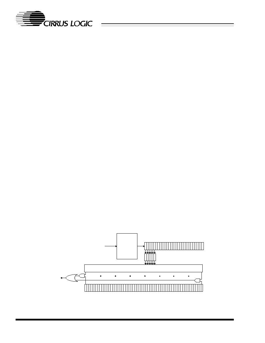
88
DS271PP4
CS8900A
Crystal LANTM ISA Ethernet Controller
CIRRUS LOGIC PRODUCT DATASHEET
It may become necessary for the host to change the
Destination Address (DA) filter criteria without re-
setting the CS8900A. This can be done as follows:
1) Clear SerRxON (Register 13, LineCTL, Bit 6)
to prevent any additional receive frames while
the filter is being changed.
2) Modify the DA filter bits (B, A, 9, 7, and 6) in
the RxCTL register. Modify the Logical Ad-
dress Filter at PacketPage base + 0150h, if nec-
essary.
Modify the Individual Address at
PacketPage base + 0158h, if necessary.
3) Set SerRxON to re-enable the receiver.
Because the receiver has been disabled, the
CS8900A will ignore frames while the host is
changing the DA filter.
5.3.2 Hash Filter
The hash filter is used to help determine which
Multicast frames and which Individual Address
frames should be accepted by the CS8900A.
5.3.2.1 Hash Filter Operation
See Figure 23. The DA of the incoming frame is
passed through the CRC logic, generating a 32-bit
CRC value. The six most-significant bits of the
CRC are latched into the 6-bit hash register (HR).
The contents of the HR are passed through a 6-to-
64-bit decoder, asserting one of the decoder's out-
puts. The asserted output is compared with a corre-
sponding bit in the 64-bit Logical Address Filter,
located at PacketPage base + 0150h. If the decoder
output and the Logical Address Filter bit match, the
frame passes the hash filter and the Hashed bit
(Register 4, RxEvent, Bit 9) is set. If the two do not
match, the frame fails the filter and the Hashed bit
is clear.
Whenever the hash filter is passed by a "good"
frame, the RxOK bit (Register 4, RxEvent, Bit 8) is
set and the bits in the HR are mapped to the Hash
Table Index bits (Register 4, RxEvent, Bits A
through F).
5.3.3 Broadcast Frame Hashing Exception
Table 25 describes in detail the content of the Rx-
Event register for each output of the hash and ad-
dress filters, and describes an exception to normal
processing. That exception can occur when the
hash-filter Broadcast address matches a bit in the
Logical Address Filter. To properly account for this
exception, the software driver should use the fol-
lowing test to determine if the RxEvent register
contains a normal RxEvent (meaning bits E-A are
used for Extra data, Runt, CRC Error, Broadcast
and IndividualAdr) or a hash-table RxEvent (mean-
ing bits F-A contain the Hash Table Index).
If bit Hashed =0, or bit RxOK=0, or (bits F-A = 02h
and the destination address is all ones) then Rx-
Event contains a normal RxEvent, else RxEvent
contained a hash RxEvent.
64-bit Logical Address Filter (LAF)
Written into PacketPage base + 150h
6-to-64 decoder
1
64
CS8900A
CRC
Logic
Destination Address (DA)
from incoming frame
32-bit CRC value
(MSB)
(LSB)
6-bit Hash Register (HR)
[Hash Table Index]
64-input
OR gate
to
Hashed
bit
Figure 23. Hash Filter Operation

DS271PP4
89
CS8900A
Crystal LANTM ISA Ethernet Controller
CIRRUS LOGIC PRODUCT DATASHEET
5.4 Receive DMA
5.4.1 Overview
The CS8900A supports a direct interface to the host
DMA controller allowing it to transfer receive
frames to host memory via slave DMA. The DMA
option applies only to receive frames, and not
transmit operation. The CS8900A offers three pos-
sible Receive DMA modes:
1) Receive-DMA-only mode: All receive frames
are transferred via DMA.
2) Auto-Switch DMA: DMA is used only when
needed to help prevent missed frames.
3) StreamTransfer: DMA is used to minimize the
number of interrupts to the host.
This section provides a description of Receive-
DMA-only mode. Section 5.5 on page 92 describes
Auto-Switch DMA and Section 5.6 on page 95 de-
scribes StreamTransfer.
5.4.2 Configuring the CS8900A for DMA Opera-
tion
The CS8900A interfaces to the host DMA control-
ler through one pair of the DMA request/acknowl-
edge pins (see Section 3.2 on page 17 for a
description of the CS8900A's DMA interface).
Four 16-bit registers are used for DMA operation.
These are described in Table 26.
Receive-DMA-only mode is enabled by setting the
RxDMAonly bit (Register 3, RxCFG, Bit 9).
Note: If the RxDMAonly bit and the AutoRxD-
MAE bit (Register 3, RxCFG, Bit A) are both set,
then RxDMAonly takes precedence, and the
CS8900A is in DMA mode for all receive frames.
5.4.3 DMA Receive Buffer Size
In receive DMA mode, the CS8900A stores re-
ceived frames (along with their status and length)
in a circular buffer located in host memory space.
Address
Type of
Received
Frame
Erred
Frame?
Passes
Hash
Filter?
Contents of RxEvent
Bits F-A
Bit 9
Hashed
Bit 8
RxOK
Bit 6
IAHash
Individual
Address
no
yes
Hash Table Index
1
1
1
no
no
ExtraData Runt CRC Error Broadcast Individual Adr
0
1
0
yes
don't care ExtraData Runt CRC Error Broadcast Individual Adr
0
0
0
Multicast
Address
no
yes
Hash table index
1
1
0
no
no
ExtraData Runt CRC Error Broadcast Individual Adr
0
1
0
yes
don't care ExtraData Runt CRC Error Broadcast Individual Adr
0
0
0
Broad-
cast
Address
no
yes
(Note 6)
ExtraData Runt CRC Error Broadcast Individual Adr
1
1
0
(actual value X00010)
no
yes
(Note 7)
ExtraData Runt CRC Error Broadcast Individual Adr
0
1
0
no
no
ExtraData Runt CRC Error Broadcast Individual Adr
0
1
0
yes
don't care ExtraData Runt CRC Error Broadcast Individual Adr
0
0
0
Notes: 6. Broadcast frames are accepted as Multicast frames if and only if all the following conditions are met
simultaneously:
a) the Logical Address Filter is programmed as: (MSB) 0000 8000 0000 0000h (LSB). Note that this
LAF value corresponds to a Multicast Addresses of both all 1s and 03-00-00-00-00-01.
b) the Rx Control Register (register 5) is programmed to accept IndividualA, MulticastA, RxOK-only,
and the following address filters were enabled: IAHashA and BroadcastA.
7. NOT (Note 1).
Table 25. Contents of RxEvent Upon Various Conditions
90
DS271PP4
CS8900A
Crystal LANTM ISA Ethernet Controller
CIRRUS LOGIC PRODUCT DATASHEET
The size of the circular buffer is determined by the
RxDMAsize bit (Register 17, BusCTL, Bit D).
When RxDMAsize is clear, the buffer size is 16
Kbytes. When RxDMAsize is set, the buffer is 64
Kbytes. It is the host's task to locate and keep track
of the DMA receive buffer's base address. The
DMA Start-of-Frame register is the only circuit af-
fected by this bit.
APPLICATION NOTE: As a result of the PC ar-
chitecture, DMA cannot occur across a 128K
boundary in memory. Thus, the DMA buffer re-
served for the CS8900A must not cross a 128K
boundary in host memory if DMA operation is de-
sired. Requesting a 64K, rather than a 16K buffer,
increases the probability of crossing a 128K bound-
ary. After the driver requests a DMA buffer, the
driver must check for a boundary crossing. If the
boundary is crossed, then the driver must disable
DMA functionality.
5.4.4 Receive-DMA-Only Operation
If space is available, an incoming frame is tempo-
rarily stored in on-chip RAM. When the entire
frame has been received, pre-processed, and ac-
cepted, the CS8900A signals the DMA controller
that a frame is to be transferred to host memory by
driving the selected DMA Request pin high. The
DMA controller acknowledges the request by driv-
ing the DMA Acknowledge pin low. The CS8900A
then transfers the contents of the RxStatus register
(PacketPage base + 0400h) and the RxLength reg-
ister (PacketPage base + 0402h) to host memory,
followed by the frame data. If the DMABurst bit
(Register 17, BusCTL, Bit B) is clear, the DMA
Request pin remains high until the entire frame is
transferred. If the DMABurst bit is set, the DMA
Request pin (DMARQ) remains high for approxi-
mately 28 ms then goes low for approximately 1.3
ms to give the CPU and other peripherals access to
the bus.
When the transfer is complete, the CS8900A does
the following:
�
updates the DMA Start-of-Frame register
(PacketPage base + 0026h);
�
updates the DMA Frame Count register (Pack-
etPage base + 0028h);
�
updates DMA Byte Count register (PacketPage
base + 002Ah);
�
sets the RxDMAFrame bit (Register C, BufE-
vent, Bit 7); and,
�
deallocates the buffer space used by the trans-
ferred frame.
In addition, if the RxDMAiE bit (Register B,
BufCFG, Bit 7) is set, a corresponding interrupt oc-
curs.
When the host processes DMAed frames, it must
read the DMA Frame Count register.
Whenever a receive frame is missed (lost) due to
insufficient receive buffer space, the RxMISS
counter (Register 10) is incremented. A missed re-
ceive frame causes the counter to increment in ei-
ther DMA or non-DMA modes.
Note that when in DMA mode, reading the contents
of the RxEvent register will return 0000h. Status
PacketPage
Address
Register Description
0024h
DMA Channel Number: DMA chan-
nel number (0, 1, or 2) that defines the
DMARQ/DMACK pin pair used.
0026h
DMA Start of Frame: 16-bit value that
defines the offset from the DMA base
address to the start of the most
recently transferred received frame.
0028h
DMA Frame Count: The lower 12 bits
define the number of valid frames
transferred via DMA since the last
read-out of this register. The upper 4
bits are reserved and not applicable.
002Ah
DMA Byte Count: Defines the num-
ber of bytes that have been transferred
via DMA since the last read-out of this
register.
Table 26. Receive DMA Registers

DS271PP4
91
CS8900A
Crystal LANTM ISA Ethernet Controller
CIRRUS LOGIC PRODUCT DATASHEET
information should be obtained from the DMA
buffer.
5.4.5 Committing Buffer Space to a DMAed
Frame
Although a receive frame may occupy space in the
host memory's circular DMA buffer, the
CS8900A's Memory Manager does not commit the
buffer space to the receive frame until the entire
frame has been transferred and the host learns of
the frame's existence by reading the Frame Count
register (PacketPage base + 0028h).
When the CS8900A commits DMA buffer space to
a particular DMAed receive frame (termed a com-
mitted received frame), no data from subsequent
frames can be written to that buffer space until the
committed received frame is freed from commit-
ment. (The committed received frame may or may
not have been received error free.)
A committed DMAed receive frame is freed from
commitment by any one of the following condi-
tions:
1) The host rereads the DMA Frame Count regis-
ter (PacketPage base + 0028h).
2) New frames have been transferred via DMA,
and the host reads the BufEvent register (either
directly or from the ISQ) and sees that the RxD-
MAFrame bit is set (this condition is termed an
"implied Skip").
3) The host issues a Reset-DMA command by set-
ting the ResetRxDMA bit (Register 17, Bus-
CTL, Bit 6).
5.4.6 DMA Buffer Organization
When DMA is used to transfer receive frames, the
DMA Start-of-Frame register (PacketPage Base +
0026h) defines the offset from the DMA base to the
start of the most recently transferred received
frame. Frames stored in the DMA buffer are trans-
ferred as words and maintain double-word (32-bit)
alignment. Unfilled memory space between suc-
cessive frames stored in the DMA buffer may result
from double-word alignment. These "holes" may
be 1, 2, or 3 bytes, depending on the length of the
frame preceding the hole.
5.4.7 RxDMAFrame Bit
The RxDMAFrame bit (Register C, BufEvent, bit
7) is controlled by the CS8900A and is set whenev-
er the value in the DMA Frame Count register is
non-zero. The host cannot clear RxDMAFrame by
reading the BufEvent register (Register C).
Table 27 summarizes the criteria used to set and
clear RxDMAFrame.
5.4.8 Receive DMA Example Without Wrap-
Around
Figure 24 shows three frames stored in host mem-
ory by DMA without wrap-around.
5.4.9 Receive DMA Operation for RxDMA-Only
Mode
In an RxDMAOnly mode, a system DMA moves
all the received frames from the on-chip memory to
an external 16- or 64-Kbyte buffer memory. The
received frame must have passed the destination
address filter, and must be completely received.
Usually, the DMA receive frame interrupt (RxD-
MAiE, bit 7, Register B, BufCFG) is set so that the
CS8900A generates an interrupt when a frame is
transferred by DMA. Figure 25 shows how a DMA
Receive Frame interrupt is processed.
Non-Stream
Transfer Mode
Stream Transfer
Mode (see
Section 5.6)
To set RxD-
MAFrame
The RxDMAFrame
bit is set whenever
the DMA Frame
Count register
(PacketPage base +
0028h) transitions to
non-zero.
The RxDMAFrame
bit is set at the end
of a Stream Transfer
cycle.
To Clear
RxDMA-
Frame
The DMA Frame
Count is zero.
The DMA Frame
Count is zero.
Table 27. RxDMAFrame Bit

92
DS271PP4
CS8900A
Crystal LANTM ISA Ethernet Controller
CIRRUS LOGIC PRODUCT DATASHEET
In the interrupt service routine, the BufEvent regis-
ter (register C), bit RxDMA Frame (bit 7) indicates
that one or more receive frames were transferred
using DMA. The software driver should maintain a
pointer (e.g. PDMA_START) that will point to the
beginning of a new frame. After the CS8900A is
initialized and before any frame is received, pointer
PDMA_START points to the beginning of the
DMA buffer memory area. The first read of the
DMA Frame Count, CDMA, commits the memory
covered by the CDMA count, and the DMA cannot
overwrite this committed space until the space is
freed. The driver then processes the frames de-
scribed by the CDMA count and makes a second
read of the DMA frame count. This second read
frees the buffer memory space described by the
CDMA counter.
During the frame processing, the software should
advance the PDMA_START pointer. At the end of
processing a frame, pointer PDMA_START
should be made to align with a double-word bound-
ary. The software remains in the loop until the
DMA frame count read is zero.
5.5 Auto-Switch DMA
5.5.1 Overview
The CS8900A supports a unique feature, Auto-
Switch DMA, that allows it to switch between
Memory or I/O mode and Receive DMA automati-
cally. Auto-Switch DMA allows the CS8900A to
realize the performance advantages of Memory or
I/O mode while minimizing the number of missed
frames that could result due to slow processing by
the host.
RxStatus - Frame 1
RxLength - Frame 1
RxStatus - Frame 2
RxLength - Frame 2
Frame 2
RxStatus - Frame 3
RxLength - Frame 3
Frame 3
DMA Buffer
Base Address
Frame 1
DMA Byte Count
(PacketPage base + 012Ah)
DMA Start of Frame
register (PacketPage
base + 0126H)
points here.
"Holes" due to
double-word
alignment
Figure 24. Example of Frames Stored in DMA Buffer

DS271PP4
93
CS8900A
Crystal LANTM ISA Ethernet Controller
CIRRUS LOGIC PRODUCT DATASHEET
5.5.2 Configuring the CS8900A for Auto-Switch
DMA
Auto-Switch DMA mode requires the same config-
uration as Receive-DMA-only mode, with one ex-
ception: the AutoRxDMAE bit (Register 3,
RxCFG, Bit A) must be set, and the RxDMAonly
bit (Register 3, RxCFG, Bit 9) must be clear (see
Section 5.4 on page 89, Configuring the CS8900A
for DMA Operation). In Auto-Switch DMA mode,
the CS8900A operates in non-DMA mode if possi-
ble, only switching to slave DMA if necessary.
Note that if the AutoRxDMAE bit and the RxDM-
Aonly bit (Register 3, RxCFG, bit 9) are both set,
the CS8900A uses DMA for all receive frames.
5.5.3 Auto-Switch DMA Operation
Whenever a frame begins to be received in Auto-
Switch DMA mode, the CS8900A checks to see if
there is enough on-chip buffer space to store a max-
imum length frame. If there is, the incoming frame
is pre-processed and buffered as normal. If there
isn't, the CS8900A's MAC engine compares the
frame's Destination Address (DA) to the criteria
programmed into the DA filter. If the incoming DA
fails the DA filter, the frame is discarded. If the DA
passes the DA filter, the CS8900A automatically
switches to DMA mode and starts transferring the
frame(s) currently being held in the on-chip buffer
into host memory. This frees up buffer space for the
incoming frame.
Process the
C
DMA
Frames
Read the DMA frame Count (C
DMA
)
(PacketPage base + 0028h)
No
C
DMA
= 0 ?
Host Enters Interrupt Routine
Process other events
that caused interrupt
Yes
No
RxDMA
Frame
bit set?
Process other events
that caused interrupt
Yes
Figure 25. RxDMA Only Operation
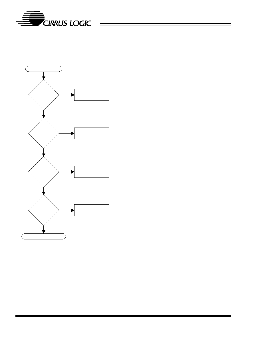
94
DS271PP4
CS8900A
Crystal LANTM ISA Ethernet Controller
CIRRUS LOGIC PRODUCT DATASHEET
Figure 26 shows the steps the CS8900A goes
through in determining when to automatically
switch to DMA.
Whenever the CS8900A automatically enters
DMA, at least one complete frame is already stored
in the on-chip buffer. Because frames are trans-
ferred to the host in the same order as received (first
in, first out), the beginning of the received frame
that triggered the switch to DMA is not the first
frame to be transferred. Instead, the oldest noncom-
mitted frame in the on-chip buffer is the first frame
to use DMA. When DMA begins, any pending Rx-
Event reports in the Interrupt Status Queue are dis-
carded because the host cannot process those
events until the corresponding frames have been
completely DMAed.
Auto-Switch DMA works only on entire received
frames. The CS8900A does not use Auto-Switch
DMA to transfer partial frames. Also, when a frame
has been committed (see Section 5.2.5 on page 83),
the CS8900A will not switch to DMA mode until
the committed frame has been transferred com-
pletely or skipped.
After a complete frame has been moved to host
memory, the CS8900A updates the DMA Start-of-
Frame register (PacketPage base + 0126h), the
DMA Frame Count register (PacketPage base +
0128h), and the DMA Byte Count register, then
sets the RxDMAFrame bit (Register C, BufEvent,
bit 7). If RxDMAiE (Register B, BufCFG, bit 7) is
set, a corresponding interrupt occurs.
5.5.4 DMA Channel Speed vs. Missed Frames
When the CS8900A starts DMA, the entire oldest,
noncommitted frame must be placed in host mem-
ory before on-chip buffer space will be freed for the
next incoming frame. If the oldest frame is relative-
ly large, and the next incoming frame also large,
the incoming frame may be missed, depending on
the speed of the DMA channel. If this happens, the
CS8900A will increment the RxMiss counter (Reg-
ister 10) and clear any event reports (RxEvent and
BufEvent) associated with the missed frame.
5.5.5 Exit From DMA
When the CS8900A has activated receive DMA, it
remains in DMA mode until all of the following are
true:
�
The host processes all RxEvent and BufEvent
reports pending in the ISQ.
All Frames
use DMA
Yes
Yes
No
No
Yes
No
No
Yes
Frame
Discarded
Frame Buffered
in On-chip RAM
Auto-Switch
DMA Disabled
Packet Received
Auto-Switch to DMA
Frame
Passed the
DA filter?
RxDMA only
Bit=1
More
Buffer Space
Available?
AutoRxDMA
Bit=1?
Figure 26. Conditions for Switching to DMA

DS271PP4
95
CS8900A
Crystal LANTM ISA Ethernet Controller
CIRRUS LOGIC PRODUCT DATASHEET
�
The host reads a zero value from the DMA
Frame Count register (PacketPage base +
0028h).
�
The CS8900A is not in the process of transfer-
ring a frame via DMA.
5.5.6 Auto-Switch DMA Example
Figure 27 shows how the CS8900A enters and exits
Auto-Switch DMA mode.
5.6 StreamTransfer
5.6.1 Overview
The CS8900A supports an optional feature,
StreamTransfer, that can reduce the amount of
CPU overhead associated with frame reception.
StreamTransfer works during periods of high re-
ceive activity by grouping multiple receive events
into a single interrupt, thereby reducing the number
of receive interrupts to the host processor. During
periods of peak loading, StreamTransfer will elim-
inate 7 out of every 8 interrupts, cutting interrupt
overhead by up to 87%.
5.6.2 Configuring the CS8900A for
StreamTransfer
StreamTransfer is enabled by setting the StreamE
bit along with either the AutoRxDMAE bit or the
RxDMAonly bit in register Receiver Configuration
(register 3). (StreamTransfer must not be selected
unless either one of AutoRxDMAE or RxDMA-
only is selected.)StreamTransfer only applies to
"good" frames (frames of legal length with valid
CRC). Therefore, the RxOKA bit and the RxOKiE
bit must both be set. Finally, StreamTransfer works
on whole packets and is not compatible with early
interrupts. This requires that the RxDestiE bit and
the Rx128iE bit both be clear.
Table 28 summarizes how to configure the
CS8900A for StreamTransfer.
5.6.3 StreamTransfer Operation
When StreamTransfer is enabled, the CS8900A
will initiate a StreamTransfer cycle whenever two
or more frames with the following characteristics
are received:
1) pass the Destination Address filter;
2) are of legal length with valid CRC; and,
3) are spaced "back-to-back" (between 9.6 and 52
�s apart).
During a StreamTransfer cycle the CS8900A does
the following:
�
delays the normal RxOK interrupt associated
with the first receive frame;
�
switches to receive DMA mode;
�
transfers up to eight receive frames into host
memory via DMA;
�
updates the DMA Start-of-Frame register
(PacketPage base + 0026h);
�
updates the DMA Frame Count register (Pack-
etPage base + 0028h);
�
updates DMA Byte Count register (PacketPage
base + 002Ah);
�
sets the RxDMAFrame bit (Register C, BufE-
vent, Bit 7); and,
�
generates an RxDMAFrame interrupt.
5.6.4 Keeping StreamTransfer Mode Active
When the CS8900A initiates a StreamTransfer cy-
cle, it will continue to execute cycles as long as the
following conditions hold true:
Register Name
Bit
Bit Name
Value
Register 3, RxCFG
7
StreamE
1
8
RxOKiE
1
9
or
A
RxDMAonly
or
AutoRxDMA
1
or
1
Register 5, RxCTL
8
RxOKA
1
Register B, BufCFG
7
RxDMAiE
1
F
RxDestiE
0
B
Rx128iE
0
Table 28. Stream Transfer Configuration
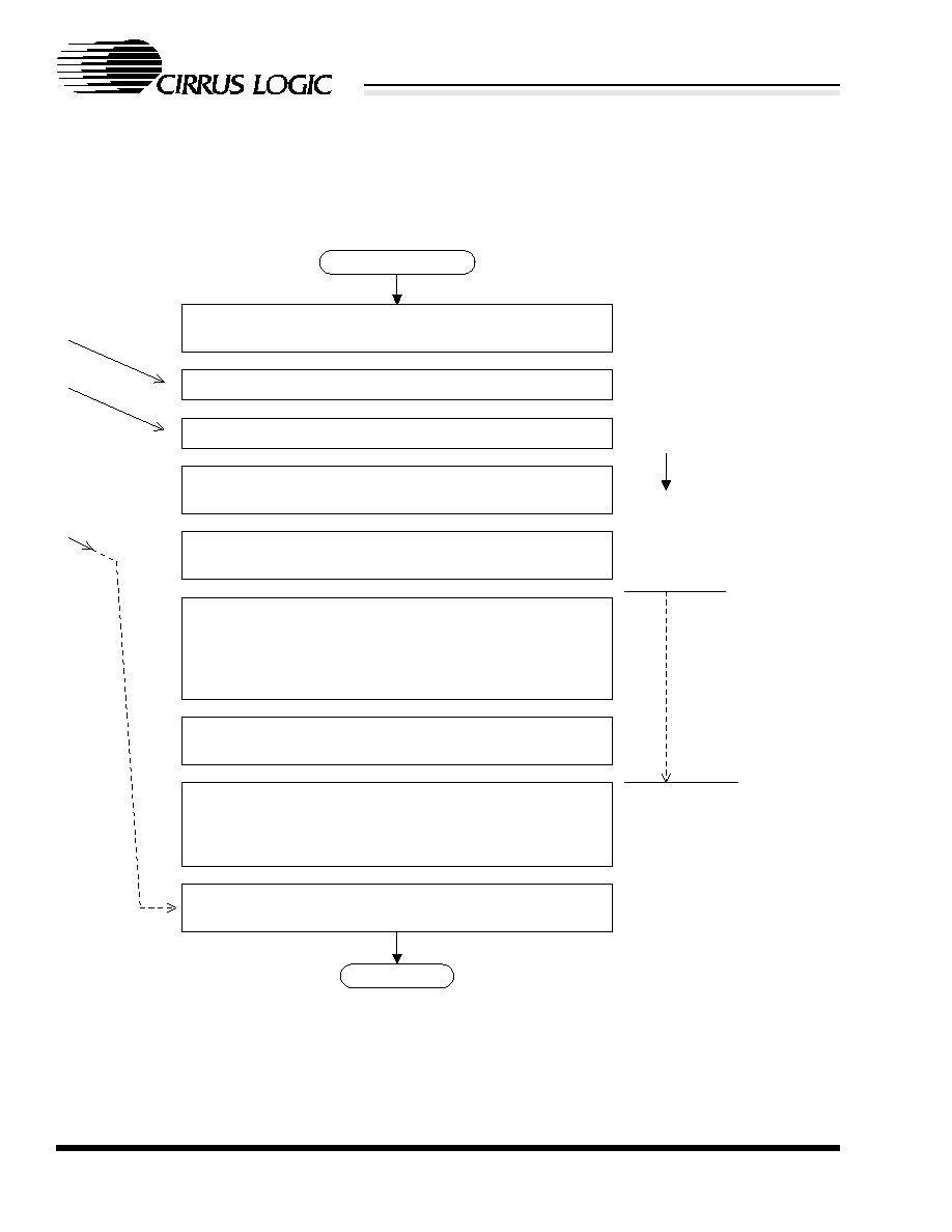
96
DS271PP4
CS8900A
Crystal LANTM ISA Ethernet Controller
CIRRUS LOGIC PRODUCT DATASHEET
Fram
e 1
Fram
e 2
Frame 3 starts to be received and passes the DA filter.
This activates Auto-Switch DMA.
Fram
e 3
Frame 1 is placed in host memory via DMA freeing
space for the incoming Frame 3. The CS8900A updates
the DMA Frame Count, DMA Start of Frame and DMA
Byte Count registers. It then sets the RxDMA DMAFrame
bit and generates an interrupt.
Frame 2 is placed in host memory via DMA and the
CS8900A updates the DMA registers.
The host responds to the RxDMAFrame interrupt, and
reads the Frame Count register, which is cleared when
read. Since there are no receive interrupts pending, the
CS8900A exits DMA (assumes Frame 3 is still coming in).
Receive DMA used
during this time.
At this point, the CS8900A does not have sufficient buffer
space for another complete large frame (1518 bytes).
Frame 1 received and completely stored in on-chip RAM.
Frame 2 received and completely stored in on-chip RAM.
Enter Example Here
Exit Example
Time
Frame 3 is completely buffered in on-chip RAM, and
awaits processing by the host.
Entering this example, the receive buffer is empty and the
DMA Frame Count (PacketPage base + 0028h) is zero.
Figure 27. Example of Auto-Switch DMA

DS271PP4
97
CS8900A
Crystal LANTM ISA Ethernet Controller
CIRRUS LOGIC PRODUCT DATASHEET
�
all packets received are of legal length with val-
id CRC;
�
each packet follows its predecessor by less than
52 ms; and,
�
the DA of each packet passes the DA filter.
If any of these conditions are not met, the CS8900A
exits StreamTransfer by generating RxOK and
RxDMA interrupts. The CS8900A then returns to
either Memory, I/O, or DMA mode, depending on
configuration.
5.6.5 Example of StreamTransfer
Figure 28 shows how four back-to-back frames,
followed by five back-to-back frames, would be re-
ceived without StreamTransfer. Figure 29 shows
how the same sequence of frames would be re-
ceived with StreamTransfer.
5.6.6 Receive DMA Summary
Table 29 summarize the Receive DMA configura-
tion options supported by the CS8900A.
4 Back-to-Back Frames
5 Back-to-Back Frames
Interrupt
Request
9 Interrupts for 9 "Good" Packets
Time
T > 52 us
Figure 28. Receive Example Without Stream Transfer
4 Back-to-Back Frames
5 Back-to-Back Frames
Interrupt
Request
2 Interrupts for 9 "Good" Packets
Time
T > 52 us
Figure 29. Receive DMA Configuration Options
RxDMAonly
(Register 3,
RxCFG,Bit 9)
AutoRxDMAiE
(Register 3,
RxCFG, Bit A)
RxDMAiE
(Register B,
BufCFG, Bit 7)
RxOKiE
(Register 3,
RxCFG, Bit 8)
CS8900A Configuration
1
NA
0
NA
Receive DMA used for all receive frames, without
interrupts.
1
NA
1
NA
Receive DMA used for all receive frames, with
BufEvent interrupts.
0
1
0
0
Auto-Switch DMA used if necessary, without inter-
rupts.
0
1
1
1
Auto-Switch DMA used if necessary, with RxEvent
and BufEvent interrupts possible.
0
0
NA
NA
Memory or I/O Mode only.
Table 29. Receive DMA Configuration Options

98
DS271PP4
CS8900A
Crystal LANTM ISA Ethernet Controller
CIRRUS LOGIC PRODUCT DATASHEET
5.7 Transmit Operation
5.7.1 Overview
Packet transmission occurs in two phases. In the
first phase, the host moves the Ethernet frame into
the CS8900A's buffer memory. The first phase be-
gins with the host issuing a Transmit Command.
This informs the CS8900A that a frame is to be
transmitted and tells the chip when (i.e. after 5,
381, or 1021 bytes have been transferred or after
the full frame has been transferred to the CS8900A)
and how the frame should be sent (i.e. with or with-
out CRC, with or without pad bits, etc.). The host
follows the Transmit Command with the Transmit
Length, indicating how much buffer space is re-
quired. When buffer space is available, the host
writes the Ethernet frame into the CS8900A's inter-
nal memory, using either Memory or I/O space.
In the second phase of transmission, the CS8900A
converts the frame into an Ethernet packet then
transmits it onto the network. The second phase be-
gins with the CS8900A transmitting the preamble
and Start-of-Frame delimiter as soon as the proper
number of bytes has been transferred into its trans-
mit buffer (5, 381, 1021 bytes or full frame, de-
pending on configuration). The preamble and Start-
of-Frame delimiter are followed by the data trans-
ferred into the on-chip buffer by the host (Destina-
tion Address, Source Address, Length field and
LLC data). If the frame is less than 64 bytes, in-
cluding CRC, the CS8900A adds pad bits if config-
ured to do so. Finally, the CS8900A appends the
proper 32-bit CRC value.
5.7.2 Transmit Configuration
After each reset, the CS8900A must be configured
for transmit operation. This can be done automati-
cally using an attached EEPROM, or by writing
configuration commands to the CS8900A's internal
registers (see Section 3.4 on page 20). The items
that must be configured include which physical in-
terface to use and which transmit events cause in-
terrupts.
5.7.2.1 Configuring the Physical Interface
Configuring the physical interface consists of de-
termining which Ethernet interface should be ac-
tive (10BASE-T or AUI), and enabling the transmit
logic for serial transmission. Configuring the Phys-
ical Interface is accomplished via the LineCTL reg-
ister (Register 13) and is described in Table 30.
Note that the CS8900A transmits in 10BASE-T
mode when no link pulses are being received only
if bit DisableLT is set in register Test Control (Reg-
ister 19).
5.7.2.2 Selecting which Events Cause Interrupts
The TxCFG register (Register 7) and the BufCFG
register (Register B) are used to determine which
transmit events will cause interrupts to the host pro-
cessor. Tables 31 and 32 describe the interrupt en-
able (iE) bits in these registers.
5.7.3 Changing the Configuration
When the host configures these registers it does not
need to change them for subsequent packet trans-
missions. If the host does choose to change the Tx-
CFG or BufCFG registers, it may do so at any time.
The effects of the change are noticed immediately.
That is, any changes in the Interrupt Enable (iE)
bits may affect the packet currently being transmit-
ted.
Register 13, LineCTL
Bit
Bit Name
Operation
7
SerTxON
When set, transmission enabled.
8
AUIonly
When set, AUI selected (takes
precedence over AutoAUI/10BT).
When clear, 10BASE-T selected.
9
AutoAUI/10BT When set, automatic interface
selection enabled.
B
Mod
BackoffE
When set, the modified backoff
algorithm is used. When clear,
the standard backoff algorithm is
used.
D
2-part
DefDis
When set, two-part deferral is
disabled.
Table 30. Physical Interface Configuration

DS271PP4
99
CS8900A
Crystal LANTM ISA Ethernet Controller
CIRRUS LOGIC PRODUCT DATASHEET
If the host chooses to change bits in the LineCTL
register after initialization, the ModBackoffE bit
and any receive related bit (LoRxSquelch, SerRx-
ON) may be changed at any time. However, the
Auto AUI/10BT and AUIonly bits should not be
changed while the SerTxON bit is set. If any of
these three bits are to be changed, the host should
first clear the SerTxON bit (Register 13, LineCTL,
Bit 7), and then set it when the changes are com-
plete.
5.7.4 Enabling CRC Generation and Padding
Whenever the host issues a Transmit Request com-
mand, it must indicate whether or not the Cyclic
Redundancy Check (CRC) value should be ap-
pended to the transmit frame, and whether or not
pad bits should be added (if needed). Table 33 de-
scribes how to configure the CS8900A for CRC
generating and padding.
5.7.5 Individual Packet Transmission
Whenever the host has a packet to transmit, it must
issue a Transmit Request to the CS8900A consist-
ing of the following three operations in the exact
order shown:
1) The host must write a Transmit Command to
the TxCMD register (PacketPage base +
0144h). The contents of the TxCMD register
may be read back from the TxCMD register
(Register 9).
2) The host must write the frame's length to the
TxLength register (PacketPage base + 0146h).
3) The host must read the BusST register (Regis-
ter 18)
The information written to the TxCMD register
tells the CS8900A how to transmit the next frame.
Register 7, TxCFG
Bit
Bit Name
Operation
6
Loss-of-
CRSiE
When set, there is an interrupt
whenever the CS8900A fails to
detect Carrier Sense after trans-
mitting the preamble (applies to
the AUI only).
7
SQErroriE
When set, there is an interrupt
whenever there is an SQE error.
8
TxOKiE
When set, there is an interrupt
whenever a frame is transmitted
successfully..
9
Out-of-
windowiE
When set, there is an interrupt
whenever a late collision is
detected.
A
JabberiE
When set, there is an interrupt
whenever there is a jabber condi-
tion.
B
AnycolliE
When set, there is an interrupt
whenever there is a collision.
F
16colliE
When set, there is an interrupt
whenever the CS8900A attempts
to transmit a single frame 16
times.
Table 31. Transmitting Interrupt Configuration
Register B, BufCFG
Bit
Bit Name
Operation
8
Rdy4TxiE
When set, there is an interrupt
whenever buffer space becomes
available for a transmit frame
(used with a Transmit Request).
9
TxUnder
runiE
When set, there is an interrupt
whenever the CS8900A runs out
of data after transmit has started.
C
TxCol
OvfloiE
When set, there is an interrupt
whenever the TxCol counter
overflows.
Table 32. Transmit Interrupt Configuration
Register 9, TxCMD
Inhibit
CRC
(Bit C)
TxPad
Dis
(Bit D)
Operation
0
0
Pad to 64 bytes if necessary
(including CRC).
1
0
Send a runt frame if specified
length less than 60 bytes.
0
1
Pad to 60 bytes if necessary (with-
out CRC).
1
1
Send runt if specified length less
than 64. The CS8900A will not
transmit a frame that is less than 3
bytes.
Table 33. CRC and Paddling Configuration

100
DS271PP4
CS8900A
Crystal LANTM ISA Ethernet Controller
CIRRUS LOGIC PRODUCT DATASHEET
The bits that must be programmed in the TxCMD
register are described in Table 34.
For each individual packet transmission, the host
must issue a complete Transmit Request. Further-
more, the host must write to the TxCMD register
before each packet transmission, even if the con-
tents of the TxCMD register does not change. The
Transmit Request described above may be in either
Memory Space or I/O Space.
5.7.6 Transmit in Poll Mode
In poll mode, Rdy4TxiE bit (Register B, BufCFG,
Bit 8) must be clear (Interrupt Disabled). The trans-
mit operation occurs in the following order and is
shown in Figure 30.
1) The host bids for frame storage by writing the
Transmit Command to the TxCMD register
(memory base+ 0144h in memory mode and
I/O base + 0004h in I/O mode).
2) The host writes the transmit frame length to the
TxLength register (memory base + 0146h in
memory mode and I/O base + 0006h in I/O
mode). If the transmit length is erroneous, the
command is discarded and the TxBidErr bit
(Register 18, BusST, Bit 7) is set.
3) The host reads the BusST register. This read is
performed in memory mode by reading Regis-
ter 18, at memory base + 0138h. In I/O mode,
the host must first set the PacketPage Pointer at
the correct location by writing 0138h to the
PacketPage Pointer Port (I/O base + 000Ah).
The host can then read the BusST register from
the PacketPage Data Port (I/O base + 000Ch).
4) After reading the register, the Rdy4TxNOW bit
(Bit 8) is checked. If the bit is set, the frame can
be written. If the bit is clear, the host must con-
tinue reading the BusST register (Register 18)
and checking the Rdy4TxNOW bit (Bit 8) until
the bit is set.
When the CS8900A is ready to accept the frame,
the host transfers the entire frame from host mem-
ory to CS8900A memory using "REP" instruction
(REP MOVS starting at memory base + 0A00h in
memory mode, and REP OUT to Receive/Transmit
Data Port (I/O base + 0000h) in I/O mode).
5.7.7 Transmit in Interrupt Mode
In interrupt mode, Rdy4TxiE bit (Register B,
BufCFG, Bit 8) must be set for transmit operation.
Transmit operation occurs in the following order
and is shown in Figure 31.
1) The host bids for frame storage by writing the
Transmit Command to the TxCMD register
(memory base + 0144h in memory mode and
I/O base + 0004h in I/O mode).
2) The host writes the transmit frame length to the
TxLength register (memory base + 0146h in
memory mode and I/O base + 0006h in I/O
Register 9, TxCMD
Bit
Bit Name
Operation
6
7
Tx Start
clear clear
Start preamble after 5 bytes
have been transferred to the
CS8900A.
clear
set
Start preamble after 381
bytes have been trans-
ferred to the CS8900A.
set
clear
Start preamble after 1021
bytes have been trans-
ferred to the CS8900A.
set
set
Start preamble after entire
frame has been transferred
to the CS8900A.
8
Force
When set, the CS8900A dis-
cards any frame data cur-
rently in the transmit buffer.
9
Onecoll
When set, the CS8900A will
not attempt to retransmit
any packet after a collision.
C
InhibitCRC When set, the CS8900A
does not append the 32-bit
CRC value to the end of any
transmit packet.
D
TxPadDis
When set, the CS8900A will
not add pad bits to short
frames.
Table 34. Tx Command Configuration
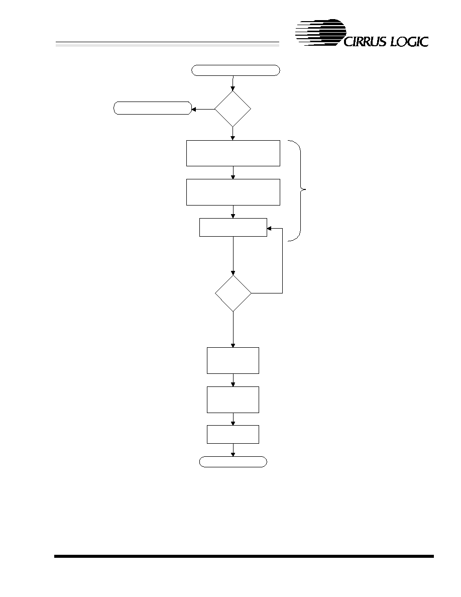
DS271PP4
101
CS8900A
Crystal LANTM ISA Ethernet Controller
CIRRUS LOGIC PRODUCT DATASHEET
mode). If the transmit length is erroneous, the
command is discarded and the TxBidErr, bit 7,
in BusST register is set.
3) The host reads the BusST register. This read is
performed in memory mode by reading Regis-
ter 18, at memory base + 0138h. In I/O mode,
the host must first set the PacketPage Pointer at
CS8900A Commits
Buffer Space to
Transmit Frame
Host Reads the BusST
Register (Register 18)
Transmit Request
Host Writes
Transmit Frame
to CS8900A
Host Writes Transmit Command
to the TxCMD Register
Host Writes Transmit Frame
Length to the TxLength Register
Exit Transmit Process
Yes
No
Enter Packet Transmit Process
Rdy4
TxNOW
bit = 1?
Polling Loop
No
Yes
Is
TxCMD
pending?
Exit: can't Issue command
Note: Issuing a command
at this point will cause
previous transmit frame
to be lost.
CS8900A
Transmits Frame
Figure 30. Transmit Operation in Polling Mode

102
DS271PP4
CS8900A
Crystal LANTM ISA Ethernet Controller
CIRRUS LOGIC PRODUCT DATASHEET
the correct location by writing 0138h to the
PacketPage Pointer Port (I/O base + 000Ah), it
than can read the BusST register from the Pack-
etPage Data Port (I/O base + 000Ch).After
reading the register, the Rdy4TxNOW bit is
checked. If the bit is set, the frame can be writ-
ten to CS8900A memory. If Rdy4TxNOW is
clear, the host will have to wait for the
CS8900A buffer memory to become available
at which time the host will be interrupted. On
interrupt, the host enters the interrupt service
routine and reads ISQ register (Memory base +
0120h in memory mode and I/O base + 0008h
in I/O) and checks the Rdy4Tx bit (bit 8). If
Rdy4Tx is clear then the CS8900A waits for the
next interrupt. If Rdy4Tx is set, then the
CS8900A is ready to accept the frame.
4) When the CS8900A is ready to accept the
frame, the host transfers the entire frame from
host memory to CS8900A memory using REP
instruction (REP MOVS to memory base +
0A00h in memory mode, and REP OUT to Re-
ceive/Transmit Data Port (I/O base + 0000h) in
I/O mode).
5.7.8 Completing Transmission
When the CS8900A successfully completes trans-
mitting a frame, it sets the TxOK bit (Register 8,
TxEvent, Bit 8). If the TxOKiE bit (Register 7, Tx-
CFG, bit 8) is set, the CS8900A generates a corre-
sponding interrupt.
5.7.9 Rdy4TxNOW vs. Rdy4Tx
The Rdy4TxNOW bit (Register 18, BusST, bit 8) is
used to tell the host that the CS8900A is ready to
accept a frame for transmission. This bit is used
during the Transmit Request process or after the
Transmit Request process to signal the host that
space has become available when interrupts are not
being used (i.e. the Rdy4TxiE bit (Register B,
BufCFG, Bit 8) is not set). Also, the Rdy4Tx bit is
used with interrupts and requires the Rdy4TxiE bit
be set.
Figure 30 provides a diagram of error free trans-
mission without collision.
5.7.10 Committing Buffer Space to a Transmit
Frame
When the host issues a transmit request, the
CS8900A checks the length of the transmit frame
to see if there is sufficient on-chip buffer space. If
there is, the CS8900A sets the Rdy4TxNOW bit. If
not, and the Rdy4TxiE bit is set, the CS8900A
waits for buffer space to free up and then sets the
Rdy4Tx bit. If Rdy4TxiE is not set, the CS8900A
sets the Rdy4TxNOW bit when space becomes
available.
Even though transmit buffer space may be avail-
able, the CS8900A does not commit buffer space to
a transmit frame until all of the following are true:
1) The host must issues a Transmit Request;
2) The Transmit Request must be successful; and,
3) Either the host reads that the Rdy4TxNOW bit
(Register 18, BusST, Bit 8) is set, or the host
reads that the Rdy4Tx bit (Register C, BufE-
vent, bit 8) is set.
If the CS8900A commits buffer space to a particu-
lar transmit frame, it will not allow subsequent
frames to be written to that buffer space as long as
the transmit frame is committed.
After buffer space is committed, the frame is sub-
sequently transmitted unless any of the following
occur:
1) The host completely writes the frame data, but
transmission failed on the Ethernet line. There
are three such failures, and these are indicated
by three transmit error bits in the TxEvent reg-
ister (Register 8): 16coll, Jabber, or Out-of-
Window.
Or:
2) The host aborts the transmission by setting the
Force (Register 9, TxCMD, bit 8) bit. In this
case, the committed transmit frame, as well as
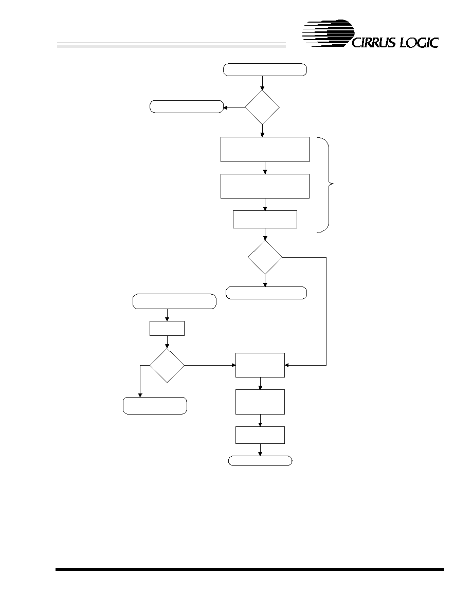
DS271PP4
103
CS8900A
Crystal LANTM ISA Ethernet Controller
CIRRUS LOGIC PRODUCT DATASHEET
any yet-to-be-transmitted frames queued in the
on-chip memory, are cleared and not transmit-
ted. The host should make TxLength = 0 when
using the Force bit.
Or:
3) There is a transmit under-run, and the Tx-
Underrun bit (Register C, BufEvent, Bit 9) is
set.
Successful transmission is indicated when the
TxOK bit (Register 8, TxEvent, Bit 8) is set.
CS8900A Commits
Buffer Space to
Transmit Frame
Host Reads
ISQ
Host Reads the BusST
Register (Register 18)
Transmit Request
Host Writes
Transmit Frame
to CS8900A
Host Writes Transmit Command
to the TxCMD Register
Host Writes Transmit Frame
Length to the TxLength Register
Rdy4Tx
bit = 1?
Exit Transmit Process
No
Yes
No
Yes
Rdy4
TxNOW
bit = 1?
Host Enters Interrupt Routine
Exit WAIT-for-interrupt
Process other events
that caused interrupt
No
Yes
Is
TxCMD
pending?
Exit: can't Issue command
Note: Issuing a command
at this point will cause
previous transmit frame
to be lost.
Enter Packet Transmit Process
CS8900A
Transmits Frame
Figure 31. Transmit Operation in Interrupt Mode

104
DS271PP4
CS8900A
Crystal LANTM ISA Ethernet Controller
CIRRUS LOGIC PRODUCT DATASHEET
5.7.11 Transmit Frame Length
The length of the frame transmitted is determined
by the value written into the TxLength register
(PacketPage base + 0146h) during the Transmit
Request. The length of the transmit frame may be
modified by the configuration of the TxPadDis bit
(Register 9, TxCMD, Bit D) and the InhibitCRC bit
(Register 9, TxCMD, Bit C). Table 35 defines how
these bits affect the length of the transmit frame. In
addition, it shows which frames the CS8900A will
send.
5.8 Full duplex Considerations
The driver should not bid to transmit a long frame
(i.e., a frame greater than 118 bytes) if the prior
transmit frame is still being transmitted. The end of
the transmission of this prior frame is indicated by
a TxOK bit being set in the TxEvent register (reg-
ister 8).
5.9 Auto-Negotiation Considerations
When the CS8900A is connected to an auto negoti-
ation hub, and if auto-media detection is selected
(bits 8 and 9 of register 13), then the CS8900A may
not auto-select the 10BASE-T media. The cause of
this situation is described in the following para-
graphs.
The original IEEE 802.3 specification requires the
MAC to wait until 4 valid link-pulses are received
before asserting Link-OK. Any time an invalid
link-pulse is received, the count is restarted. When
auto-negotiation occurs, a transmitter sends FLPs
(auto-negotiation Fast Link Pulses) bursts instead
of the original IEEE 802.3 NLP (Normal Link
Pulses).
If the hub is attempting to auto-negotiate with the
CS8900A, the CS8900A will never get more than 1
"valid" link pulse (valid NLP). This is not a prob-
lem if the CS8900A is already sending link-pulses,
because when the hub receives NLPs from the
CS8900A, the hub is required to stop sending FLPs
and start sending NLPs. The NLP transmitted by
the hub will put the CS8900A into Link-OK.
However, if the CS8900A is in Auto-Switch mode,
the CS8900A will never send any link-pulses, and
the hub will never change from sending FLPs to
sending NLPs.
Register 9, TxCMD
Host specified transmit length at 0146h (in bytes)
TxPad-
Dis (Bit D)
InhibitCRC
(Bit C)
3 < TxLength < 60
60 < TxLength <
1514
1514 < TxLength < 1518
TxLength > 1518
0
0
Pad to 60 and add
CRC
Send frame and add
CRC [Normal Mode]
Will not send
Will not send
0
1
Pad to 60 and
send without CRC
Send frame without
CRC
Send frame without
CRC
Will not send
1
0
Send without
pads, and add
CRC
Send frame and add
CRC
Will not send
Will not send
1
1
Send without
pads and without
CRC
Send frame without
CRC
Send frame without
CRC
Will not send
Notes: 8. If the TxPadDis bit is clear and InhibitCRC is set and the CS8900A is commanded to send a frame of
length less than 60 bytes, the CS8900A pads.
9. The CS8900A will not send a frame with TxLength less than 3 bytes.
Table 35. Transmit Frame Length

DS271PP4
105
CS8900A
Crystal LANTM ISA Ethernet Controller
CIRRUS LOGIC PRODUCT DATASHEET
6.0 TEST MODES
6.0.1 Loopback & Collision Diagnostic Tests
Internal and external Loopback and Collision tests
can be used to verify the CS8900A's functionality
when configured for either 10BASE-T or AUI op-
eration.
6.0.2 Internal Tests
Internal tests allow the major digital functions to be
tested, independent of the analog functions. During
these tests, the Manchester encoder is connected to
the decoder. All digital circuits are operational, and
the transmitter and receiver are disabled.
6.0.3 External Tests
External test modes allow the complete chip to be
tested without connecting it directly to an Ethernet
network.
6.0.4 Loopback Tests
During Loopback tests, the internal Carrier Sense
(CRS) signal, used to detect collisions, is ignored,
allowing packet reception during packet transmis-
sion.
6.0.5 10BASE-T Loopback and Collision Tests
10BASE-T Loopback and Collision Tests are con-
trolled by two bits in the Test Control register:
FDX (Register 19, TestCTL, Bit E) and ENDE-
Cloop (Register 19, TestCTL, Bit 9). Table 36 de-
scribes these tests.
6.0.6 AUI Loopback and Collision Tests
AUI Loopback and Collision tests are controlled by
two bits in the Test Control register: AUIloop
(Register 19, TestCTL, Bit A) and ENDECloop
(Register 19, TestCTL, Bit 9). Table 37 describes
these tests.
Test Mode
FDX
ENDECloop
Description of Test
10BASE-T Inter-
nal Loopback
1
1
Transmit a frame and verify that the frame is received without
error.
10BASE-T Inter-
nal Collision
0
1
Transmit frames and verify that collisions are detected and
that the internal counters function properly. After 16 collisions,
verify that 16coll (Register 8, TxEvent, Bit F) is set.
10BASE-T
External Loop-
back
1
0
Connect TXD+ to RXD+ and TXD- to RXD-. Transmit a frame
and verify that the frame is received without error.
10BASE-T
External Collision
0
0
Connect TXD+ to RXD+ and TXD- to RXD-. Transmit frames
and verify that collisions are detected and that internal
counters function properly. After 16 collisions, verify that
16coll (Register 8, TxEvent, Bit F) is set.
Table 36. 10BASE-T Loopback and Collision Tests
Test Mode
AUIloop ENDECloop
Description of Test
AUI Internal
Loopback
1
1
Transmit a frame and verify that the frame is received without error.
AUI External
Loopback
1
0
Connect DO+ to DI+ and DO- to DI-. Transmit a frame and verify
that the frame is received without error (since there is no collision
signal, an SQE error will occur).
AUI Collision
0
0
Start transmission and observe DO+/DO- activity. Input a 10 MHz
sine wave to Cl+/Cl- pins and observe collisions.
Table 37. AUI Loopback and Collision Tests
106
DS271PP4
CS8900A
Crystal LANTM ISA Ethernet Controller
CIRRUS LOGIC PRODUCT DATASHEET
6.1 Boundary Scan
Boundary Scan test mode provides an easy and ef-
ficient board-level test for verifying that the
CS8900A has been installed properly. Boundary
Scan will check to see if the orientation of the chip
is correct, and if there are any open or short circuits.
Boundary Scan is controlled by the TEST pin.
When TEST is high, the CS8900A is configured
for normal operation. When TEST is low, the fol-
lowing occurs:
�
the CS8900A enters Boundary Scan test mode
and stays in this mode as long as TEST is low;
�
the CS8900A goes through an internal reset and
remains in internal reset as long as TEST is
low;
�
the AEN pin, normally the ISA bus Address
Enable, is redefined to become the Boundary
Scan shift clock input; and
�
all digital outputs and bi-directional pins are
placed in a high-impedance state (this electri-
cally isolates the CS8900A digital outputs from
the rest of the circuit board).
For Boundary Scan to be enabled, AEN must be
low before TEST is driven low.
A complete Boundary Scan test is made up of two
separate cycles. The first cycle, known as the Out-
put Cycle, tests all digital output pins and all bi-di-
rectional pins. The second cycle, known as the
Input Cycle, tests all digital input pins and all bi-di-
rectional pins.
6.1.1 Output Cycle
During the Output Cycle, the falling edge of AEN
causes each of the 17 digital output pins and each
of the 17 bi-directional pins to be driven low, one
at a time. The cycle begins with LINKLED and ad-
vances in order counterclockwise around the chip
through all 34 pins. This test is referred to as a
"walking 0" test.
The following is a list of output pins and bi-direc-
tional pins that are tested during the Output Cycle:
The output pins not included in this test are:
6.1.2 Input Cycle
During the Input Cycle, the falling edge of AEN
causes the state of each selected pin to be trans-
ferred to EEDataOut (that is, EEDataOut will be
high or low depending on the input level of the se-
lected pin). This cycle begins with SLEEP and ad-
vances clockwise through each of 33 input pins (all
digital input pins except for AEN) and each of the
17 bi-directional pins, one pin at a time.
The following is a list of input pins and bi-direc-
tional pins that are tested during the Input Cycle:
Pin Name
Pin #
Pin Name
Pin #
ELCS
2
INTRQ1
31
EECS
3
INTRQ0
32
EESK
4
IOCS16
33
EEDataOut
5
MEMCS16
34
DMARQ2
11
INTRQ3
35
DMARQ1
13
IOCHRDY
64
DMARQ0
15
SD0 - SD7 65-68, 71-74
CSOUT
17
BSTATUS
78
SD08-SD15 27-24, 21-18
LINKLED
99
INTRQ2
30
LANLED
100
Table 38.
Pin Name
Pin #
Pin Name
Pin #
DO+
83
TXD-
88
DO-
84
RES
93
TXD+
87
XTAL2
98
Table 39.
Pin Name
Pin #
Pin Name
Pin #
ELCS
2
SBHE
36
EEDataIn
6
SA0 - SA11
37-48
CHIPSEL
7
REFRESH
49
DMACK2
12
SA12 - SA19 50-54, 58-60
DMACK1
14
IOR
61
DMACK0
16
IOW
62
SD08-SD15 27-24, 21-18
SD0 - SD7
65-68, 71-74
MEMW
28
RESET
75
MEMR
29
SLEEP
77
Table 40.

DS271PP4
107
CS8900A
Crystal LANTM ISA Ethernet Controller
CIRRUS LOGIC PRODUCT DATASHEET
The input pins not included in this test are:
After the Input Cycle is complete, one more cycle
of AEN returns all digital output pins and bi-direc-
tional pins to a high-impedance state.
6.1.3 Continuity Cycle
The combination of a complete Output Cycle, a
complete Input Cycle, and an additional AEN cycle
is called a Continuity Cycle. Each Continuity Cycle
lasts for 85 AEN clock cycles. The first Continuity
Cycle can be followed by additional Continuity
Cycles by keeping TEST low and continuing to cy-
cle AEN. When TEST is driven high, the CS8900A
exits Boundary Scan mode and AEN is again used
as the ISA-bus Address Enable.
Figure 32 shows a complete Boundary Scan Conti-
nuity Cycle.
Figure 33 shows Boundary Scan timing.
Pin Name
Pin #
Pin Name
Pin #
AEN
63
Cl-
82
TEST
76
RXD+
91
Dl+
79
RXD-
92
Dl-
80
XTAL1
97
Cl+
81
Table 41.
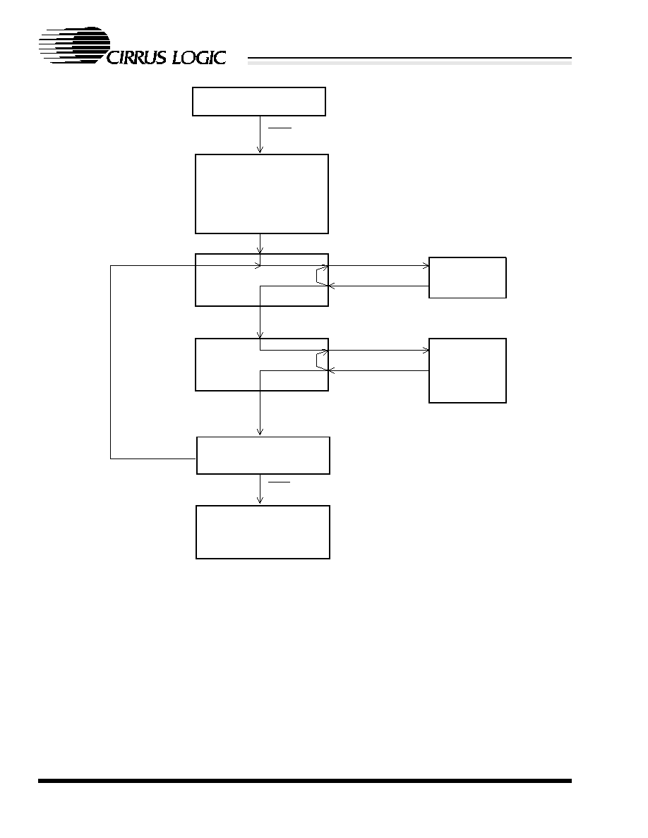
108
DS271PP4
CS8900A
Crystal LANTM ISA Ethernet Controller
CIRRUS LOGIC PRODUCT DATASHEET
ENTER BOUNDARY SCAN:
CS8900A resets, all digital
output pins and bi-directional
pins enter High-Z state,
and AEN becomes shift clock
AEN switches high
OUTPUT CYCLE
AEN switches low
Selected output
goes low
AEN switches high
34 cycles
INPUT CYCLE
AEN switches low
Selected input
copied out
to the
EEDataOut
pin
AEN switches high
50 cycles
All digital output pins and
bi-directional pins enters
High-Z state
TEST switches low (AEN must be low)
Not in Boundary Scan
Test Mode
AEN switches low
AEN switches high
EXIT BOUNDARY SCAN:
AEN becomes ISA bus
Address Enable
TEST switches high
Figure 32. Boundary Scan Continuity Cycle
DS271PP4
109
CS8900A
Crystal LANTM ISA Ethernet Controller
CIRRUS LOGIC PRODUCT DATASHEET
TESTSEL
AEN
Outputs
All outputs
tri-state
LANLED
low
BSTATUS
low
EEDataOut
RESET
copied
out
ELCS
copied
out
OUTPUTS
Hi Z
OUTPUT
TEST
34 Clocks
INPUT
TEST
50 Clocks
OUTPUTS
Hi Z
1 clock
COMPLETE CONTINUITY CYCLE
85 Clocks
LINKLED
low
SLEEP
copied
out
Figure 33. Boundary Scan Timing

110
DS271PP4
CS8900A
Crystal LANTM ISA Ethernet Controller
CIRRUS LOGIC PRODUCT DATASHEET
7.0 CHARACTERISTICS/SPECIFICATIONS - COMMERCIAL
7.1 ABSOLUTE MAXIMUM RATINGS
(AVSS, DVSS = 0 V, all voltages with respect to 0 V.)
WARNING:
Normal operation is not guaranteed at these extremes.
7.2 RECOMMENDED OPERATING CONDITIONS
(AVSS, DVSS = 0 V, all voltages with
respect to 0 V.)
7.3 DC CHARACTERISTICS
(T
A
= 25 �C; VDD = 5.0 V or VDD = 3.3V)
Notes: 1. With digital outputs connected to CMOS loads.
Parameter
Symbol
Min
Max
Unit
Power Supply
Digital
Analog
D
V
DD
A
V
DD
-0.3
-0.3
6.0
6.0
V
V
Input Current
(Except Supply Pins)
-
�10.0
mA
Analog Input Voltage
-0.3
(
A
V
DD
+) + 0.3
V
Digital Input Voltage
-0.3
(
D
V
DD
) + 0.3
V
Ambient Temperature
(Power Applied)
-55
+125
�C
Storage Temperature
-65
+150
�C
Parameter
Symbol
Min
Max
Unit
5.0V Power Supply CS8900A-CQ & -IQ
Digital
Analog
D
V
DD
A
V
DD
4.75
4.75
5.25
5.25
V
V
3.3V Power Supply CS8900A-CQ3 & -IQ3
Digital
Analog
D
V
DD
A
V
DD
3.135
3.135
3.465
3.465
V
V
Operating Ambient Temperature CS8900A-CQ & -CQ3
T
A
0
+70
�C
Operating Ambient Temperature CS8900A-IQ & -IQ3
T
A
-40
+85
�C
Parameter
Symbol
Min
Max
Unit
Crystal (when using external clock - square wave)
XTAL1 Input Low Voltage
V
IXH
-0.5
0.4
V
XTAL1 Input High Voltage
V
IXH
3.5
D
V
DD
+ 0.5
V
XTAL1 Input Low Current
I
IXL
-40
-
�A
XTAL1 Input High Current
I
IXH
-
40
�A
Power Supply
Power Supply Current while Active 5.0V
I
DD
-
55
mA
Power Supply Current while Active 3.3V
I
DD
-
45
mA
Hardware Standby Mode Current
(Note 1) I
DDSTNDBY
-
1.0
mA
Hardware Suspend Mode Current
(Note 1) I
DDHWSUS
-
100
�A
Software Suspend Mode Current
(Note 1) I
DDSWSUS
-
1.0
mA

DS271PP4
111
CS8900A
Crystal LANTM ISA Ethernet Controller
CIRRUS LOGIC PRODUCT DATASHEET
DC CHARACTERISTICS
(Continued)
Notes: 2. OD24: Open Drain Output with 24 mA Drive
OD10: Open Drain Output with 10 mA Drive
B24: Bi-Directional with 3-State Output and 24 mA Drive
B4w: Bi-Directional with 3-State Output, Internal Weak Pullup, and 4 mA Drive
O24ts: 3-State Output with 24 mA Drive
O4: Output with 4 mA Drive
I: Input
Iw: Input with Internal Weak Pullup
Parameter
Symbol
Min
Typ
Max
Unit
Digital Inputs and Outputs
(Note 2)
Output Low Voltage
I
OL
= 24 mA
OD24, B24, O24ts
I
OL
= 10 mA
OD10
I
OL
= 4 mA
B4w, O4
V
OL
-
-
-
-
-
-
0.4
0.4
0.4
V
V
V
Output Low Voltage (all outputs) V
DD
= 3.3V and T
A
= >70�C
V
OL
0.425
V
Output High Voltage
I
OH
= -12 mA
B24
I
OH
= -2 mA
B4w, O24ts, O4
V
OH
2.4
2.4
-
-
-
-
V
V
Output Leakage Current
0
V
OUT
V
CC
OD24, OD10, B24, O24ts
B4w
I
LL
-10
-20
-
-
10
10
�A
Input Low Voltage
I, Iw
V
IL
-
-
0.8
V
Input High Voltage
I, Iw
V
IH
2.4
-
-
V
Input Leakage Current
0
V
IN
V
CC
I
Iw
I
L
-10
-20
-
-
10
10
�A
10BASE-T Interface
Transmitter Differential Output Voltage (Peak)
V
OD
2.2
-
2.8
V
Receiver Normal Squelch Level (Peak)
V
ISQ
300
-
525
mV
Receiver Low Squelch Level (LoRxSquelch bit set)
V
SQL
125
-
290
mV
AUI Interface
Transmitter Differential Output Voltage (DO+/DO- Peak)
V
AOD
�0.45
-
�1.2
V
Transmitter Undershoot Voltage
V
AODU
-
-
100
mV
Transmitter Differential Idle Voltage (DO+/DO- Peak)
V
IDLE
-
-
40
mV
Receiver Squelch Level (DI+/DI- Peak)
V
AISQ
180
-
300
mV

112
DS271PP4
CS8900A
Crystal LANTM ISA Ethernet Controller
CIRRUS LOGIC PRODUCT DATASHEET
7.4 SWITCHING CHARACTERISTICS
(T
A
= 25 �C; V
DD
= 5.0 V or VDD = 3.3V)
Parameter
Symbol
Min
Typ
Max
Unit
16-Bit I/O Read, IOCHRDY Not Used
Address, AEN, SBHE active to IOCS16 low
t
IOR1
-
-
35
ns
Address, AEN, SBHE active to IOR active
t
IOR2
10
-
-
ns
IOR low to SD valid
t
IOR3
-
-
135
ns
Address, AEN, SBHE hold after IOR inactive
t
IOR4
0
-
-
ns
IOR inactive to active
t
IOR5
35
-
-
ns
IOR inactive to SD 3-state
t
IOR6
-
30
-
ns
16-Bit I/O Read, With IOCHRDY
IOR active to IORCHRDY inactive
t
IOR7
-
30
-
ns
IOCHRDY low pulse width
t
IOR8
125
-
175
ns
IOCHRDY active to SD valid
t
IOR9
-
-
0
ns
SA [15:0],
AEN, SBHE
Valid Address
IOCS16
IN
DIRECTION:
IN or OUT of chip
IOR
SD [15:0]
Valid Data
OUT
IN
OUT
t
IOR1
t
IOR2
t
IOR3
t
IOR4
t
IOR5
t
IOR6
Figure 34. 16-Bit I/O Read, IOCHRDY not used
SA [15:0],
AEN, SBHE
Valid Address
IOCS16
IN
DIRECTION:
IN or OUT of chip
IOR
SD [15:0]
Valid Data
OUT
IN
OUT
IOCHRDY
OUT
t
IOR7
t
IOR8
t
IOR9
Figure 35. 16-Bit I/O Read, with IOCHRDY

DS271PP4
113
CS8900A
Crystal LANTM ISA Ethernet Controller
CIRRUS LOGIC PRODUCT DATASHEET
SWITCHING CHARACTERISTICS
(Continued)
Parameter
Symbol
Min
Typ
Max
Unit
16-Bit Memory Read, IOCHRDY Not Used
SA [19:0], SBHE, CHIPSEL, active to MEMCS16 low
t
MEMR1
-
-
30
ns
Address, SBHE, CHIPSEL active to MEMR active
t
MEMR2
10
-
-
ns
MEMR low to SD valid
t
MEMR3
-
-
135
ns
Address, SBHE, CHIPSEL hold after MEMR inactive
t
MEMR4
0
-
-
ns
MEMR inactive to SD 3-state
t
MEMR5
-
30
-
ns
MEMR inactive to active
t
MEMR6
35
-
-
ns
16-Bit Memory Read, With IOCHRDY
MEMR low to IOCHRDY inactive
t
MEMR7
-
35
-
ns
IOCHRDY low pulse width
t
MEMR8
125
-
175
ns
IOCHRDY active to SD valid
t
MEMR9
-
-
0
ns
SA [19:0],
SBHE,
CHIPSEL
Valid Address
MEMCS16
IN
DIRECTION:
IN or OUT of chip
MEMR
SD [15:0]
Valid Data
OUT
IN
OUT
t
MEMR1
t
MEMR2
t
MEMR3
t
MEMR4
t
MEMR5
t
MEMR6
Figure 36. 16-Bit Memory Read, IOCHRDY not used
SA [19:0],
SBHE,
CHIPSEL
Valid Address
MEMCS16
IN
DIRECTION:
IN or OUT of chip
MEMR
SD [15:0]
Valid Data
OUT
IN
OUT
IOCHRDY
OUT
t
MEMR7
t
MEMR8
t
MEMR9
Figure 37. 16-Bit Memory Read, with IOCHRDY
114
DS271PP4
CS8900A
Crystal LANTM ISA Ethernet Controller
CIRRUS LOGIC PRODUCT DATASHEET
SWITCHING CHARACTERISTICS
(Continued)
Parameter
Symbol
Min
Typ
Max
Unit
DMA Read
DMACKx active to IOR active
t
DMAR1
60
-
-
ns
AEN active to IOR active
t
DMAR2
10
-
-
ns
IOR active to Data Valid
t
DMAR3
-
-
135
ns
IOR inactive to SD 3-state
t
DMAR4
-
30
-
ns
IOR n-1 high to DMARQx inactive
t
DMAR5
-
-
20
ns
DMACKx, AEN hold after IOR high
t
DMAR6
20
ns
16-Bit I/O Write
Address, AEN, SBHE valid to IOCS16 low
t
IOW1
-
-
35
ns
Address, AEN, SBHE valid to IOW low
t
IOW2
20
-
-
ns
IOW pulse width
t
IOW3
110
-
-
ns
SD hold after IOW high
t
IOW4
0
-
-
ns
IOW low to SD valid
t
IOW5
-
-
10
ns
IOW inactive to active
t
IOW6
35
-
-
ns
Address hold after IOW high
t
IOW7
0
-
-
ns
DIRECTION:
IN or OUT of chip
SD[15:0]
OUT
IOR
DMARQx
OUT
IN
DMACKx
IN
AEN
IN
t
DMA1
IOR
n
IOR
n-1
t
DMA2
Valid
Data
Valid
Data
Valid
Data
t
DMA3
t
DMA5
t
DMA4
t
DMA6
Figure 38. 16-Bit DMA Read
Figure 39. 16-Bit I/O Write
SA [15:0],
AEN, SBHE
Valid Address
IOCS16
IN
DIRECTION:
IN or OUT of chip
IOW
SD [15:0]
Valid Data In
OUT
IN
IN
t
IOW1
t
IOW2
t
IOW3
t
IOW4
t
IOW5
t
IOW6
t
IOW7
DS271PP4
115
CS8900A
Crystal LANTM ISA Ethernet Controller
CIRRUS LOGIC PRODUCT DATASHEET
SWITCHING CHARACTERISTICS
(Continued)
Parameter
Symbol
Min
Typ
Max
Unit
16-Bit Memory Write
Address, SBHE, CHIPSEL valid to MEMCS16 low
t
MEMW1
-
-
30
ns
Address, SBHE, CHIPSEL valid to MEMW low
t
MEMW2
20
-
-
ns
MEMW pulse width
t
MEMW3
110
-
-
ns
MEMW low to SD valid
t
MEMW4
-
-
40
ns
SD hold after MEMW high
t
MEMW5
0
-
-
ns
Address hold after MEMW inactive
t
MEMW6
0
-
-
ns
MEMW inactive to active
t
MEMW7
35
-
-
ns
10BASE-T Transmit
TXD Pair Jitter into 100
Load
t
TTX1
-
-
8
ns
TXD Pair Return to
50 mV after Last Positive Transition
t
TTX2
-
-
4.5
�s
TXD Pair Positive Hold Time at End of Packet
t
TTX3
250
-
-
ns
SA [19:0],
SBHE,
CHIPSEL
Valid Address
MEMCS16
IN
DIRECTION:
IN or OUT of chip
MEMW
SD [15:0]
Valid Data In
OUT
IN
IN
t
MEMW3
t
MEMW4
t
MEMW5
t
MEMW6
t
MEMW7
t
MEMW2
t
MEMW1
Figure 40. 16-Bit Memory Write
TXD�
tTTX1
tTTX3
tTTX2
Figure 41. 10BASE-T Transmit

116
DS271PP4
CS8900A
Crystal LANTM ISA Ethernet Controller
CIRRUS LOGIC PRODUCT DATASHEET
SWITCHING CHARACTERISTICS
(Continued)
Parameter
Symbol
Min
Typ
Max
Unit
10BASE-T Receive
Allowable Received Jitter at Bit Cell Center
t
TRX1
-
-
�13.5
ns
Allowable Received Jitter at Bit Cell Boundary
t
TRX2
-
-
�13.5
ns
Carrier Sense Assertion Delay
t
TRX3
-
540
-
ns
Invalid Preamble Bits after Assertion of Carrier Sense
t
TRX4
1
-
2
bits
Carrier Sense Deassertion Delay
t
TRX5
-
270
-
ns
10BASE-T Link Integrity
First Transmitted Link Pulse after Last Transmitted Packet
t
LN1
8
16
24
ms
Time Between Transmitted Link Pulses
t
LN2
8
16
24
ms
Width of Transmitted Link Pulses
t
LN3
60
100
200
ns
Minimum Received Link Pulse Separation
t
LN4
2
-
7
ms
Maximum Received Link Pulse Separation
t
LN5
25
-
150
ms
Last Receive Activity to Link Fail (Link Loss Timer)
t
LN6
50
-
150
ms
tTRX3
RXD�
tTRX5
tTRX4
tTRX1
tTRX2
Carrier Sense (internal)
Figure 42. 10BASE-T Receive
RXD�
LINKLED
TXD�
t
LN1
t
LN2
t
LN3
t
LN4
t
LN5
tLN6
Figure 43. 10BASE-T Link Integrity
DS271PP4
117
CS8900A
Crystal LANTM ISA Ethernet Controller
CIRRUS LOGIC PRODUCT DATASHEET
SWITCHING CHARACTERISTICS
(Continued)
Parameter
Symbol
Min
Typ
Max
Unit
AUI Transmit
DO Pair Rise and Fall Times
t
ATX1
-
-
5
ns
DO Pair Jitter at Bit Cell Center
t
ATX2
-
-
0.5
ns
DO Pair Positive Hold Time at Start of Idle
t
ATX3
200
-
-
ns
DO Pair Return to
40 mVp after Last Positive Transition
t
ATX4
-
-
8.0
�s
AUI Receive
DI Pair Rise and Fall Time
t
ARX1
-
-
10
ns
Allowable Bit Cell Center and Boundary Jitter in Data
t
ARX2
-
-
�18
ns
Carrier Sense Assertion Delay
t
ARX3
-
240
-
ns
Invalid Preamble Bits after Carrier Sense Asserts
t
ARX4
1
-
2
bits
Carrier Sense Deassertion Delay
t
ARX5
150
-
250
ns
AUI Collision
CI Pair Cycle Time
t
ACL1
85
100
115
ns
CI Pair Rise and Fall Times
t
ACL2
-
-
10
ns
CI Pair Return to Zero from Last Positive Transition
t
ACL3
160
-
-
ns
Collision Assertion Delay
t
ACL4
50
-
200
ns
Collision Deassertion Delay
t
ACL5
150
-
300
ns
DO�
tATX1
tATX1
tATX2
tATX4
tATX3
1
0
0
0
Figure 44. AUI Transmit
DI�
tARX1
tARX2
1
0
1
0
tARX3
tARX4
tARX5
tARX1
Carrier Sense (Internal)
Figure 45. AUI Receive
t
ACL1
CI�
t
ACL4
t
ACL5
Collision (Internal)
t
ACL2
t
ACL2
t
ACL3
Figure 46. AUI Collision

118
DS271PP4
CS8900A
Crystal LANTM ISA Ethernet Controller
CIRRUS LOGIC PRODUCT DATASHEET
SWITCHING CHARACTERISTICS
(Continued)
Parameter
Symbol
Min
Typ
Max
Unit
External Boot PROM Access
Address active to MEMR
t
BPROM1
20
-
-
ns
MEMR active to CSOUT low
t
BPROM2
-
-
35
ns
MEMR inactive to CSOUT high
t
BPROM3
-
-
40
ns
EEPROM
EESK Setup time relative to EECS
t
SKS
100
-
-
ns
EECS/ELCS_b Setup time wrt
EESK
t
CCS
250
-
-
ns
EEDataOut Setup time wrt
EESK
t
DIS
250
-
-
ns
EEDataOut Hold time wrt
EESK
t
DIH
500
-
-
ns
EEDataIn Hold time wrt
EESK
t
DH
10
-
-
ns
EECS Hold time wrt
EESK
t
CSH
100
-
-
ns
Min EECS Low time during programming
t
CS
1000
-
-
ns
SA [19:0]
MEMR
t BPROM1
CSOUT
CS
t BPROM3
t BPROM2
Figure 47. External Boot PROM Access
tCSH
tCS
tSKS
tCSS
tDIS
tDIH
tDH
EESK
EECS
EEData Out
EEData In
(Read)
Figure 48. EEPROM

DS271PP4
119
CS8900A
Crystal LANTM ISA Ethernet Controller
CIRRUS LOGIC PRODUCT DATASHEET
7.5 10BASE-T WIRING
�
If a center tap transformer is used on the RXD+ and RXD- inputs, replace the pair of Rr resistors with
a single 2xRr resistor.
�
The Rt and Rr resistors are �1% tolerance.
�
The CS8900A supports 100, 120, and 150
unshielded twisted pair cables. The proper values of Rt
and Rr, for a given cable impedance, are shown below:
�
Note: for 3.3V operation the turns ratio on TXD+ and TXD- is 1:2.5, rt is 8
for 100
cable and the
68pF cap changes to 560pF.
Cable Impedance (
)
Rt (
)
Rr (
)
100
24.3 49.9
120
30.1 60.4
150
37.4
75
Rt
Rt
CS8900A
TD +
TD -
TXD +
TXD -
1 : 2
RJ45
1
2
1 : 1
RD +
RD -
3
6
0.01
�F
+
RXD+
RXD-
Rr
Rr
0.01
�F
-
68 pF
120
DS271PP4
CS8900A
Crystal LANTM ISA Ethernet Controller
CIRRUS LOGIC PRODUCT DATASHEET
7.6 AUI WIRING
7.7 QUARTZ CRYSTAL REQUIREMENTS
(If a 20 MHz quartz crystal is used, it must meet the
following specifications)
Parameter
Min
Typ
Max
Unit
Parallel Resonant Frequency
-
20
-
MHz
Resonant Frequency Error (C
L
= 18 pF)
-50
-
+50
ppm
Resonant Frequency Change Over Operating Temperature
-40
-
+40
ppm
Crystal Capacitance
-
-
18
pF
Motional Crystal Capacitance
-
0.022
-
pF
Series Resistance
-
-
50
Ohm
Shunt Capacitance
-
-
7
pF
CS8900A
DO +
DO -
1 : 1
DB15
3
10
Tx
4
1 : 1
5
12
13
6
+12 V
+
CI +
CI -
1 : 1
2
9
39.2
39.2
Col
0.01 uF
-
+
DI +
DI -
39.2
39.2
Rx
0.01 uF
-
DS271PP4
121
CS8900A
Crystal LANTM ISA Ethernet Controller
CIRRUS LOGIC PRODUCT DATASHEET
8.0 CHARACTERISTICS/SPECIFICATIONS - INDUSTRIAL
8.1 ABSOLUTE MAXIMUM RATINGS
(AVSS, DVSS = 0 V, all voltages with respect to 0 V.)
WARNING:
Normal operation is not guaranteed at these extremes.
8.2 RECOMMENDED OPERATING CONDITIONS
(AVSS, DVSS = 0 V, all voltages with
respect to 0 V.)
8.3 DC CHARACTERISTICS
(T
A
= 25 �C; VDD = 5.0 V or VDD = 3.3V)
Notes: 1. With digital outputs connected to CMOS loads.
Parameter
Symbol
Min
Max
Unit
Power Supply
Digital
Analog
D
V
DD
A
V
DD
-0.3
-0.3
6.0
6.0
V
V
Input Current
(Except Supply Pins)
-
�10.0
mA
Analog Input Voltage
-0.3
(
A
V
DD
+) + 0.3
V
Digital Input Voltage
-0.3
(
D
V
DD
) + 0.3
V
Ambient Temperature
(Power Applied)
-55
+125
�C
Storage Temperature
-65
+150
�C
Parameter
Symbol
Min
Max
Unit
5.0V Power Supply CS8900A-CQ & -IQ
Digital
Analog
D
V
DD
A
V
DD
4.75
4.75
5.25
5.25
V
V
3.3V Power Supply CS8900A-CQ3 & -IQ3
Digital
Analog
D
V
DD
A
V
DD
3.135
3.135
3.465
3.465
V
V
Operating Ambient Temperature CS8900A-CQ & -CQ3
T
A
0
+70
�C
Operating Ambient Temperature CS8900A-IQ & -IQ3
T
A
-40
+85
�C
Parameter
Symbol
Min
Max
Unit
Crystal (when using external clock - square wave)
XTAL1 Input Low Voltage
V
IXH
-0.5
0.4
V
XTAL1 Input High Voltage
V
IXH
3.5
D
V
DD
+ 0.5
V
XTAL1 Input Low Current
I
IXL
-40
-
�A
XTAL1 Input High Current
I
IXH
-
40
�A
Power Supply
Power Supply Current while Active 5.0V
I
DD
-
55
mA
Power Supply Current while Active 3.3V
I
DD
-
45
mA
Hardware Standby Mode Current
(Note 1) I
DDSTNDBY
-
1.0
mA
Hardware Suspend Mode Current
(Note 1) I
DDHWSUS
-
100
�A
Software Suspend Mode Current
(Note 1) I
DDSWSUS
-
1.0
mA

122
DS271PP4
CS8900A
Crystal LANTM ISA Ethernet Controller
CIRRUS LOGIC PRODUCT DATASHEET
DC CHARACTERISTICS
(Continued)
Notes: 2. OD24: Open Drain Output with 24 mA Drive
OD10: Open Drain Output with 10 mA Drive
B24: Bi-Directional with 3-State Output and 24 mA Drive
B4w: Bi-Directional with 3-State Output, Internal Weak Pullup, and 4 mA Drive
O24ts: 3-State Output with 24 mA Drive
O4: Output with 4 mA Drive
I: Input
Iw: Input with Internal Weak Pullup
Parameter
Symbol
Min
Typ
Max
Unit
Digital Inputs and Outputs
(Note 2)
Output Low Voltage
I
OL
= 24 mA
OD24, B24, O24ts
I
OL
= 10 mA
OD10
I
OL
= 4 mA
B4w, O4
V
OL
-
-
-
-
-
-
0.4
0.4
0.4
V
V
V
Output Low Voltage (all outputs) V
DD
= 3.3V and T
A
= >70�C
V
OL
0.425
V
Output High Voltage
I
OH
= -12 mA
B24
I
OH
= -2 mA
B4w, O24ts, O4
V
OH
2.4
2.4
-
-
-
-
V
V
Output Leakage Current
0
V
OUT
V
CC
OD24, OD10, B24, O24ts
B4w
I
LL
-10
-20
-
-
10
10
�A
Input Low Voltage
I, Iw
V
IL
-
-
0.8
V
Input High Voltage
I, Iw
V
IH
2.4
-
-
V
Input Leakage Current
0
V
IN
V
CC
I
Iw
I
L
-10
-20
-
-
10
10
�A
10BASE-T Interface
Transmitter Differential Output Voltage (Peak)
V
OD
2.2
-
2.8
V
Receiver Normal Squelch Level (Peak)
V
ISQ
300
-
525
mV
Receiver Low Squelch Level (LoRxSquelch bit set)
V
SQL
125
-
290
mV
AUI Interface
Transmitter Differential Output Voltage (DO+/DO- Peak)
V
AOD
�0.45
-
�1.2
V
Transmitter Undershoot Voltage
V
AODU
-
-
100
mV
Transmitter Differential Idle Voltage (DO+/DO- Peak)
V
IDLE
-
-
40
mV
Receiver Squelch Level (DI+/DI- Peak)
V
AISQ
180
-
300
mV

DS271PP4
123
CS8900A
Crystal LANTM ISA Ethernet Controller
CIRRUS LOGIC PRODUCT DATASHEET
8.4 SWITCHING CHARACTERISTICS
(T
A
= 25 �C; V
DD
= 5.0 V or VDD = 3.3V)
Parameter
Symbol
Min
Typ
Max
Unit
16-Bit I/O Read, IOCHRDY Not Used
Address, AEN, SBHE active to IOCS16 low
t
IOR1
-
-
35
ns
Address, AEN, SBHE active to IOR active
t
IOR2
10
-
-
ns
IOR low to SD valid
t
IOR3
-
-
135
ns
Address, AEN, SBHE hold after IOR inactive
t
IOR4
0
-
-
ns
IOR inactive to active
t
IOR5
35
-
-
ns
IOR inactive to SD 3-state
t
IOR6
-
30
-
ns
16-Bit I/O Read, With IOCHRDY
IOR active to IORCHRDY inactive
t
IOR7
-
30
-
ns
IOCHRDY low pulse width
t
IOR8
125
-
175
ns
IOCHRDY active to SD valid
t
IOR9
-
-
0
ns
SA [15:0],
AEN, SBHE
Valid Address
IOCS16
IN
DIRECTION:
IN or OUT of chip
IOR
SD [15:0]
Valid Data
OUT
IN
OUT
t
IOR1
t
IOR2
t
IOR3
t
IOR4
t
IOR5
t
IOR6
Figure 49. 16-Bit I/O Read, IOCHRDY not used
SA [15:0],
AEN, SBHE
Valid Address
IOCS16
IN
DIRECTION:
IN or OUT of chip
IOR
SD [15:0]
Valid Data
OUT
IN
OUT
IOCHRDY
OUT
t
IOR7
t
IOR8
t
IOR9
Figure 50. 16-Bit I/O Read, with IOCHRDY

124
DS271PP4
CS8900A
Crystal LANTM ISA Ethernet Controller
CIRRUS LOGIC PRODUCT DATASHEET
SWITCHING CHARACTERISTICS
(Continued)
Parameter
Symbol
Min
Typ
Max
Unit
16-Bit Memory Read, IOCHRDY Not Used
SA [19:0], SBHE, CHIPSEL, active to MEMCS16 low
t
MEMR1
-
-
30
ns
Address, SBHE, CHIPSEL active to MEMR active
t
MEMR2
10
-
-
ns
MEMR low to SD valid
t
MEMR3
-
-
135
ns
Address, SBHE, CHIPSEL hold after MEMR inactive
t
MEMR4
0
-
-
ns
MEMR inactive to SD 3-state
t
MEMR5
-
30
-
ns
MEMR inactive to active
t
MEMR6
35
-
-
ns
16-Bit Memory Read, With IOCHRDY
MEMR low to IOCHRDY inactive
t
MEMR7
-
35
-
ns
IOCHRDY low pulse width
t
MEMR8
125
-
175
ns
IOCHRDY active to SD valid
t
MEMR9
-
-
0
ns
SA [19:0],
SBHE,
CHIPSEL
Valid Address
MEMCS16
IN
DIRECTION:
IN or OUT of chip
MEMR
SD [15:0]
Valid Data
OUT
IN
OUT
t
MEMR1
t
MEMR2
t
MEMR3
t
MEMR4
t
MEMR5
t
MEMR6
Figure 51. 16-Bit Memory Read, IOCHRDY not used
SA [19:0],
SBHE,
CHIPSEL
Valid Address
MEMCS16
IN
DIRECTION:
IN or OUT of chip
MEMR
SD [15:0]
Valid Data
OUT
IN
OUT
IOCHRDY
OUT
t
MEMR7
t
MEMR8
t
MEMR9
Figure 52. 16-Bit Memory Read, with IOCHRDY
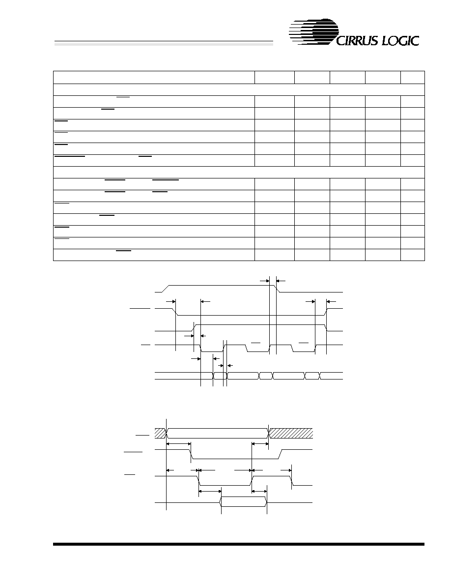
DS271PP4
125
CS8900A
Crystal LANTM ISA Ethernet Controller
CIRRUS LOGIC PRODUCT DATASHEET
SWITCHING CHARACTERISTICS
(Continued)
Parameter
Symbol
Min
Typ
Max
Unit
DMA Read
DMACKx active to IOR active
t
DMAR1
60
-
-
ns
AEN active to IOR active
t
DMAR2
10
-
-
ns
IOR active to Data Valid
t
DMAR3
-
-
135
ns
IOR inactive to SD 3-state
t
DMAR4
-
30
-
ns
IOR n-1 high to DMARQx inactive
t
DMAR5
-
-
20
ns
DMACKx, AEN hold after IOR high
t
DMAR6
20
ns
16-Bit I/O Write
Address, AEN, SBHE valid to IOCS16 low
t
IOW1
-
-
35
ns
Address, AEN, SBHE valid to IOW low
t
IOW2
20
-
-
ns
IOW pulse width
t
IOW3
110
-
-
ns
SD hold after IOW high
t
IOW4
0
-
-
ns
IOW low to SD valid
t
IOW5
-
-
10
ns
IOW inactive to active
t
IOW6
35
-
-
ns
Address hold after IOW high
t
IOW7
0
-
-
ns
DIRECTION:
IN or OUT of chip
SD[15:0]
OUT
IOR
DMARQx
OUT
IN
DMACKx
IN
AEN
IN
t
DMA1
IOR
n
IOR
n-1
t
DMA2
Valid
Data
Valid
Data
Valid
Data
t
DMA3
t
DMA5
t
DMA4
t
DMA6
Figure 53. 16-Bit DMA Read
Figure 54. 16-Bit I/O Write
SA [15:0],
AEN, SBHE
Valid Address
IOCS16
IN
DIRECTION:
IN or OUT of chip
IOW
SD [15:0]
Valid Data In
OUT
IN
IN
t
IOW1
t
IOW2
t
IOW3
t
IOW4
t
IOW5
t
IOW6
t
IOW7

126
DS271PP4
CS8900A
Crystal LANTM ISA Ethernet Controller
CIRRUS LOGIC PRODUCT DATASHEET
SWITCHING CHARACTERISTICS
(Continued)
Parameter
Symbol
Min
Typ
Max
Unit
16-Bit Memory Write
Address, SBHE, CHIPSEL valid to MEMCS16 low
t
MEMW1
-
-
30
ns
Address, SBHE, CHIPSEL valid to MEMW low
t
MEMW2
20
-
-
ns
MEMW pulse width
t
MEMW3
110
-
-
ns
MEMW low to SD valid
t
MEMW4
-
-
40
ns
SD hold after MEMW high
t
MEMW5
0
-
-
ns
Address hold after MEMW inactive
t
MEMW6
0
-
-
ns
MEMW inactive to active
t
MEMW7
35
-
-
ns
10BASE-T Transmit
TXD Pair Jitter into 100
Load
t
TTX1
-
-
8
ns
TXD Pair Return to
50 mV after Last Positive Transition
t
TTX2
-
-
4.5
�s
TXD Pair Positive Hold Time at End of Packet
t
TTX3
250
-
-
ns
SA [19:0],
SBHE,
CHIPSEL
Valid Address
MEMCS16
IN
DIRECTION:
IN or OUT of chip
MEMW
SD [15:0]
Valid Data In
OUT
IN
IN
t
MEMW3
t
MEMW4
t
MEMW5
t
MEMW6
t
MEMW7
t
MEMW2
t
MEMW1
Figure 55. 16-Bit Memory Write
TXD�
tTTX1
tTTX3
tTTX2
Figure 56. 10BASE-T Transmit

DS271PP4
127
CS8900A
Crystal LANTM ISA Ethernet Controller
CIRRUS LOGIC PRODUCT DATASHEET
SWITCHING CHARACTERISTICS
(Continued)
Parameter
Symbol
Min
Typ
Max
Unit
10BASE-T Receive
Allowable Received Jitter at Bit Cell Center
t
TRX1
-
-
�13.5
ns
Allowable Received Jitter at Bit Cell Boundary
t
TRX2
-
-
�13.5
ns
Carrier Sense Assertion Delay
t
TRX3
-
540
-
ns
Invalid Preamble Bits after Assertion of Carrier Sense
t
TRX4
1
-
2
bits
Carrier Sense Deassertion Delay
t
TRX5
-
270
-
ns
10BASE-T Link Integrity
First Transmitted Link Pulse after Last Transmitted Packet
t
LN1
8
16
24
ms
Time Between Transmitted Link Pulses
t
LN2
8
16
24
ms
Width of Transmitted Link Pulses
t
LN3
60
100
200
ns
Minimum Received Link Pulse Separation
t
LN4
2
-
7
ms
Maximum Received Link Pulse Separation
t
LN5
25
-
150
ms
Last Receive Activity to Link Fail (Link Loss Timer)
t
LN6
50
-
150
ms
tTRX3
RXD�
tTRX5
tTRX4
tTRX1
tTRX2
Carrier Sense (internal)
Figure 57. 10BASE-T Receive
RXD�
LINKLED
TXD�
t
LN1
t
LN2
t
LN3
t
LN4
t
LN5
tLN6
Figure 58. 10BASE-T Link Integrity

128
DS271PP4
CS8900A
Crystal LANTM ISA Ethernet Controller
CIRRUS LOGIC PRODUCT DATASHEET
SWITCHING CHARACTERISTICS
(Continued)
Parameter
Symbol
Min
Typ
Max
Unit
AUI Transmit
DO Pair Rise and Fall Times
t
ATX1
-
-
5
ns
DO Pair Jitter at Bit Cell Center
t
ATX2
-
-
0.5
ns
DO Pair Positive Hold Time at Start of Idle
t
ATX3
200
-
-
ns
DO Pair Return to
40 mVp after Last Positive Transition
t
ATX4
-
-
8.0
�s
AUI Receive
DI Pair Rise and Fall Time
t
ARX1
-
-
10
ns
Allowable Bit Cell Center and Boundary Jitter in Data
t
ARX2
-
-
�18
ns
Carrier Sense Assertion Delay
t
ARX3
-
240
-
ns
Invalid Preamble Bits after Carrier Sense Asserts
t
ARX4
1
-
2
bits
Carrier Sense Deassertion Delay
t
ARX5
150
-
250
ns
AUI Collision
CI Pair Cycle Time
t
ACL1
85
100
115
ns
CI Pair Rise and Fall Times
t
ACL2
-
-
10
ns
CI Pair Return to Zero from Last Positive Transition
t
ACL3
160
-
-
ns
Collision Assertion Delay
t
ACL4
50
-
200
ns
Collision Deassertion Delay
t
ACL5
150
-
300
ns
DO�
tATX1
tATX1
tATX2
tATX4
tATX3
1
0
0
0
Figure 59. AUI Transmit
DI�
tARX1
tARX2
1
0
1
0
tARX3
tARX4
tARX5
tARX1
Carrier Sense (Internal)
Figure 60. AUI Receive
t
ACL1
CI�
t
ACL4
t
ACL5
Collision (Internal)
t
ACL2
t
ACL2
t
ACL3
Figure 61. AUI Collision

DS271PP4
129
CS8900A
Crystal LANTM ISA Ethernet Controller
CIRRUS LOGIC PRODUCT DATASHEET
SWITCHING CHARACTERISTICS
(Continued)
Parameter
Symbol
Min
Typ
Max
Unit
External Boot PROM Access
Address active to MEMR
t
BPROM1
20
-
-
ns
MEMR active to CSOUT low
t
BPROM2
-
-
35
ns
MEMR inactive to CSOUT high
t
BPROM3
-
-
40
ns
EEPROM
EESK Setup time relative to EECS
t
SKS
100
-
-
ns
EECS/ELCS_b Setup time wrt
EESK
t
CCS
250
-
-
ns
EEDataOut Setup time wrt
EESK
t
DIS
250
-
-
ns
EEDataOut Hold time wrt
EESK
t
DIH
500
-
-
ns
EEDataIn Hold time wrt
EESK
t
DH
10
-
-
ns
EECS Hold time wrt
EESK
t
CSH
100
-
-
ns
Min EECS Low time during programming
t
CS
1000
-
-
ns
SA [19:0]
MEMR
t BPROM1
CSOUT
CS
t BPROM3
t BPROM2
Figure 62. External Boot PROM Access
tCSH
tCS
tSKS
tCSS
tDIS
tDIH
tDH
EESK
EECS
EEData Out
EEData In
(Read)
Figure 63. EEPROM

130
DS271PP4
CS8900A
Crystal LANTM ISA Ethernet Controller
CIRRUS LOGIC PRODUCT DATASHEET
8.5 10BASE-T WIRING
�
If a center tap transformer is used on the RXD+ and RXD- inputs, replace the pair of Rr resistors with
a single 2xRr resistor.
�
The Rt and Rr resistors are �1% tolerance.
�
The CS8900A supports 100, 120, and 150
unshielded twisted pair cables. The proper values of Rt
and Rr, for a given cable impedance, are shown below:
�
Note: for 3.3V operation the turns ratio on TXD+ and TXD- is 1:2.5, rt is 8
for 100
cable and the
68pF cap changes to 560pF.
Cable Impedance (
)
Rt (
)
Rr (
)
100
24.3 49.9
120
30.1 60.4
150
37.4
75
Rt
Rt
CS8900A
TD +
TD -
TXD +
TXD -
1 : 2
RJ45
1
2
1 : 1
RD +
RD -
3
6
0.01
�F
+
RXD+
RXD-
Rr
Rr
0.01
�F
-
68 pF
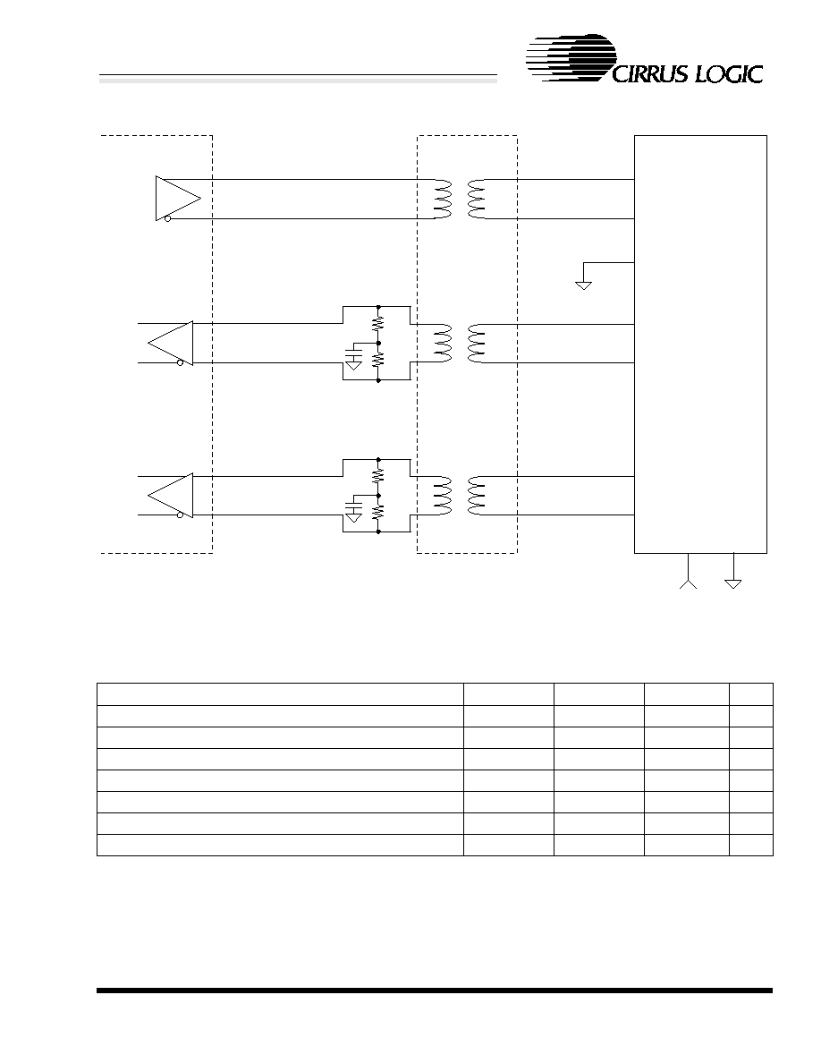
DS271PP4
131
CS8900A
Crystal LANTM ISA Ethernet Controller
CIRRUS LOGIC PRODUCT DATASHEET
8.6 AUI WIRING
8.7 QUARTZ CRYSTAL REQUIREMENTS
(If a 20 MHz quartz crystal is used, it must meet the
following specifications)
Parameter
Min
Typ
Max
Unit
Parallel Resonant Frequency
-
20
-
MHz
Resonant Frequency Error (C
L
= 18 pF)
-50
-
+50
ppm
Resonant Frequency Change Over Operating Temperature
-40
-
+40
ppm
Crystal Capacitance
-
-
18
pF
Motional Crystal Capacitance
-
0.022
-
pF
Series Resistance
-
-
50
Ohm
Shunt Capacitance
-
-
7
pF
CS8900A
DO +
DO -
1 : 1
DB15
3
10
Tx
4
1 : 1
5
12
13
6
+12 V
+
CI +
CI -
1 : 1
2
9
39.2
39.2
Col
0.01 uF
-
+
DI +
DI -
39.2
39.2
Rx
0.01 uF
-
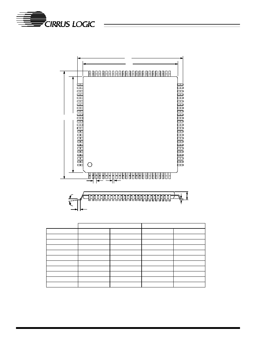
132
DS271PP4
CS8900A
Crystal LANTM ISA Ethernet Controller
CIRRUS LOGIC PRODUCT DATASHEET
9.0 PHYSICAL DIMENSIONS
INCHES
MILLIMETERS
DIM
MIN
MAX
MIN
MAX
A
---
0.063
---
1.60
A1
0.002
0.006
0.05
0.15
B
0.007
0.011
0.17
0.27
D
0.618
0.642
15.70
16.30
D1
0.547
0.555
13.90
14.10
E
0.618
0.642
15.70
16.30
E1
0.547
0.555
13.90
14.10
e*
0.016
0.024
0.40
0.60
L
0.018
0.030
0.45
0.75
0.000�
7.000�
0.00�
7.00�
* Nominal pin pitch is 0.50 mm
Controlling dimension is mm.
JEDEC Designation: MS026
100L TQFP PACKAGE DRAWING
E1
E
D1
D
1
e
L
B
A1
A

DS271PP4
133
CS8900A
Crystal LANTM ISA Ethernet Controller
CIRRUS LOGIC PRODUCT DATASHEET
10.0 GLOSSARY OF TERMS
10.1 Acronyms
AUI
Attachment Unit Interface
CRC
Cyclic Redundancy Check
CS
Carrier Sense
CSMA/CD
Carrier Sense Multiple Access with Collision Detection
DA
Destination Address
EEPROM
Electrically Erasable Programmable Read Only Memory
EOF
End-of-Frame
FCS
Frame Check Sequence
FDX
Full Duplex
IA
Individual Address
IPG
Inter-Packet Gap
ISA
Industry Standard Architecture
LA
ISA Latchable Address Bus (LA17 - LA23)
LLC
Logical Link Control
MAC
Media Access Control
MAU
Medium Attachment Unit
MIB
Management Information Base
RX
Receive
SA
Source Address or ISA System Address Bus (SA0 - SA19)
SFD
Start-of-Frame Delimiter
SNMP
Simple Network Management Protocol
SOF
Start-of-Frame
SQE
Signal Quality Error
TDR
Time Domain Reflectometer
TX
Transmit
UTP
Unshielded Twisted Pair

134
DS271PP4
CS8900A
Crystal LANTM ISA Ethernet Controller
CIRRUS LOGIC PRODUCT DATASHEET
10.2 Definitions
Cyclic Redundancy Check
The method used to compute the 32-bit frame check sequence (FCS).
Frame Check Sequence
The 32-bit field at the end of a frame that contains the result of the cyclic redundancy check
(CRC).
Frame
An Ethernet string of data bits that includes the Destination Address (DA), Source Address
(SA), optional length field, Logical Link Control data (LLC data), pad bits (if needed) and
Frame Check Sequence (FCS).
Individual Address
The specific Ethernet address assigned to a device attached to the Ethernet media.
Inter-Packet Gap
Time interval between packets on the Ethernet. Minimum interval is 9.6 �s.
Jabber
A condition that results when a Ethernet node transmits longer than between 20 ms and 150
ms.
Packet
An Ethernet string of data bits that includes the Preamble, Start-of-Frame Delimiter (SFD),
Destination Address (DA), Source Address (SA), optional length field, Logical Link Control
data (LLC data), pad bits (if needed) and Frame Check Sequence (FCS). A packet is a frame
plus the Preamble and SFD.
Receive Collision
A receive collision occurs when the CI+/CI- inputs are active while a packet is being received.
Applies only to the AUI.
Signal Quality Error
When transmitting on the AUI, the MAC expects to see a collision signal on the CI+/CI- pair
within 64 bit times after the end of a transmission. If no collision occurs, there is said to be an
"SQE error". Applies only to the AUI.
Slot Time
Time required for an Ethernet Frame to cross a maximum length Ethernet network. One Slot
Time equals 512 bit times.
Transmit Collision
A transmit collision occurs when the receive inputs, RXD+/RXD- (10BASE-T) or CI+/CI-
(AUI) are active while a packet is being transmitted.

DS271PP4
135
CS8900A
Crystal LANTM ISA Ethernet Controller
CIRRUS LOGIC PRODUCT DATASHEET
10.3 Acronyms Specific to the CS8900A
BufCFG
Buffer Configuration - Register B
BufEvent
Buffer Event - Register C
BusCTL
Bus Control - Register 17
BusST
Bus State - Register 18
ENDEC
Manchester encoder/decoder
ISQ
Interrupt Status Queue - register 0
LineCTL
Ethernet Line Control - Register 13
LineST
Ethernet Line Status - Register 14
RxCFG
Receive Configuration - Register 3
RxCTL
Receive Control - Register 5
RxEvent
Receive Event - Register 4
SelfCTL
Self Control - Register 15
SelfST
Self Status - Register 16
TestCTL
Test Control - Register 19
TxCFG
Transmit Configuration - Register 7
TxCMD
Transmit Command - Register 9
TxEvent
Transmit Event - Register 8
10.4 Terms Specific to the CS8900A
Act-Once bit
A control bit that causes the CS8900A to take a certain action once when a logic "1" is written
to that bit. To cause the action again, the host must rewrite a "1".
Committed Receive Frame
A receive frame is said to be "committed" after the frame has been buffered by the CS8900A,
and the host has been notified, but the frame has not yet been transferred by the host.
Committed Transmit Frame
A transmit frame is said to be "committed" after the host has issued a Transmit Command, and
the CS8900A has reserved buffer space and notified the host that it is ready for transmit.
Event or Interrupt Event
The term "Event" is used in this document to refer to something that can trigger an interrupt.
Items that are considered "Events" are reported in the three Event registers (RxEvent, TxEvent,
or BufEvent) and in two counter-overflow bits (RxMISS and TxCOL).
StreamTransfer
A method used to significantly reduce the number of interrupts to the host processor during
block data transfers (Patent Pending).
PacketPage
A unified, highly-efficient method of controlling and getting status of a peripheral controller in
I/O or Memory space.

136
DS271PP4
CS8900A
Crystal LANTM ISA Ethernet Controller
CIRRUS LOGIC PRODUCT DATASHEET
Standby
A feature of the CS8900A used to conserve power. When in Standby mode, the CS8900A can
be awakened either by 10BASE-T activity or host command.
Suspend
A feature of the CS8900A used to conserve power. When in Suspend mode, the CS8900A can
be awakened only by host command.
Transfer
The term "transfer" refers to moving frame data across the ISA bus to or from the CS8900A.
Transmit Request
A Transmit Request is issued by the host to initiate the start of a new packet transmission. A
Transmit Request consists of the following three steps in exactly the order shown:
1) The host writes a Transmit Command to the TxCMD register (PacketPage base + 0144h).
2) The host writes the transmit frame's length to the TxLength register (PacketPage base + 0146h).
3) The host reads BusST (Register 18) to see in the Rdy4TxNOW bit (Bit 8) is set.
10.5 Suffixes Specific to the CS8900A.
These terms have meaning only at the end of a term:
A
Accept
CMD
Command
CFG
Configure
CTL
Control
Dis
Disable
E
Enable
h
Indicates the number is hexadecimal
iE
Interrupt Enable
ST
Status

DS271PP4
137
CS8900A
Crystal LANTM ISA Ethernet Controller
CIRRUS LOGIC PRODUCT DATASHEET
11.0 REVISION HISTORY
12 APR 2001
Page 13
,1754>@ changed to,1754>@
Page 41 Added bit definitions for Revisions C and D
Page 56
3DFNHW3DJH EDVH K changed to 3DFNHW3DJH EDVH K
Page 81 Table 19:
5HJLVWHU /5[&7/ changed to 5HJLVWHU 5[&7/
Page 86 Table 23:
K WR K changed to K WR K