Copyright 2002 Cirrus Logic (All Rights Reserved)
OCT '02
DS581PP2
1
http://www.cirrus.com
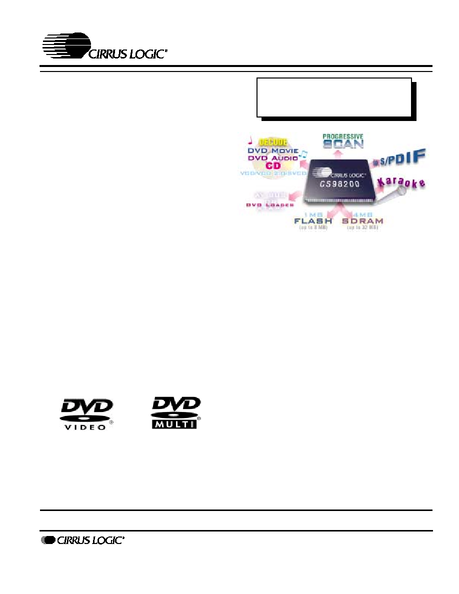
New Highly-Integrated Processor
for Tomorrow's DVD Players
and DVD Receivers
(cont.)
CS98200 Data Sheet
Preliminary Product Information
This document contains information for a new product.
Cirrus Logic reserves the right to modify this product without notice.
FEATURES
s DVD-Video, VCD, VCD 2.0, SVCD, CD, and other
popular standards
s DVD-Audio including CPPM and Verance
TM
watermark protection
s MPEG-1, MPEG-2, and leading edge MPEG-4 audio
and video decoding
s Kodak Picture CD
s Flexible ATAPI or AV bus DVD loader support with
no additional logic
s Dual 32-bit RISC processors, supported by RTOS,
C/C++ compilers, and source level debuggers
s 32-bit DSP capable of running AC-3, MPEG, DTS,
MP3, WMA, and AAC audio decode algorithms
s High quality integrated video encoder with six 10-bit
video D/A converters
s Component (RGB or YUV) or composite & S-Video
output
s Interlaced (PAL/NTSC) or progressive (480p) output,
with Macrovision
TM
copy protection
s CCIR656 video I/O for video capture, PVR and DVR
type applications, picture-in-picture support
s IEC60958/937 (S/PDIF) & simultaneous PCM output
s 5.1 downmix, karaoke echo mix, pitch shift, and many
other effects
s PAL / NTSC transcoding
s Dual 16550 compatible UARTs
s ATAPI/ IDE interface for hard disk, audio server, and
Personal Video Recorder (PVR) applications
s 240-pin MQFP package
ORDERING INFORMATION:
CS98200-CM
See ordering information legend on
page 60
.
OVERVIEW
CS98200 is a highly-integrated processor that provides all
of the audio and video processing functions needed for
the next generation of feature-rich DVD players, DVD
receivers and Internet DVD applications. Tomorrow's
features available today in a single chip solution are
DVD-Audio, MP3, WMA
�
, MPEG-2/4: AAC, Kodak
Picture CD
TM
, Dolby Digital
TM
, Dolby ProLogic II
TM
, and
DTS Digital Surround
TM
decoding. It supports most
popular CD formats, DVD navigation, disk control,
video decoding and up to eight channels of audio output.
An extension of Cirrus' CS98000 DVD product line, the
CS98200 integrates six 10-bit video digital-to-analog
converters (DACs) and TV encoding with progressive
scan functionality. Progressive scan video provides high
resolution and eliminates the "flickering" effect present in
traditional video playback. Other features enabled by
this integrated chip include karaoke functionality and
video special effects. Its extended feature set makes it
ideal for your next innovative DVD application ... today.
Need to get your product to market quickly? Cirrus'
Total Entertainment platform solutions include DVD
front-end controllers, MPEG encoders, audio DSPs, and
digital power amplifiers ... everything you need to
launch your product before the competition. CS98200 is a
Cirrus Total Entertainment Total-E
TM
IC solution
specifically designed for consumer entertainment
electronics.

2
Copyright 2002 Cirrus Logic (All Rights Reserved)
DS581PP2
CS98200
Next Generation DVD Processor
OVERVIEW
(cont.)
Here is a summary of the CS98200 features.
System Characteristics
� Dual 32-bit (180 MHz) RISC processors
� 32-bit DSP processor ~ 180 MIPS
� 240-pin MQFP package
� All I/O pins are 3 V with 5 V tolerance
� Advanced 0.18 � CMOS technology
� Low power modes and clock shutoff
Memory Controller
� Up to 120 MHz SDRAM from 4 MB to 32 MB
� FLASH databus isolated from SDRAM bus to allow
faster SDRAM access
� 32-bit data bus for DRAM, 8-bit data bus for ROM
data flow engine
� Two DMA controllers -- local memory based and
direct memory-to-memory
� DMA to/from main RAM into local SRAM
MPEG Video Decoder
� DVD, VCD, VCD 2.0 and SVCD
� MPEG-1, MPEG-2, and MPEG-4 simple profile
� Anti-tearing logic controls picture decode and
presentation
� Advanced error concealment hardware
Audio Interface
� 8 channels PCM output at 24-bits/192 kHz output
rate
� 2 channels I2S input at 24-bits/96 kHz
� IEC 60958/61937 capabilities
External Interface
� Serial master/slave ports for controlling DVD device
� ATAPI/IDE interface can also control hard disk
drives for PVR features
� Programmable bidirectional I/O pins
� All pins not used for other functions can be
reassigned as general purpose I/O pins
� Hardware assisted support for infrared remote
devices, such as remote control, infrared keyboard,
mouse, printer, and more
� Programmable parallel host master interface supports
formats including ATAPI, ISA, and more
� I/O channel interface supports all DVD loader
protocols
Video Processor
� OSD module with multiple regions and
transparencies
� Full screen graphics module, with 16 bit true-color
graphics plane
� High quality video scaling using multi-tap
programmable vertical and horizontal filters
Video Encoder
� Six 10-bit video DAC's, drives 37.5
load directly
� Progressive (480p) or interlaced PAL (B, D, G, H, I, N,
M, 60) and NTSC mode output
� Component (RBG or YUV) or composite + S-Video
output
� Macrovision
TM
7.1 support (interlaced) and
Macrovision
TM
1.03 support (progressive)
� Wide-screen signaling support (interlaced and
progressive) and CGMS
� Closed captioning support
DS581PP2
Copyright 2002 Cirrus Logic (All Rights Reserved)
3
CS98200
Next Generation DVD Processor
R IS C 0
R IS C 1
D S P
Au d io
In terfa ce
In stru ction
C ach e
D ata
C ach e
C PU Pipe
M A C
In stru ction
C ach e
D ata
C ach e
M A C
C PU Pipe
C PU /M A C
In stru ction
C ach e
X,Y D ata
M e m o ry
PC M O u t
PC M In
SP D IF O u t
D V D L o ad er I/O
M P E G D ec o d er
VL C
Pa rser
M o tion
C om p
ID C T
R AM
D VD C ustom L oad er
Pa ralle l/Se ria l Da ta
Se ria l C on tro l
AT AP I/G en eric
Pa ralle l Bu s Interfa ce
H o s t B u s I/O
D ata flo w
E n g in e
S ys tem C o n tro ls
N T S C /P A L E n co d er
V id e o P ro ce ss o r
S u b p ic tu re
S R A M + C P U IF
S ys tem S yn c
S im p le I/O
D R AM
C o n tro lle r
V id e o C ap tu re
G rap h ics
D M A (R d + W r)
FL AS H
M em ory.C o ntrol
ST C
Sch ed ule
D M A (2)t
SR A M Bu ffer
D ecryptio n
M isc.
R eg ister
Ba nks
In te rrup t
PL L
PL L
Tim e rs
D ig ital
En cod in g
3 D AC s
3 D AC s
32 K Byte
In te rna l
SR A M
Arb iter
+
C on tro l
D M A
D eco de
r
Sca le r
Line B uffe r
O n Scre en D ispla y O ve rla y
M a in V id eo
Sca ling a nd D ispla y
Pictu re in P icture O ve rla y
Line B uffe r / F licke r F ilte r
M a in G ra ph ics
D eco de r
FIFO
SD R A M C on tro l
Vide o M ixin g
D ua l U AR T
PW M S em i-D A C
2-W ire Se ria l (I
2
C )
3/4 W ire S erial (SP I)
Pro gra m m ab le I/O
In fra red Inp ut
PL L
M P E G 4 V id eo
D ec o d er Ac ce lera to r
C PU In te rfa ce
AL U + log ic
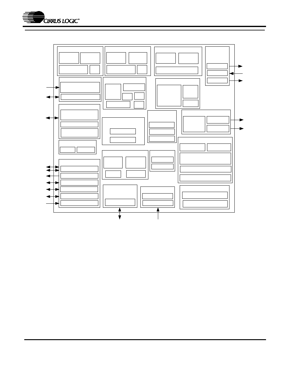
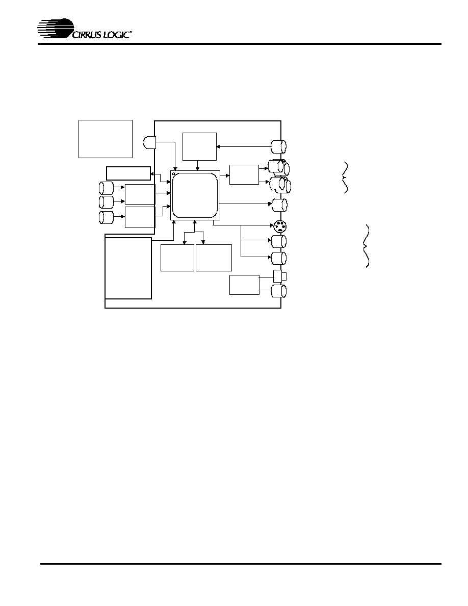
BLOCK DIAGRAM

4
Copyright 2002 Cirrus Logic (All Rights Reserved)
DS581PP2
CS98200
Next Generation DVD Processor
Table of Contents
1. CHARACTERISTICS AND SPECIFICATIONS ........................................................................ 8
1.1 AC and DC Parametric Specifications ...............................................................................8
1.1.1 Absolute Maximum Rating .................................................................................... 8
1.1.2 Recommended Operating Conditions ...................................................................8
1.1.3 Electrical Characteristics ......................................................................................8
2. TIMINGS .................................................................................................................................. 10
2.1 Timing Diagram Conventions ........................................................................................... 10
2.2 DC Characteristics ........................................................................................................... 11
2.2.1 ATAPI Interface ................................................................................................... 11
2.2.2 DVD Loader Interface ......................................................................................... 12
2.2.3 DVD Serial Interface Timing ................................................................................ 15
2.2.4 SDRAM Interface ................................................................................................ 16
2.2.5 ROM/NVRAM Interface ....................................................................................... 18
2.2.6 Digital Video Output Interface ............................................................................. 20
2.2.7 Video Input Interface ........................................................................................... 21
2.2.8 Audio Input Interface Timing ............................................................................... 22
2.2.9 Audio Output Interface Timing ............................................................................. 23
2.2.10 Miscellaneous Timings ...................................................................................... 24
3. TYPICAL APPLICATION ........................................................................................................ 25
4. CS98200 DEVICE SUMMARY ................................................................................................ 26
4.1 Block Diagram .................................................................................................................. 26
Contacting Cirrus Logic Support
Fo r a ll pro du ct qu es tio ns a nd in qu iries con tac t a C irrus L og ic S ales R e pre se ntative .
To find on e n ea rest yo u g o to
http://www.cirrus.com /corporate/contacts/sales.cfm
IMPORTANT NOTICE
"Preliminary" product information describes products that are in production, but for which full characterization data is not yet available. "Advance" product information
describes products that are in development and subject to development changes. Cirrus Logic, Inc. and its subsidiaries ("Cirrus") believe that the information contained in
this document is accurate and reliable. However, the information is subject to change without notice and is provided "AS IS" wit hout warranty of any kind (express or
implied). Customers are advised to obtain the latest version of relevant information to verify, before placing orders, that information being relied on is current and complete.
All products are sold subject to the terms and conditions of sale supplied at the time of order acknowledgment, including those pertaining to warranty, patent infringement,
and limitation of liability. No responsibility is assumed by Cirrus for the use of this information, including use of this infor mation as the basis for manufacture or sale of
any items, or for infringement of patents or other rights of third parties. This document is the property of Cirrus and by furnishing this information, Cirrus grants no license,
express or implied under any patents, mask work rights, copyrights, trademarks, trade secrets or other intellectual property rights. Cirrus owns the copyrights of the infor-
mation contained herein and gives consent for copies to be made of the information only for use within your organization with respect to Cirrus integrated circuits or other
parts of Cirrus. This consent does not extend to other copying such as copying for general distribution, advertising or promotional purposes, or for creating any work for
resale.
An export permit needs to be obtained from the competent authorities of the Japanese Government if any of the products or techno logies described in this material and
controlled under the "Foreign Exchange and Foreign Trade Law" is to be exported or taken out of Japan. An export license and/or quota needs to be obtained from the
competent authorities of the Chinese Government if any of the products or technologies described in this material is subject to the PRC Foreign Trade Law and is to be
exported or taken out of the PRC.
CERTAIN APPLICATIONS USING SEMICONDUCTOR PRODUCTS MAY INVOLVE POTENTIAL RISKS OF DEATH, PERSONAL INJURY, OR SEVERE PROPERTY OR
ENVIRONMENTAL DAMAGE ("CRITICAL APPLICATIONS"). CIRRUS PRODUCTS ARE NOT DESIGNED, AUTHORIZED, OR WARRANTED TO BE SUITABLE FOR
USE IN LIFE-SUPPORT DEVICES OR SYSTEMS OR OTHER CRITICAL APPLICATIONS. INCLUSION OF CIRRUS PRODUCTS IN SUCH APPLICATIONS IS UNDE R-
STOOD TO BE FULLY AT THE CUSTOMER'S RISK.
Cirrus Logic, Cirrus, and the Cirrus Logic logo designs are trademarks of Cirrus Logic, Inc. All other brand and product names i n this document may be trademarks or
service marks of their respective owners.
Purchase of I
2
C components of Cirrus Logic, Inc., or one of its sublicensed Associated Companies conveys a license under the Phillips I
2
C Patent Rights to use those com-
ponents in a standard I
2
C system
Microsoft
�
and Windows Media Technology
TM
are registered trademarks or trademarks of Microsoft, Inc. in the United States and/or other countries.
. HDCD
�
,
High Definition Compatible Digital
�
and Pacific Microsonics
TM
Inc. are either registered trademarks or trademarks of Pacific Microsonics Inc. in the United States and/or
other countries. HDCD technology provided under license from Pacific Microsonics Inc. This products design (and/or software) is covered by one or more of the following:
5,479,168; 5,638,074; 5,640,161; 5,808,574; 5,838,274; 5,854,600; 5,864,311; 5,872,531 with other patents pending.
Dolby Digital, AC-3, Dolby Pro Logic, Dolby Pro Logic II, Dolby Surround, Surround EX, Virtual Dolby Digital and the "AAC" logo are trademarks and the "Dolby Digital"
logo, "Dolby Digital with Pro Logic II" logo, "Dolby" and the double-"D" symbol are registered trademarks of Dolby Laboratories Licensing Corporation. DTS, DTS Digital
Surround, DTS-ES Extended Surround, DTS Neo:6, and DTS Virtual 5.1 are trademarks and the "DTS", "DTS-ES", "DTS Virtual 5.1" logos are registered trademarks of the
Digital Theater Systems Corporation. The "MPEG Logo" is a registered trademark of Philips Electronics N. V. Home THX Cinema and THX are registered trademarks of
Lucasfilm Ltd. Surround EX is a jointly developed technology of THX and Dolby Labs, Inc. AAC (Advanced Audio Coding) is an "MPEG-2-standard-based" digital audio
compression algorithm (offering up 5.1 discrete decoded channels for this implementation) collaboratively developed by AT&T, the Fraunhofer Institute, Dolby Laborato-
ries, and the Sony Corporation. In regards to the MP3 capable functionality of the CS98XXX Family DSP (via downloading of mp3_49 3xxx_vv.ld and mp3e_493xxx_vv.ld
application codes) the following statements are applicable: "Supply of this product conveys a license for personal, private and non-commercial use. MPEG Layer III audio
decoding technology licensed from Fraunhofer IIS and THOMSON Multimedia."

DS581PP2
Copyright 2002 Cirrus Logic (All Rights Reserved)
5
CS98200
Next Generation DVD Processor
4.2 CS98200 Device Details .................................................................................................. 26
4.2.1 RISC-32 Processors ........................................................................................... 26
4.2.2 Powerful 24/32-Bit DSP ...................................................................................... 26
4.2.3 System Controls .................................................................................................. 26
4.2.4 Memory Controller .............................................................................................. 26
4.2.5 Data Flow Engine ................................................................................................ 27
4.2.6 MPEG Video Decoder ......................................................................................... 27
4.2.7 System Synchronization ..................................................................................... 27
4.2.8 Audio Interface .................................................................................................... 27
4.2.9 Video Input .......................................................................................................... 27
4.2.10 External Interface .............................................................................................. 27
4.2.11 Video Processor ................................................................................................ 27
4.2.12 Sub-Picture Processor ...................................................................................... 27
4.2.13 Graphics Engine ............................................................................................... 27
4.2.14 On Screen Display Module ............................................................................... 28
4.2.15 DVD Loader Interface ....................................................................................... 28
4.2.16 CPU Interface and SRAM Controller ................................................................ 28
4.2.17 Host Bus Interface ............................................................................................ 28
4.2.18 Video Encoder .................................................................................................. 28
4.2.19 System Functions ............................................................................................. 28
5. FUNCTIONAL DESCRIPTION ............................................................................................... 29
5.1 RISC Processor ............................................................................................................... 29
5.2 DSP Processor ................................................................................................................ 29
5.3 Memory Control ............................................................................................................... 29
5.4 Dataflow Control (DMA) ................................................................................................... 29
5.5 System Control Functions ............................................................................................... 29
5.6 DVD/ATAPI Interface ....................................................................................................... 30
5.7 Serial DVD Interface ........................................................................................................ 30
5.8 MPEG Video Decoding .................................................................................................... 30
5.9 Audio Processing ............................................................................................................. 30
5.10 Video Encoder with Progressive Video DACs ............................................................... 32
5.11 Video Input/Output Interface .......................................................................................... 33
5.12 Universal Asynchronous Receiver/Transmitters (UARTs) ............................................. 34
6. MEMORY MAP ....................................................................................................................... 35
6.1 Processor Memory Map .................................................................................................. 35
7. 240-PIN MQFP PIN DESCRIPTION ....................................................................................... 36
7.1 240-Pin MQFP Pin Layout ............................................................................................... 36
7.2 240-Pin MQFP Pin Summary .......................................................................................... 37
7.3 Pin Configuration Summary ............................................................................................. 37
7.4 Explanation of Pin Types ................................................................................................. 38
7.5 240-Pin MQFP Pin Assignments ..................................................................................... 38
8. INTERFACE DESCRIPTIONS ................................................................................................ 49
8.1 SDRAM Interface Pins ..................................................................................................... 49
8.2 ROM/NVRAM Interface Pins ........................................................................................... 49
8.3 Video Output Interface Pins ............................................................................................. 50
8.4 Video Input Interface Pins ............................................................................................... 50
8.5 Audio PCM Interface Pins ............................................................................................... 51
8.6 Host Master/ATAPI Interface ........................................................................................... 52
8.7 DVD Loader Interface ...................................................................................................... 53
8.8 DVD Serial Data Interface ............................................................................................... 53
8.9 SPI Interface .................................................................................................................... 54
8.10 General Purpose Input/Output (GPIO) .......................................................................... 54
8.11 UART Interface Pins ...................................................................................................... 55
8.12 I
2
C Interface .................................................................................................................. 55
8.13 Miscellaneous Interface Pins ......................................................................................... 55

6
Copyright 2002 Cirrus Logic (All Rights Reserved)
DS581PP2
CS98200
Next Generation DVD Processor
8.14 Power and Ground ......................................................................................................... 56
9. 240-PIN MQFP PACKAGE SPECIFICATIONS ...................................................................... 57
10. CONVENTIONS .................................................................................................................... 58
10.1 Acronyms and Abbreviations ......................................................................................... 58
10.2 Units of Measurement .................................................................................................... 59
10.3 General Conventions ..................................................................................................... 59
10.4 Pin Description Conventions .......................................................................................... 60
11. ORDERING INFORMATION LEGEND ................................................................................. 60
List of Figures
Figure 1. Legend for Timing Diagrams .......................................................................................... 10
Figure 2. ATAPI Interface Timing Diagram.................................................................................... 11
Figure 3. DVD Loader Host Interface ............................................................................................ 12
Figure 4. DVD Loader Data Interface ............................................................................................ 13
Figure 5. DVD Loader CD Interface .............................................................................................. 13
Figure 6. DVD Loader CD Interface Formats ................................................................................ 14
Figure 7. DVD Serial Interface Timing ........................................................................................... 15
Figure 8. SDRAM Refresh Transaction ......................................................................................... 16
Figure 9. SDRAM Burst Write Transaction.................................................................................... 16
Figure 10. SDRAM Burst Read Transaction.................................................................................. 17
Figure 11. SDRAM Timing............................................................................................................. 17
Figure 12. ROM/NVRAM Reading Timing ..................................................................................... 18
Figure 13. ROM/NVRAM Write Timing.......................................................................................... 19
Figure 14. CS98200 Digital Video Interface Timing Diagram ........................................................ 20
Figure 15. Video Input Timing ....................................................................................................... 21
Figure 16. Audio Input Timings...................................................................................................... 22
Figure 17. Digital Audio Out Timing Diagram ................................................................................ 23
Figure 18. Miscellaneous Timings ................................................................................................. 24
Figure 19. CS98200 Typical Application ....................................................................................... 25
Figure 20. CS98200 Block Diagram .............................................................................................. 26
Figure 21. Video DAC Connections............................................................................................... 32
Figure 22. UART Data Transfer..................................................................................................... 34
Figure 23. 240-Pin MQFP Pin Layout............................................................................................ 36
Figure 24. 240-Pin MQFP Pinout Summary .................................................................................. 37
Figure 25. 240-Pin MQFP Package Drawing ................................................................................ 57
List of Tables
Table 1. ATAPI Interface Characteristics ...................................................................................... 11
Table 2. SDRAM Interface Characteristics .................................................................................... 16
Table 3. RAM/NVROM Characteristics ......................................................................................... 18
Table 4. CS98200 Digital Video Interface Characteristics............................................................. 20
Table 5. Video Input Interface Symbols and Characterization Data .............................................. 21
Table 6. Audio Input Interface Symbols and Characterization Data .............................................. 22
Table 7. Digital Audio Out Characteristics ..................................................................................... 23
Table 8. Miscellaneous Timing Characteristics ............................................................................. 24
Table 9. Memory Map-RISC0 Processor....................................................................................... 35
Table 10. Host Debug Port Address Map...................................................................................... 35
Table 11. DSP Address Map ......................................................................................................... 35
Table 12. Pin Configuration Summary........................................................................................... 37
Table 13. Pin Type Legend ........................................................................................................... 38
Table 14. 240-Pin MQFP Pin Assignments ................................................................................... 38

DS581PP2
Copyright 2002 Cirrus Logic (All Rights Reserved)
7
CS98200
Next Generation DVD Processor
Table 15. SDRAM Interface Pins .................................................................................................. 49
Table 16. ROM/NVRAM Interface................................................................................................. 49
Table 17. Video Output Interface .................................................................................................. 50
Table 18. Video Input Interface ..................................................................................................... 50
Table 19. PCM Audio Interface ..................................................................................................... 51
Table 20. Host Master/ATAPI Interface ........................................................................................ 52
Table 21. DVD I/O Channel Interface ........................................................................................... 53
Table 22. SPI Interface ................................................................................................................. 54
Table 23. General Purpose I/O Interface ...................................................................................... 54
Table 24. UART Interface Pins ..................................................................................................... 55
Table 25. I
2
C Interface Pins .......................................................................................................... 55
Table 26. Miscellaneous Interface Pins ........................................................................................ 55
Table 27. Power and Ground ........................................................................................................ 56
Table 28. Acronyms and Abbreviations ........................................................................................ 58
Table 29. Units of Measurement ................................................................................................... 59
Table 30. Pin Description Conventions ......................................................................................... 60

8
Copyright 2002 Cirrus Logic (All Rights Reserved)
DS581PP2
CS98200
Next Generation DVD Processor
1.
CHARACTERISTICS AND SPECIFICATIONS
1.1
AC AND DC PARAMETRIC SPECIFICATIONS
(AGND, DGND=0 V, all voltages with respect to 0 V)
1.1.1
ABSOLUTE MAXIMUM RATING
CAUTION: Operating beyond these Minimum and Maximum limits can result in permanent dam-
age to the device. Cirrus Logic recommends that CS98200 devices operate at the settings described
in the next table.
1.1.2
RECOMMENDED OPERATING CONDITIONS
1.1.3
ELECTRICAL CHARACTERISTICS
Symbol
Description
Min
Max
Unit
VDD
IO
Power Supply Voltage on analog core and I/O ring
-0,5
4.6
Volts
VDD
CORE
Power Supply Voltage on core logic and PLL
-0.5
2.5
Volts
V
I
Digital Input Applied Voltage (power applied)
-0.5
5.5
Volts
I
I
Digital Input Forced Current
-10
10
mA
I
O
Digital Output Forced Current
-50
50
mA
T
SOL
Lead Soldering Temperature
-
260
o
C
T
VSOL
Vapor Phase Soldering Temperature
-
235
o
C
T
STOR
Storage Temperature (no power applied)
-40
125
o
C
T
AMB
Ambient Temperature (power applied)
0
70
o
C
P
total
Total Power consumption
-
2.2
W
Parameter
Symbol
Min
Typ
Max
Units
Supply Voltage, Analog and IO
V
IO
& V
AA
3.0
3.3
3.6
Volts
Supply Voltage, Core Logic and PLL
V
PLL &
V
DD
1.62
1.8
1.98
Volts
Ambient Temperature (power applied)
T
AMB
0
25
70
o
C
Parameter
Symbol
Conditions
Min
Typ
Max
Units
Supply Current, IO
I
DD
Normal Operating
65
mA
Supply Current, Core Logic and
PLL
I
DD
Normal Operating
210
mA
Input Voltage, High
V
IH
2.0
-
Volts
Input Voltage, Low
V
IL
-
-
0.8
Volts
Input Current
I
IN
V
IN
= V
DD
or V
SS
-1
-
1
�
A
Input Pull up/down resistor
R
I
-
75
-
K
Output Voltage, High
V
OH
@ buffer rating
2.2
-
-
Volts
Output Voltage, Low
V
OL
@ buffer rating
-
-
0.4
Volts
High-Z-state Leakage
I
OZ
V
OUT
= V
SS
or V
DD
-1
-
1
�
A
Video DACs
1
R
SET
= 174
DAC Resolution
10
bits
DAC to DAC matching
2
MAT
2
%
Output Voltage Range
V
out
R
LOAD
= 37.5
3
1.28
Volts

DS581PP2
Copyright 2002 Cirrus Logic (All Rights Reserved)
9
CS98200
Next Generation DVD Processor
Differential Gain
DG
1
%
Differential Phase
DP
0.5
%
Signal to Noise
SNR
74
dB
Chrominance AM Noise
AM
80
dB
Chrominance PM Noise
PM
75
dB
1.
Video parameters guaranteed only with 1% tolerance resistors or better for Rset and RLoad.
2.
Only applies to each set of three DACs.
3.
RLoad is a double terminated load, which includes a 75
resistor at the video DAC and a 75
resistor at the video monitor.
10
Copyright 2002 Cirrus Logic (All Rights Reserved)
DS581PP2
CS98200
Next Generation DVD Processor
2. TIMINGS
2.1
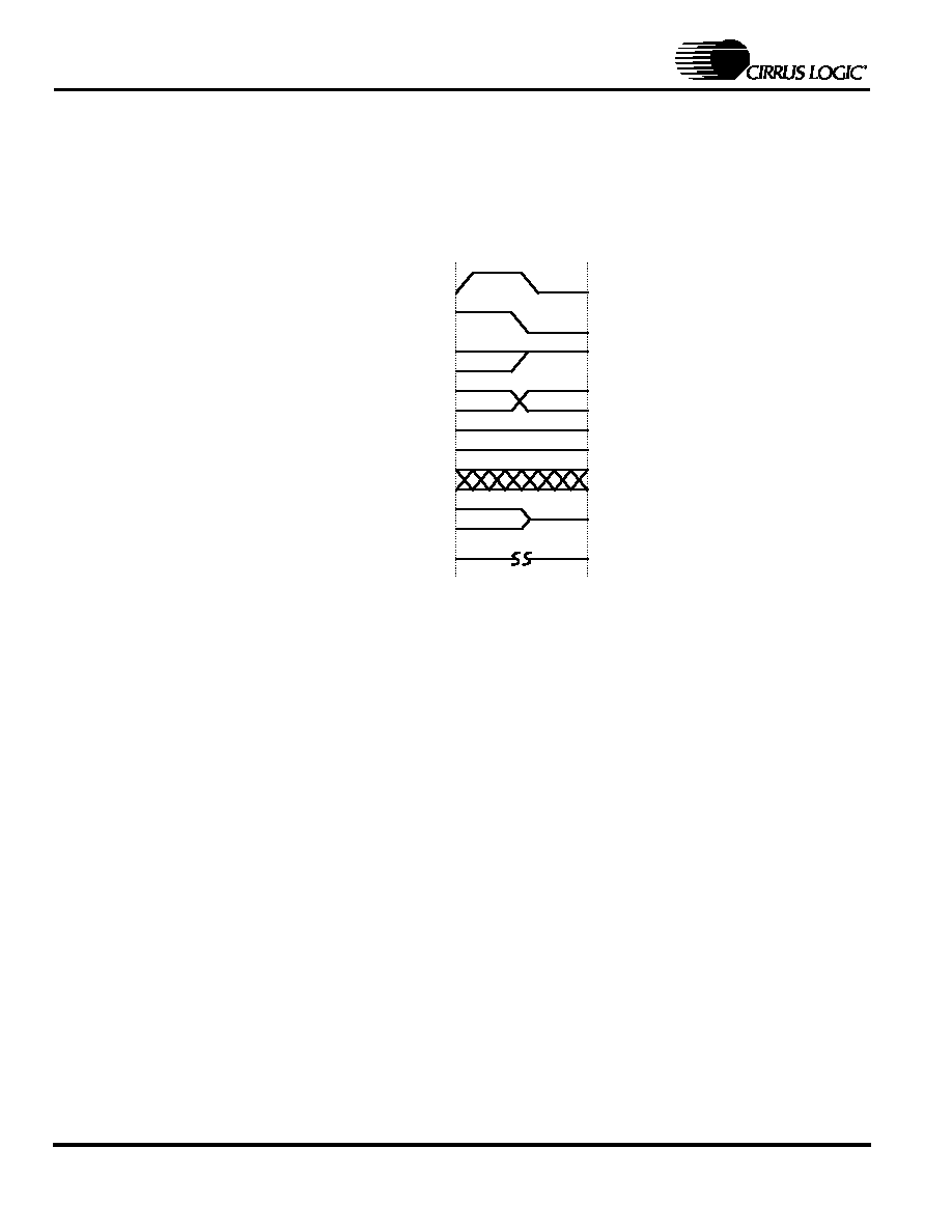
Timing Diagram Conventions
This data sheet contains timing diagrams. The following key explains the components used in
these diagrams. Any variations are clearly labeled when they occur. Therefore, no additional
meaning should be attached unless specifically stated.
C l o c k
H i g h t o L o w
H i g h / L o w t o H i g h
B u s C h a n g e
B u s V a l i d
U n d e f i n e d / I n v a l i d
V a l i d B u s t o T r i s t a t e
B u s / S i g n a l O m i s s i o n
Figure 1. Legend for Timing Diagrams
DS581PP2
Copyright 2002 Cirrus Logic (All Rights Reserved)
11
CS98200
Next Generation DVD Processor
2.2
DC CHARACTERISTICS
(
T
A
= 25� C; V
PLL
=V
DD
=1.8V�10%, V
IO
=V
AA
=3.3 V�10%)
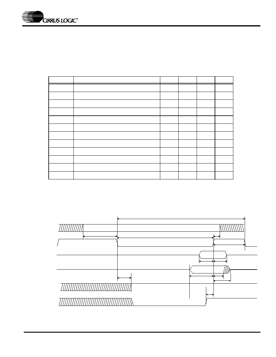
2.2.1
ATAPI Interface
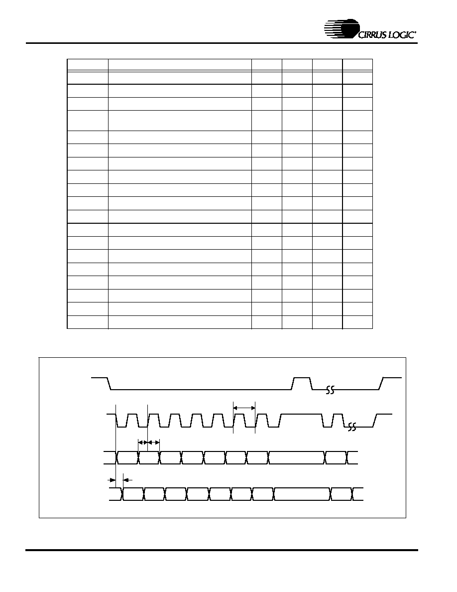
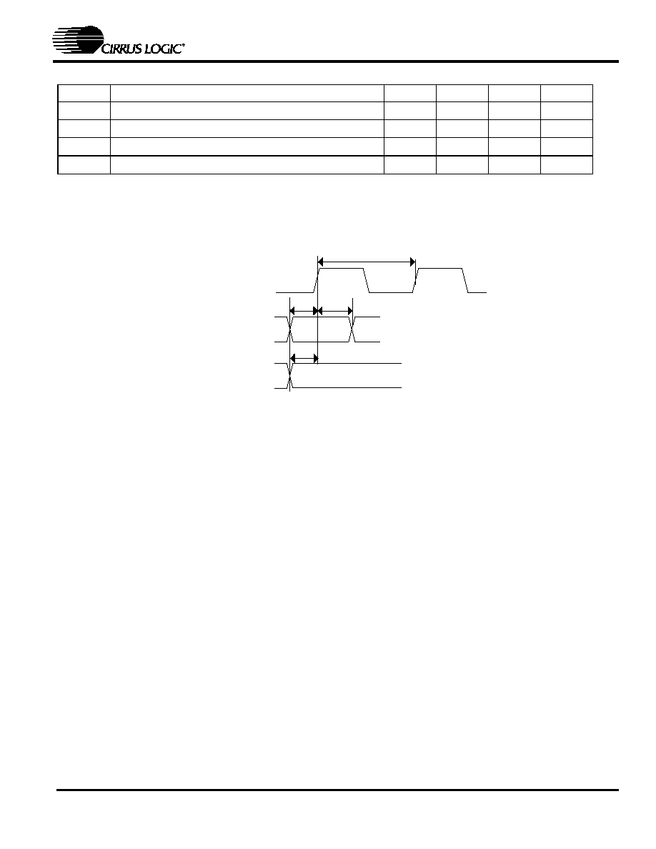
CS98200 can interface with a ATAPI-type slave loader gluelessly.
Figure 2
illustrates a read ATAPI
transaction and a write ATAPI transaction.
Symbol
Description
Min
Typ
Max
Unit
t
acyc
1
1.
Values are guaranteed by design only
Cycle Time
87
ns
t
aavr
Address Valid to HMRD-/HMWR- Setup
7
ns
t
ah
Address Hold from HMRD-/HMWR Setup
11
ns
t
arww
H_RD/H_WR Pulse Width
63
ns
t
arec
H_RD/H_WR Recovery Time
21
ns
t
awsu
H_WR Data Setup
30
ns
t
awh
H_WR Data Hold
8
ns
t
ardsu
H_RD Data Setup
20
ns
t
arddh
H_RD Data hold
0
ns
t
ardts
H_RD Data High-Z-state
8
ns
t
arsu
H_RDY Setup Time
14
ns
t
arh
1
H_RDY Hold Time
0
ns
Table 1. ATAPI Interface Characteristics
H_A[2:0] ,
H_CS[3:0]
H_D[15:0](WRITE)
H_D[15:0](READ)
H_RD/H_WR
t
acyc
t
aavr
t
arww
t
ah
t
arec
t
arsu
t
awh
t
awsu
t
ardsu
t
arddh
t
ardts
t
arh
H_RDY(deasserted
before tarsu)
H_RDY(asserted
before tarsu)
Figure 2. ATAPI Interface Timing Diagram
12
Copyright 2002 Cirrus Logic (All Rights Reserved)
DS581PP2
CS98200
Next Generation DVD Processor
2.2.2
DVD Loader Interface
Symbol
Description
Min
Typ
Max
Unit
t
dlckper
DVDL_CK Period
400
ns
t
dldisu
DVDL_DI Setup Time
5
ns
t
dldih
DVDL_DI Hold Time
10
ns
t
dldod
DVDL_DO Output Delay from Falling
Edge
5
ns
t
dlstbwd
DVD_STB Width
250
ns
t
dlstbl
DVD_STB Low Time
40
%
t
dlstbh
DVD_STB High Time
40
%
t
dlreqod
DVD_RDY Output Delay
90
ns
t
dlensu
DVD_ENA Setup Time
5
ns
t
dlenh
DVD_ENA Hold Time
5
ns
t
dldsu
DVD_D[7:0] Setup Time
5
ns
t
dldh
DVD_D[7:0] Hold Time
5
ns
t
dlsossu
DVD_SOS Setup Time
5
ns
t
dlsosh
DVD_SOS Hold Time
5
ns
t
lrcksu
CD_LRCK Setup Time
5
ns
t
cddsu
CD_DATA Setup Time
5
ns
t
cddh
CD_DATA Hold Time
5
ns
t
cdcpsu
CD_C2PO Setup Time
5
ns
t
cdcph
CD_C2PO Hold Time
5
ns
Figure 3. DVD Loader Host Interface
D VD L -C K
(O u tpu t)
D VD L _R D Y
(Inp ut)
D VD L _D I
(Inp ut)
D VD L _D O
(O u tpu t)
D 0
D 1
D 2
D 3
D 4
D 5
D 6
D 7
D 0
D 1
D 2
D 3
D 4
D 5
D 6
D 7
t
dlckper
t
dldisu
t
dldih
t
dldo d

DS581PP2
Copyright 2002 Cirrus Logic (All Rights Reserved)
13
CS98200
Next Generation DVD Processor
Figure 4. DVD Loader Data Interface
D V D _R E Q
(O utp u t)
D V D _S T B
(In p ut)
D V D _E N A
(In p ut)
D V D _D [7:0 ]
(In p ut)
D V D _S O S
(In p ut)
D V D _E R R
(In p ut)
t
d lstbw d
t
d lstbl
t
d lstbh
t
d lre qo d
t
d le nsu
t
d le nh
t
d ld su
t
d ld h
t
d lso ssu
t
d lso sh
Figure 5. DVD Loader CD Interface
C D _ B C LK (Inp ut)
C D _ D A T A (Inp ut)
C D _ L R C K (In p ut)
C D _ C 2P O (Inp ut)
t
lrcksu
t
cddsu
t
cddh
t
c2poh
t
c2posu

14
Copyright 2002 Cirrus Logic (All Rights Reserved)
DS581PP2
CS98200
Next Generation DVD Processor
Figure 6. DVD Loader CD Interface Formats
15
0
1
C D _ B C K
C D _ LR C K
D A T A
C 2 P 0
14 13 12 11 10 9
8
7
6
5
4
3
2
Invalid
0
15
0
1
14 13 12 11 10 9
8
7
6
5
4
3
2
In va lid
M S B
LSB
MSB
LS B
Lo wer (L eft Channel)
Upper (Left Channe l)
Lower (Right Channel)
Uppe r (Righ t Channel)
32-bit B C K , MS B First, R ig ht C han nel L ow , C 2P 0 LS B F irst, D a ta latch tim ing high
15
0
1
C D _ B C K
C D _ LR C K
D A T A
C 2 P 0
14 13 12 11 10 9
8
7
6
5
4
3
2
Invalid
0
15
0
1
14 13 12 11 10 9
8
7
6
5
4
3
2
In va lid
M S B
LSB
MSB
LS B
Up per (Right Channel)
Lower (Right Chann el)
Upper (Left Channel)
Lower (Left Cha nnel)
32-bit B C K , MS B First, Left C hann el L ow , C 2P 0 MS B F irst, D a ta latch tim ing lo w
15
0
1
C D _ B C K
C D _ LR C K
D A T A
C 2 P 0
14 13 12 11 10 9
8
7
6
5
4
3
2
Invalid
0
M SB
LS B
Lower (Left Channel)
Upper (Left Channe l)
Lower (Right Chan nel)
Upper (Righ t Chan nel)
24-bit B C K , MS B First, R ig ht C han nel L ow , C 2P 0 M S B F irst, D ata la tc h tim ing high
Left Channel
Righ t Channel
Right Ch annel
Le ft Channel
Left Channel
Righ t Channel
15
0
1
14 13 12 11 10 9
8
7
6
5
4
3
2
In va lid
M SB
LS B
15 14 13 12 11 10 9
8
7
6
5
Invalid
MSB
Upper (Left Channel)
Left Channel
C D _ B C K
C D _ LR C K
D A T A
C 2 P 0
Invalid
0
L SB
M SB
Lower (Left Channel)
Upper (Left Channe l)
Lower (Right Chan nel)
Upper (Righ t Chan nel)
24-bit B C K , LS B F irst, R ight C hann el L ow , C 2P 0 MS B F irst, D a ta latch tim ing lo w
Left Channel
Righ t Channel
In va lid
LSB
MS B
Invalid
LSB
Upper (Left Channel)
Left Channel
0
15
1
14
13
1 2
11
10
9
8
7
6
5
4
3
2
0
15
1
14
13
12
11
10
9
8
7
6
5
4
3
2
0
1
10
9
8
7
6
5
4
3
2
15
0
1
C D _ B C K
C D _ LR C K
D A T A
14 13 12 11 10 9
8
7
6
5
4
3
2
Invalid
0
M SB
LS B
2 4-bit B C K , M S B F irst, R ight C hanne l Low , D a ta latch tim ing high (N ote: no C 2P 0 for this fo r m at)
Left Channel
Righ t Channel
15
0
1
14 13 12 11 10 9
8
7
6
5
4
3
2
In va lid
M SB
LS B
15 14 13 12 11 10 9
8
7
6
5
Invalid
MSB
Left Channel
15
0
1
C D _ B C K
C D _ LR C K
D A T A
C 2 P 0
14 13 12 11 10 9
8
7
6
5
4
3
2
0
MS B
LSB
Lower (Left Cha nnel)
Upper (Left Channel)
Lower (Right Channel)
Upper (Right Channel)
16-bit B C K , MS B First, Left C hann el L ow , C 2P 0 LS B Firs t, D ata la tch ti m in g high
Left Ch annel
Right Channel
15
0
1
14 13 12 11 10 9
8
7
6
5
4
3
2
M S B
L SB
15
0
1
14 13 12 11 10 9
8
7
6
5
4
3
2
M SB
L SB
Lower (Left Channel)
Upper (Left Channel)
Lower (Right Chan nel)
Upper (Right Chan nel)
Left Ch annel
Righ t Chan nel
15
0
1
14 13 12 11 10 9
8
7
6
5
4
3
2
MSB
LSB
15 14 13
MSB
DS581PP2
Copyright 2002 Cirrus Logic (All Rights Reserved)
15
CS98200
Next Generation DVD Processor
2.2.3
DVD Serial Interface Timing
Symbol
Description
Min
Typ
Max
Unit
tdsckper
1
DVDS_CLK Period
33
ns
tdsckl
1
DVDS_CLK Low Time
40
50
%
tdsckh
1
DVDS_CLK High Time
40
50
%
tdsdsu
DVDS_DATA Setup to DVDS_CLK active edge
5
ns
tdsdhd
DVDS_DATA Hold after DVDS_CLK active edge 5
ns
tdscdsu
DVDS_VLD, DVDS_SOS Setup to DVDS_CLK
5
ns
tdscdhd
DVDS_VLD, DVDS_SOS Hold after DVDS_CLK 5
ns
1.
Values are guaranteed by design only
Figure 7. DVD Serial Interface Timing
D V D S_C L K
(Input)
D V D S_D A T A
(Input)
D V D S_V L D , D V D S_S O S
(Input)
dsckl
dsckh
dsdhd
dscdhd
dsckper
t
t
t
t
dsdsu
t
dscdsu
t
t
16
Copyright 2002 Cirrus Logic (All Rights Reserved)
DS581PP2
CS98200
Next Generation DVD Processor
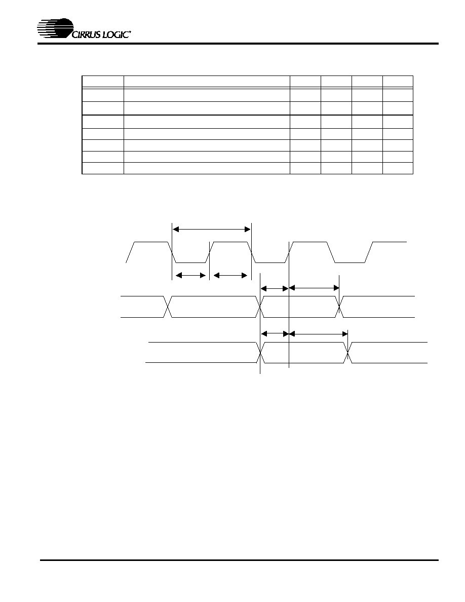
2.2.4
SDRAM Interface
CS98200 interfaces with either SDRAM or SGRAM for high data bandwidth transfer.
Figure 8
shows
the refresh cycle performed by CS98200.
Symbol
Description
Min
Typ
Max
Unit
t
mco
Output Delay from M_CKO active edge
9
ns
t
mper
M_CKO Period
8
ns
t
mdow
M_D[31:0] delay from M_CKO
9
ns
t
msur
M_D[31:0] setup to M_CKO
3
ns
t
mhr
M_D[31:0] hold time after M_CKO
2.5
ns
Table 2. SDRAM Interface Characteristics
M_CKO
M_A[10:0]
M_BS0_N,
M_RAS_N
M_CAS_N
M_W E_N
M_D[31:0]
M_DQM_[3:0]
M_AP
M_BS1_N
Figure 8. SDRAM Refresh Transaction
D 0
D 1
D 2
D 3
D 4
D 5
D 6
D 7
C 1
C 2
C 3
C 4
C 5
C 6
C 7
C 0
R 0
M _ C KO
M _ A_ [1 0:0]
M _ C KE
M _ R AS _N
M _ C AS _N
M _ W E_ N
M _ D [3 1:0]
M _ D Q M [3:0]
0
F
F
Figure 9. SDRAM Burst Write Transaction

DS581PP2
Copyright 2002 Cirrus Logic (All Rights Reserved)
17
CS98200
Next Generation DVD Processor
D 0
D 1
D 2
D 3
D 4
D 5
D 6
D 7
C 1
C 2
C 3
C 4
C 5
C 6
C 7
C 0
R 0
M _ C KO
M _ A_ [1 0:0]
M _ C KE
M _ R AS _N
M _ C AS _N
M _ W E_ N
M _ D [3 1:0]
M _ D Q M [3:0]
0
F
F
Figure 10. SDRAM Burst Read Transaction
M_RAS_N,M_CAS_N
M_WE_N,M_AP,M_DQM[3:0],
M_CKE,M_A[10:0]
t
mper
t
mco
M_D[31:0](WRITE)
M_D[31:0](READ)
M_CKO
t
msur
t
mhr
t
mdow
Figure 11. SDRAM Timing

18
Copyright 2002 Cirrus Logic (All Rights Reserved)
DS581PP2
CS98200
Next Generation DVD Processor
2.2.5
ROM/NVRAM Interface
Symbol
Description
Min
Typ
Max
Unit
t
rc
Read Cycle Time
75
ns
t
cds
CE to Data Setup
80
ns
t
ods
OE to Data Setup
70
ns
t
ads
Address to Data Setup
80
ns
t
aws
Address to WE setup (Write)
64
ns
t
cws
CE to WE setup (Write)
64
ns
t
wp
WE Pulse Width (Write)
160
ns
t
cdo
CE to Data Output (Write)
0
ns
t
dh
WE to Data Hold (Write)
10
ns
Table 3. RAM/NVROM Characteristics
Figure 12. ROM/NVRAM Reading Timing
N V_C E_N
N V_W E_N
N V_O E_N
(M _A P)
A ddress[22:0]
M _D [7:0]
t
rc
t
ads
t
cds
t
ods
DS581PP2
Copyright 2002 Cirrus Logic (All Rights Reserved)
19
CS98200
Next Generation DVD Processor
N V _ C E _ N
N V _ W E _ N
N V _ O E _ N
(M _ A P )
A d d r[2 2 :0 ]
M _ D [7 :0 ]
t
aw s
t
cw s
t
w dh
t
w p
t
cdo
Figure 13. ROM/NVRAM Write Timing

20
Copyright 2002 Cirrus Logic (All Rights Reserved)
DS581PP2
CS98200
Next Generation DVD Processor
2.2.6
Digital Video Output Interface
Figure 14
illustrates the signal timing for the digital video interface pins.
Symbol
Description
Min
Typ
Max
Unit
t
vocper
1
1.
Values are guaranteed by design only
XTLCLK period
37.037
ns
t
covo1
2
2.
It is recommanded that the output data should be taken at the opposite edge of the CLK27_O.
VDAT[7:0] delay from XTLCLK
-10
10
ns
t
covo2
2
Vsync/Hsync delay from XTLCLK
-10
10
ns
Table 4. CS98200 Digital Video Interface Characteristics
V o u t_ C L K
(O u tp u t)
V o u t_ D 7:0 ]
(O u tp u t)
V o u t_ H S /V o u t_V S
(O u tp u t)
t
vocper
t
covo1
t
covo2
Figure 14. CS98200 Digital Video Interface Timing Diagram
DS581PP2
Copyright 2002 Cirrus Logic (All Rights Reserved)
21
CS98200
Next Generation DVD Processor
2.2.7
Video Input Interface
.
Symbol
Description
Min
Typ
Max
Unit
t
vicper
Video Clock input period
37.037
ns
t
sutc1
VIN_D[7:0] setup time
5
ns
t
hvi
VIN_D[7:0] hold time
5
ns
t
sutc2
VIN_HS/VS setup time
5
ns
Table 5. Video Input Interface Symbols and Characterization Data
V IN _C L K
V IN _D [7 -0 ]
t
sutc1
t
hvi
t
vicper
V IN _H S ,V IN _ VS
t
sutc2
Figure 15. Video Input Timing
22
Copyright 2002 Cirrus Logic (All Rights Reserved)
DS581PP2
CS98200
Next Generation DVD Processor
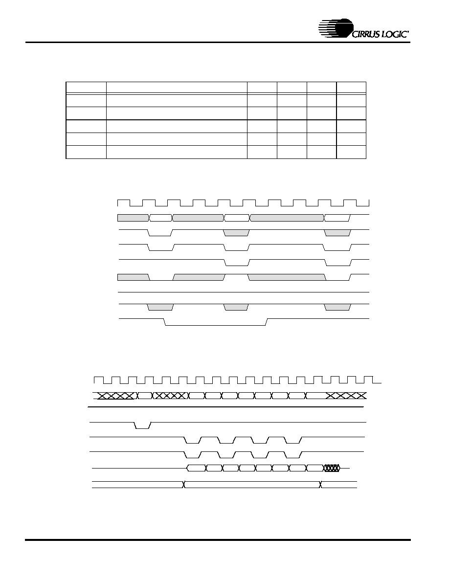
2.2.8
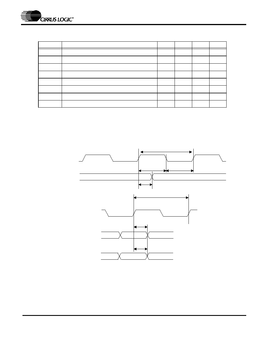
Audio Input Interface Timing
Symbol
Description
Min
Typ
Max
Units
t
aicl
AUDI_BCK Low Time
1,
2
1.
Values are guaranteed by design only
2.
Active clock edge is programmable. Timing is referenced from active edge
40
50
%
t
aich
AUDI_BCK High Time
1, 2
40
50
%
t
aiper
AUDI_BCK period
1, 2
80
ns
t
lrts
AUDI_LR setup time
5
-
ns
t
sdsus
AUDI_D setup time
5
-
ns
t
sdhs
AUDI_D hold time
5
-
ns
Table 6. Audio Input Interface Symbols and Characterization Data
Figure 16. Audio Input Timings
AUDI_BCK (Input)
AUDI_DATA (Input)
AUDI_LRCK (Input)
t
lrts
t
sdsus
t
sdhs
t
aich
t
aicl
t
aiper
DS581PP2
Copyright 2002 Cirrus Logic (All Rights Reserved)
23
CS98200
Next Generation DVD Processor
2.2.9
Audio Output Interface Timing
Figure 17
and
Figure 16
illustrate the signal timing for the digital audio pins.
Symbol
Description
Min
Typ
Max
Unit
t
axper
AUD_XCLK period (Input/Output)
1, 2
13
-
ns
t
axch
AUD_XCLK High Time (Input/Output)
1,
2
1.
Values are guaranteed by design only
2.
Active clock edge is programmable. Timing is referenced from active edge
40
50
%
t
axcl
AUD_XCLK Low Time (Input/Output)
1, 2
47
50
%
t
sdmo
AUDO_BCK delay from AUD_XCLK output rise
10
t
sdmi
AUDO_BCK delay from AUD_XCLK input rise
20
t
aoper
AUDO_BCK period (Output)
1, 2
104
t
lrds
AUDO_LR delay from AUDO_BCK output rise
-10
10
ns
t
adsm
AUDO_D[3:0] delay from AUDO_BCK output rise -10
10
ns
Table 7. Digital Audio Out Characteristics
Figure 17. Digital Audio Out Timing Diagram
AUDO_BCK(Output)
AUD_XCLK(Input/Output)
t
sdm
t
axch
AUDO_BCK(Output)
AUDO_DO[3:0] (Output)
AUDO_LR(Output)
t
lrds
t
adsm
t
axcl
t
axper
t
aoperl
24
Copyright 2002 Cirrus Logic (All Rights Reserved)
DS581PP2
CS98200
Next Generation DVD Processor
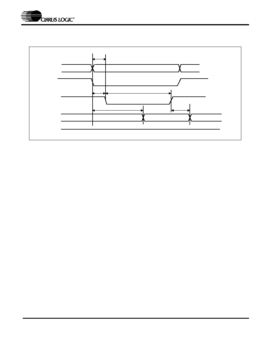
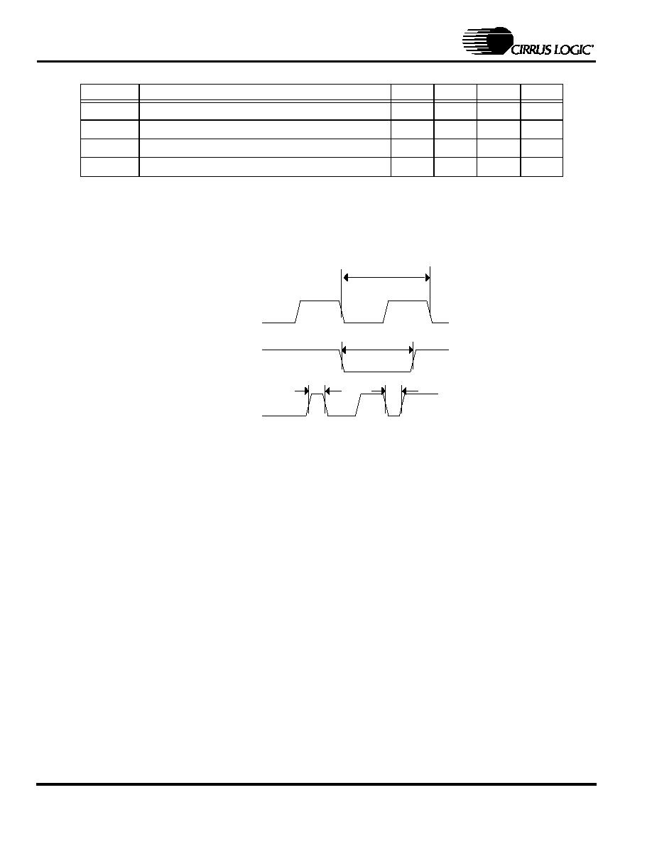
2.2.10
Miscellaneous Timings
Symbol
Description
Min
Typ
Max
Unit
t
xccper
1
1.
XTLCLK must meet the requirement of external the video encoder for correct chroma (27 MHz
�
1
KHz).
XTLCLK period
37.037
ns
t
rstl
RST_N Low Pulse Width
1000
ns
t
gph
GPIO PW High
50
ns
t
gpl
GPIO PW Low
50
ns
Table 8. Miscellaneous Timing Characteristics
RESET-N
t
gph
t
gpl
t
rstl
XTLCLOCK
GPIO
xccper
t
Figure 18. Miscellaneous Timings
DS581PP2
Copyright 2002 Cirrus Logic (All Rights Reserved)
25
CS98200
Next Generation DVD Processor
3. TYPICAL APPLICATION
The
Figure 19
shows a typical example of a complete DVD Receiver solution using the CS98200.
F L A S H
2 M
(U p to 8 M B)
S D R A M
8 M
(U p to 3 2 M B)
..
.
.
D ig ita l
In te rf a c e
R e c e iv e r
IR
(4 )A u d io
D A C s
P o w e r
R e g .
A u d io
A D C
V id e o
D e c o d e r
F ro n t P a n e l
C S 9 82 00
S /P D IF In pu t
A u dio-L(4 )
A u dio-R (4 )
S -V ide o
C o m po site V ide o
S w itch
P o w er
C D L o a d e r
(A T A P I ,
A / V )
A u dio-L
A u dio-R
V ide o
C o m po nen t V id eo
6 V id eo D A C s
A u dio u p to
8 C ha nn els
S /P D IF O utpu t
R em ote
K eybo ard
C on trol
Figure 19. CS98200 Typical Application
26
Copyright 2002 Cirrus Logic (All Rights Reserved)
DS581PP2
CS98200
Next Generation DVD Processor
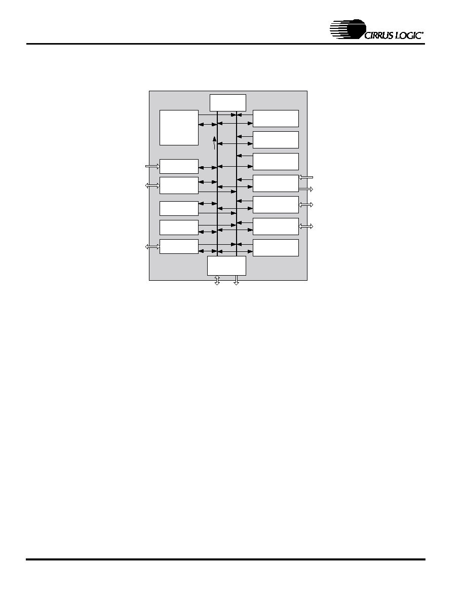
4. CS98200 DEVICE SUMMARY
4.1
Block Diagram
The CS98200 block diagram is shown in
Figure 20
.
4.2
CS98200 Device Details
4.2.1
RISC-32 Processors
� Two Powerful 32-bit RISC processors (RISC0
and RISC1), Generation III
� Virtual memory support
� Optimizing C compiler
� Big or little endian data formats support
� MAC multiply/accumulate in 2 cycles with
C support
� 4 Kbyte instruction cache, 2 Kbyte data
cache
� Single cycle instructions, runs at 180 Mhz
4.2.2
Powerful 24/32-Bit DSP
� Powerful 24/32-bit DSP processor
� 24-bit fixed point logic, with 54-bit accumu-
lator
� Single-cycle throughput, 2-cycle latency
multiply accumulate, 32-bit simple integer
logic. 8-Kbyte instruction cache
� Single cycle instructions, runs at 180 Mhz
� Expanded 4 Kbyte X + 16 KByte Y paged
program visible local memory, Total data
RAM = 20 KBytes
4.2.3
System Controls
� Includes several hardware lockable sema-
phore registers
� General-purpose register for inter-processor
communication
� 32-bit timers for I/O and other uses, with
programmable interval rates
� Both hardware and software interrupts on
data or debug
� Built in PLLs generate all required clocks
from 27 Mhz input clock
4.2.4
Memory Controller
� Supports standard SDRAM and SGRAM,
32-bit data mode only, from 4 MByte to 32
MByte
� Includes a separate dedicated DRAM clock,
so memory can run asynchronous to the sys-
tem clock
PLL
(Main,
Audio, SDRAM)
MPEG2 Video
Decoder
2/4/8/16 Bit OSD
t
Video Processor
(I/O, Scale, PIP, Mix)
SubPicture
Decoder
RISC1
(Application)
PCM, SPDIF
Interface
AUDIO DSP
DMA Control
(BitBlt, CSS)
Mem Control
(SDRAM,ROM)
Host Interface
(ATAPI,AV,ISA)
External IO
(GPIO, IR)
Registers
DATA
ADDR
Graphics
RISC0
(Navigation
and Control
)
Figure 20. CS98200 Block Diagram

DS581PP2
Copyright 2002 Cirrus Logic (All Rights Reserved)
27
CS98200
Next Generation DVD Processor
� High speed, can handle up to 120 MHz
DRAM speeds
� Supports 8-bit parallel ROM or FLASH, up
to 8 MB
� Single bank of SDRAM only. Single bank of
ROM/FLASH only
� Separate data bus for ROM, reduces loading
for improved speed, Also handles 5 V easier.
4.2.5
Data Flow Engine
� 2432 bytes of internal memory
� DMA to/from main RAM into local SRAM
� Supports endian conversion and byte, short,
long data formats on DMA
� Supports block transfers for graphics bit
blits
4.2.6
MPEG Video Decoder
� Supports VCD, VCD 2.0, DVD video stan-
dards
� Supports trick features, including smooth 2x
play and reverse play
� Special anti-tearing logic controls picture de-
code and presentation
� Advanced error concealment hardware
� New acceleration modules for MPEG-4 Sim-
ple Profiles support
4.2.7
System Synchronization
� System time clock (STC) for audio/video
synchronization
� Flexible interrupt structure for controlling
decode and presentation times
� Hardware scheduling of subpicture and
highlight events
4.2.8
Audio Interface
� Supports 8 channels PCM output at up to 24
bits and 192 kHz output rate.
� Supports 2 channels I
2
S input at up to 24 bits
and 96 kHz input rate.
� Simultaneous IEC-958 (SPDIF) output with
programmable channel status and user data.
� SPDIF, PCM input, and PCM output can all
have different XCLK dividers.
� Supports simultaneous 192 Khz front and 96
Khz surround, for DVD audio
4.2.9
Video Input
� NTSC/PAL video decoder input interface
� Video input image can be displayed in small
window, or as main picture
4.2.10
External Interface
� Serial I
2
C
�
master and slave port
� 29 independent fully programmable bi-di-
rectional I/O pins
� 8 edge or level detection interrupt pins
� Hardware assisted support for infrared re-
mote devices, such as remote control, infra-
red keyboard
� Dual UART
4.2.11
Video Processor
� Supports 24-bit 4:2:0 and 4:2:2 video modes
and 16-bit true color graphics modes.
� Picture-in-picture module includes horizon-
tal and vertical downscaling with program-
mable output sizes, positions, and borders
� Overlay mixer with RGB to YUV conversion
and output formatting
� Supports 4:2:0, 4:2:2, YUV655, RGB565 and
RGB555 frame buffer inputs
� Outputs 4:2:2 video in CCIR-601 or CCIR-
656 format
� High quality scaling using a vertical and a
horizontal 16 taps polyphase programmable
filter and supports any size image up to
768x576
� 3 taps adaptative anti-flicker filtering
� Master or Slave video sync configuration
� Multiple video plains overlay (main video /
video input / picture_in_picture / pic-
ture/on-screen / display)
� Gamma correction
4.2.12
Sub-Picture Processor
� Run-length decode DVD sub-pictures
� Hardware vertical scaling supports NTSC-
PAL format conversion
� 16-level alpha blending
4.2.13
Graphics Engine
� 16 bit true color
� Progressive and interlaced mode support

28
Copyright 2002 Cirrus Logic (All Rights Reserved)
DS581PP2
CS98200
Next Generation DVD Processor
� Supports gamma correction
� Color-key type transparency support
� Global blending support
� Frame buffer wrap around support for
scrolling
� 3 tap horizontal and vertical filtering
4.2.14
On Screen Display Module
� Supports 2-bit and 4-bit pixel modes
� 3 separate regions support
� 16 transparency overlay levels support
4.2.15
DVD Loader Interface
� 4-pin serial interface to low-cost DVD load-
ers
� Loader control via separate 2-wire serial
master control port
� IO channel interface supports standard 8 bit
DVD loader protocols
4.2.16
CPU Interface and SRAM Controller
� Internal SRAM of 32 KByte, and controller,
synchronous with the CPUs at 180 Mhz
� Fast interfaces to RISCs and DSP
� Asynchronous interfaces to the main system
clock
� Special DMA engine, with multiple software
clients, and command FIFO
� Special interface to MPEG-4 video module
4.2.17
Host Bus Interface
� Programmable parallel host master interface
supports formats including ATAPI, ISA, and
more
� Internal DMA module, for I/O type reads
and writes on the host bus
� Extra chip selects, for more external devices
4.2.18
Video Encoder
� Six 10-bit video DACs, drive 37.5 W load di-
rectly without external buffering
� Supports PAL (B, D, G, H, I, N, M, 60) and
NTSC
� Component (RBG or YUV) or composite + S-
Video output
� Progressive or interlaced mode output
� Macrovision 7.1 support (interlaced) and
Macrovision 1.03 support (progressive)
� Wide-screen signalling support (interlaced
and progressive) and CGMS support
� Closed captioning support
4.2.19
System Functions
� 240-pin MQFP package
� All I/O pins are 3 V with 5V tolerance
� Advanced 0.18 micron CMOS technology
� Internal processors run at 180 MHz
� Supports Low Power modes and clock shut-
off

DS581PP2
Copyright 2002 Cirrus Logic (All Rights Reserved)
29
CS98200
Next Generation DVD Processor
5. FUNCTIONAL DESCRIPTION
5.1
RISC Processor
The CS98200 includes two powerful, third-gen-
eration proprietary 32-bit RISC processors,
RISC0 and RISC1, with optimizing C compiler
support and source level debugger. The RISC
processors fully support many Real Time Oper-
ation Systems (RTOS). The DVD application
user interface resides on RISC1 and is customer
programmable. The real time control of low lev-
el DVD functions is performed by RISC0. RISC1
gains access to system resources controlled by
RISC0 via calls through an Applications Pro-
gramming Interface, See the
CS98200 Software
API. All RISC0 firmware, API and sample appli-
cation code are supplied with the CS98200.
The RISC processors also have a MAC engine,
which performs multiply/accumulate in 2 cy-
cles in a pipelined fashion with C support, effec-
tively achieving single cycle throughout. The
RISC0 processor coordinates on-chip multi-
threaded tasks, as well as system activities such
as remote control and front panel control. The
DVD application end-user interface resides on
RISC1, and any modifications to that interface
occur through the CS98200 API.
5.2
DSP Processor
The CS98200 contains a proprietary digital sig-
nal processor (DSP), which is optimized for au-
dio applications. The DSP performs 32-bit
simple integer operations, and has a 24-bit fixed
point logic unit, with a 54-bit accumulator. The
multiply-accumulator has single-cycle through-
put, with two cycle latency. The DSP is opti-
mized for bit packing and unpacking
operations. The interface to main memory is de-
signed for handling flexible block sizes and skip
counts.
5.3
Memory Control
The DRAM Interface performs the SDRAM con-
trol and arbitration functions for all the other
modules in the CS98200. The DRAM interface
services and arbitrates a number of clients and
stores their code and/or data within the local
memory. This arbitration and scheduling guar-
antees the allocation of sufficient bandwidth to
the various clients. The DRAM Interface sup-
ports up to 32 Mbytes. For a typical DVD player
application, CS98200 requires 8 Mbytes memo-
ry space.
Sharing the same interface, CS98200 also sup-
ports FLASH ROM, OTP, or mask ROM inter-
face. Code is stored in ROM. After the system is
booted, the code is shadowed inside SDRAM
for execution. The FLASH ROM interface is pro-
vided so that the code can be upgraded in the
field once the communications channel is estab-
lished. Utility software will be provided to de-
bug and upgrade code for the system
manufacturer.
5.4
Dataflow Control (DMA)
The DMA controller moves data between the
external memory and internal memory. The ex-
ternal memory address can be specified using a
register, or in FIFO mode, using start and end
address registers. Separate start/end address
registers are used for DMA read and write oper-
ations. The DMA interface also has a block
transfer function, which allows for the transfer
of one block of data from one external memory
location to another external memory location. In
effect, this feature combines a DMA read and
write into one operation. In addition, the DMA
write operation allows for byte, short, word,
and other types of masking.
5.5
System Control Functions
The system control functions are used to coordi-
nate the activities of the multiple processors,
and to provide the supporting system opera-
tions. Eight 32-bit communication registers are
available for inter-processor communication,
and 32 semaphore registers are used for re-
source locking. Timers are available for general-
purpose functions, as well as more specialized

30
Copyright 2002 Cirrus Logic (All Rights Reserved)
DS581PP2
CS98200
Next Generation DVD Processor
functions such as watchdog timers and perfor-
mance monitoring.
The large number of general purpose I/Os of-
fers flexibility in system configurations. An I
2
C
master allows for control of other I
2
C devices,
such as a video encoder. An I
2
C slave port
shares the same pins, and can be used for debug
functions. Interrupts can be generated on specif-
ic or generic events. Infrared inputs can be fil-
tered to make them free of glitches or stored
unfiltered into memory. Control of all the inter-
nal clocks is also possible. There are two sepa-
rate PLLs that are clocked by the 27 MHz clock
input. One PLL generates the main clock and
DRAM interface clock, and the second gener-
ates the Audio 256X/384X clock.
5.6
DVD/ATAPI Interface
The CS98200 has a programmable interface port
which can be configured to connect to industry
standard CD/DVD loaders without external
glue logic. The CD/DVD interface fully sup-
ports many popular CD/DVD loaders. The in-
terface consists of DVD control and data ports
and an optional CD control/data port.
The CS98200 hardware manages the DVD inter-
face and moving data to an arbitrary size input
FIFO in DRAM. The same interface pins can be
optionally configured as a generic 16-bit host
master port. In this mode, the CS98200 can con-
trol up to four devices (using 4 chip select out-
puts), each of which may use different protocol
and timing. The interface can be set up in ATA-
PI mode, to connect directly to any
ATAPI DVD loader (using two chip selects). Si-
multaneously, the other two chip selects can be
configured to connect to other devices, such as a
super I/O chip or hard disk.
A third option is to configure the interface for
micro-less DVD loader operation, which may
also be configured to connect without external
glue logic.
5.7
Serial DVD Interface
The CS98200 has a 4-pin serial port which inter-
faces to the data port of popular low-cost DVD
loaders. This type of loader provides for low
system cost by eliminating the track buffer, in-
terface FIFO, and flow control logic. The
CS98200 contains a large internal SRAM to han-
dle high burst data rates, without requiring re-
verse flow control. The CS98200 performs error
detection, sector number tracking, and interrupt
generation.
5.8
MPEG Video Decoding
Compressed MPEG data is read from the DVD
disk into an input FIFO in DRAM. The data flow
(DMA) controller moves Video packets from the
input FIFO into the MPEG decoder's input FIFO
(also in DRAM). The DMA controller can also
perform advanced functions such as start code
search, relieving the RISC processors. The Sys-
tem Synchronization function is used to control
the timing of MPEG picture decoding. The
MPEG Video decoder processes I, B, and P
frames, and writes to video frame buffers in
DRAM for output to the display. Special anti-
tearing logic ensures that currently displayed
frame buffers are not overwritten.
5.9
Audio Processing
Compressed Audio data is read from the DVD
disk into an input FIFO in DRAM. The data is
decompressed, then written to a PCM output
FIFO, also in DRAM. Presentation time stamps
(PTS) are extracted from the stream to update
the STC, in order to maintain audio/video syn-
chronization.
The DMA and decompression stages of audio
processing can be done with a combination of
the DMA unit, DSP, and RISC processors. The
DSP is optimized for audio processing, so most
common formats can be handled by the DSP
alone, including AC-3, DTS, MPEG2 audio, and
MP3. The DSP has enough reserve bandwidth

DS581PP2
Copyright 2002 Cirrus Logic (All Rights Reserved)
31
CS98200
Next Generation DVD Processor
to handle the Karaoke echo-mix and pitch shift,
and AC-3 down-mix functions.
The audio output data is written into a DRAM
FIFO in 16-, 18-, 20- or 24-bit PCM format. A
flexible audio output stage can simultaneously
output 8 channels of PCM data to audio DACs
up to 192 KHz sample rate, plus an IEC-958 en-
coded output at up to 48 KHz. The audio inter-
face also includes a flexible audio input
interface, which can input a wide range of pro-
tocols from an audio ADC or an IEC-958 receiv-
er at up to 96 KHz.
32
Copyright 2002 Cirrus Logic (All Rights Reserved)
DS581PP2
CS98200
Next Generation DVD Processor
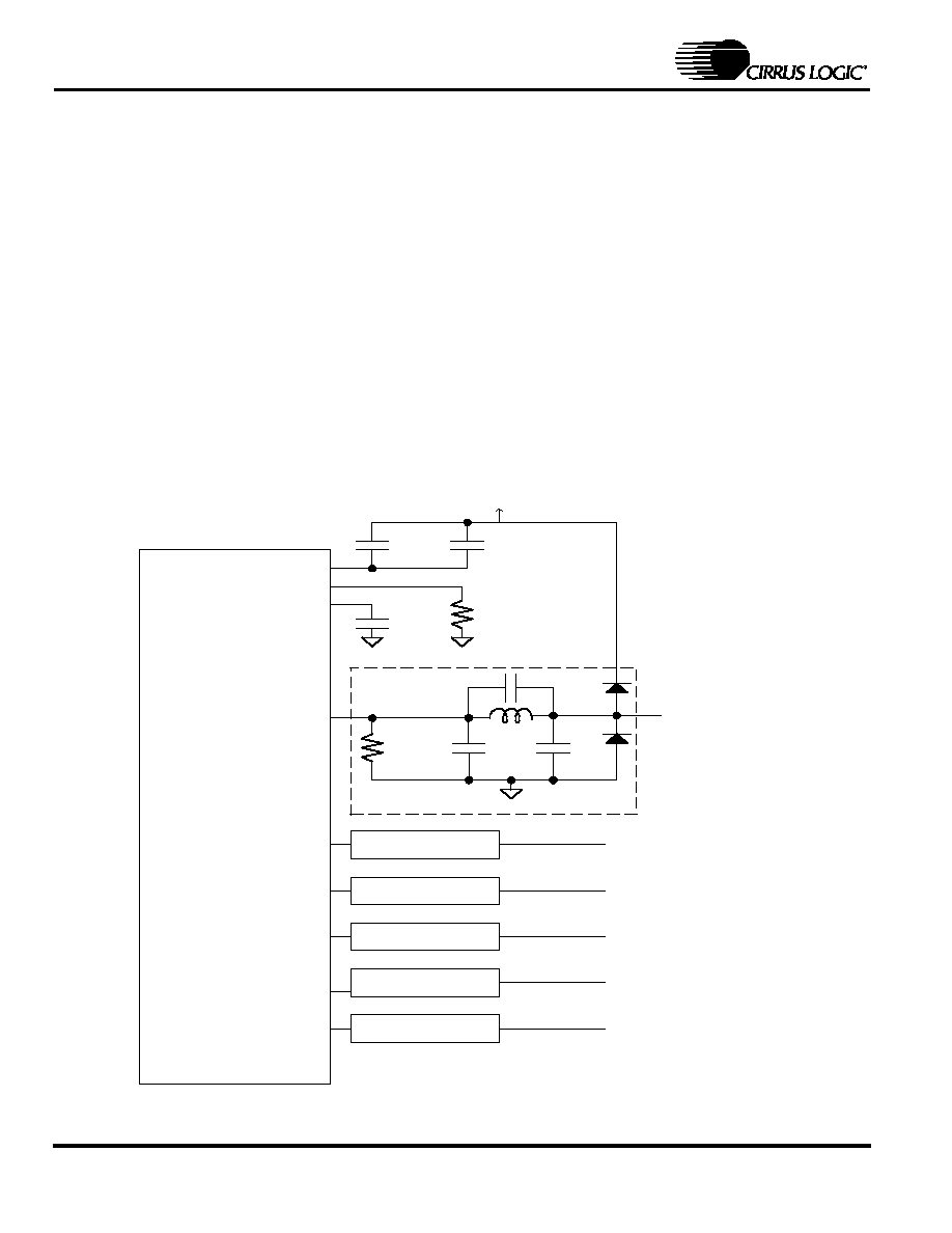
5.10
Video Encoder with Progressive Video
DACs
The CS98200 incorporates an enhanced video
encoder with six 10-bit video DACs that drive
double terminated 75
directly without exter-
nal buffering. These termination resistors
should be located as close as possible to the
CS98200. All analog video outputs should be
connected through filters to video connectors
(TV/Monitor). The video filters should be locat-
ed as close as possible to the video connectors.
Two schottky diodes should be connected to
each output in order to protect the CS98200
from surges caused by being connected and dis-
connected to the external devices.
Figure 21
shows the video DAC connections.
Six 10-bit DACs provide two channels for an S-
Video output port, one composite video output,
and three RGB or Y, Pb, Pr outputs. Video out-
put can be formatted to be compatible with
NTSC (M,J), PAL (B, D, G, H, I, M, 60), and 480P.
The video encoder is compliant with both Mac-
rovision 7.1 for the interlaced video (NTSC,
PAL) and 1.03 for the progressive scan (480p).
The video encoder also supports WSS (Wide-
Screen Signaling), CGMS (Copy Generation
Management System), and Closed Caption.
C S 9 8 2 0 0
C O M P 1 & 2
R S E T 1 & 2
V R E F 1 & 2
Y
C
C V
Y G
V R
U B
3 . 3 V
1 7 4
1 %
0 . 0 1 u F
0 . 0 1 u F
Y o u t
V i d o e F il t e r
V id e o F ilt e r
V id e o F ilt e r
V id e o F ilt e r
V id e o F ilt e r
V id e o F ilt e r
C o u t
C V o u t
V R o u t
Y G o u t
U B o u t
7 5
1 %
2 7 0 p F
3 3 0 p F
1 . 8 u H
2 2 p F
1 0 u F
Figure 21. Video DAC Connections

DS581PP2
Copyright 2002 Cirrus Logic (All Rights Reserved)
33
CS98200
Next Generation DVD Processor
5.11
Video Input/Output Interface
In addition to the six 10-bit video DACs, the
CS98200 provides a separate Digital Video In-
terface that will give you flexible and powerful
means of outputting digital video data to exter-
nal devices in CCIR601/3 and CCIR656 formats.
The interface directly supports NTSC/PAL vid-
eo encoding, in both master and slave synchro-
nization configurations. The internal frame
buffer format could be 4:2:0, 4:2:2, YUV655,
RGB565 and RGB555.
The CS98200 also features an NTSC/PAL video
decoder input interface. The interface accepts
CCIR601, CIF, and QCIF formats, out of many
TV decoders on the market. The video processor
also allows overlay of multiple video planes
(main video / video input / picture_in_picture
/ on-screen display).
The Video Input Scaler (VIS) module inputs 8-
bit digital video data from a camera or
PAL/NTSC decoder and simply dump all the
data to DRAM. The scaled image, with a border,
can be overlaid anywhere on the screen into a �
or �-screen sized window by the Picture in Pic-
ture (PIP) module.
An alternate method of using the Video Input
function is to input a full sized picture and
present it on the screen full size (bypass mode).
In this mode, the PIP module can place full mo-
tion DVD images in the small window. An inter-
nal glitch-free mux can switch the video
processor clock source from the internal clock to
the Video Input clock, allowing the PIP mode to
switch back and forth on the fly, with no drop-
out.

34
Copyright 2002 Cirrus Logic (All Rights Reserved)
DS581PP2
CS98200
Next Generation DVD Processor
5.12
Universal Asynchronous
Receiver/Transmitters (UARTs)
The UART performs serial-to-parallel conver-
sion on data characters received from a periph-
eral device and parallel-to-serial conversion on
data characters received from the host proces-
sor.
Figure 22
shows RXD and TXD data trans-
fers over the UART interface.
The CS98200 has 2 UART interfaces based on a
NS16550-compatible design, which incorpo-
rates 16-byte transmit and receive FIFOs to en-
hance performance and throughput. As with
the 16650, it can operate in both FIFO-mode
(16550) or in the original non-FIFO mode
(16450). The main registers are identical in
structure to the NS16550, but some unused bits
have been enabled for added functionality.
The standard features are:
� Compatible with 16450 UART
� 16-byte transmit and receive FIFOs reduce
number of interrupts presented to CPU
� Generates and detects standard asynchronous
communication bits (start, stop and parity) to
and from serial data
� Independently controlled transmit, receive, line
status and data set interrupts
� Programmable baud rate generator (16 bit
divisor)
� Modem control interface (CTS, RTS, DSR, DTR,
RI and DCD)
� Fully programmable serial-interface
characteristics:
-- 5, 6, 7 or 8 bit characters
-- Even, odd or no-parity bit
generation/detection
-- 1, 1�, or 2 stop bit generation
� False start bit detection
� Complete status reporting capabilities
� Line break generation and detection
� Internal loopback diagnostic mode
� Programmable trigger levels for FIFOs
� Selectable DMA signaling mode
� Prioritized interrupts
� Transmitter and receiver FIFO time-out
interrupts
Additional optimizations:
� Byte enable register allows transfer of up to 4
bytes in a single register write (only in FIFO
mode).
� External loopback diagnostic mode
� Separate baud clock input available
� Additional receiver error information
Note: If using separate baud clock, it must be less
than � frequency of the system clock,
otherwise, you must use the system clock.
R X D
T X D
P a rity
D a ta B its (5 ~ 8 )
S ta rt
S to p
P a rity
D a ta B its (5 ~ 8 )
S ta rt
S to p
S ta rt
Figure 22. UART Data Transfer
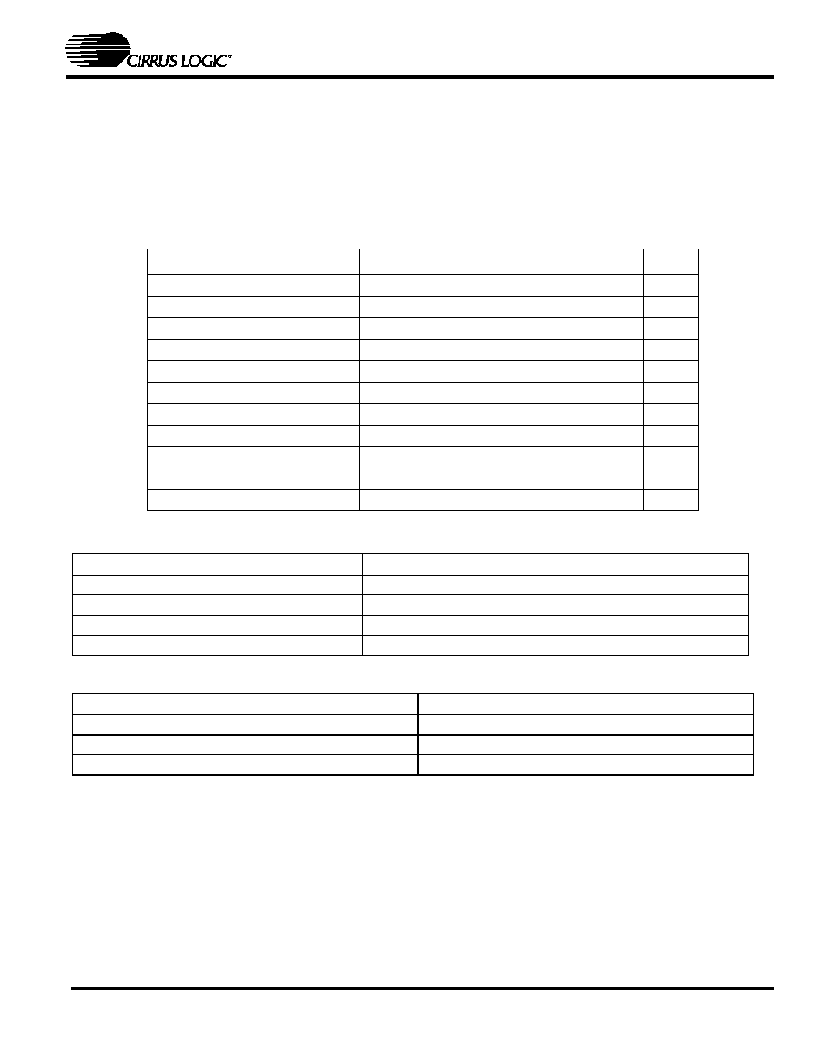
DS581PP2
Copyright 2002 Cirrus Logic (All Rights Reserved)
35
CS98200
Next Generation DVD Processor
6. MEMORY MAP
6.1
Processor Memory Map
The CS98200 externally supports up to 32 Mbytes DRAM and 16 Mbytes ROM/NVRAM.
Table 9
,
Table 10,
and
Table 11
on the next page list the memory map as viewed by the RISC processors, and
identifies whether each segment is mapped or cacheable.
For detailed information on programming CS98200 memory, see
CS98200 Memory Interface User's
Manual (DS525UMD1).
Address
Description
Cached
0x8000_0000 - 0x8000_7FFF
Internal SRAM (32 Kbytes)
Yes
0x8200_0000 - 0x83FF_FFFF
External DRAM (32 Mbytes)
Yes
0x9400_0000 - 0x97FF_FFFF
External DRAM w/ Dcache flush (32 Mbytes)
Yes
0x9800_0000 - 0x9BFF_FFFF
External ROM/NVRAM read/write (16 Mbytes)
Yes
0x9C00_0000 - 0x9FFF_FFFF
External ROM/NVRAM read only (16 Mbytes)
Yes
0xA000_0000 - 0xA000_7FFF
Internal SRAM (32 Kbytes)
No
0xA200_0000 - 0xA3FF_FFFF
External DRAM (32 Mbytes)
No
0xB000_0000 - 0xB003_FFFF
Internal registers and SRAMs
No
0xB400_0000 - 0xB7FF_FFFF
External DRAM w/ Dcache flush (32 Mbytes)
No
0xB800_0000 - 0xBBFF_FFFF
External ROM/NVRAM read/write (16 Mbytes)
No
0xBC00_0000 - 0xBFFF_FFFF
External ROM/NVRAM read only (16 Mbytes)
No
Table 9. Memory Map-RISC0 Processor
Host Byte Address
Description
0x0000_0000 - 0x0003_FFFF
Internal registers and SRAMs
0x1000_0000 - 0x11FF_FFFF
External DRAM (32 Mbytes)
0x1200_0000 - 0x13FF_FFF
Internal SRAM
0x1400_0000 - 0x14FF_FFFF
External ROM/NVRAM space (16 Mbytes)
Table 10. Host Debug Port Address Map
Byte Address Offset
Description
0x0000_0000 - 0x0003_FFFF (I/O space)
Internal Registers and SRAMs
0x0000_0000 - 0x01FF_FFFF (memory space)
External DRAM (32 Mbytes)
0x0200_0000 - 0x0200_7FFF (memory space)
Internal SRAM (32 Kbytes)
Table 11. DSP Address Map
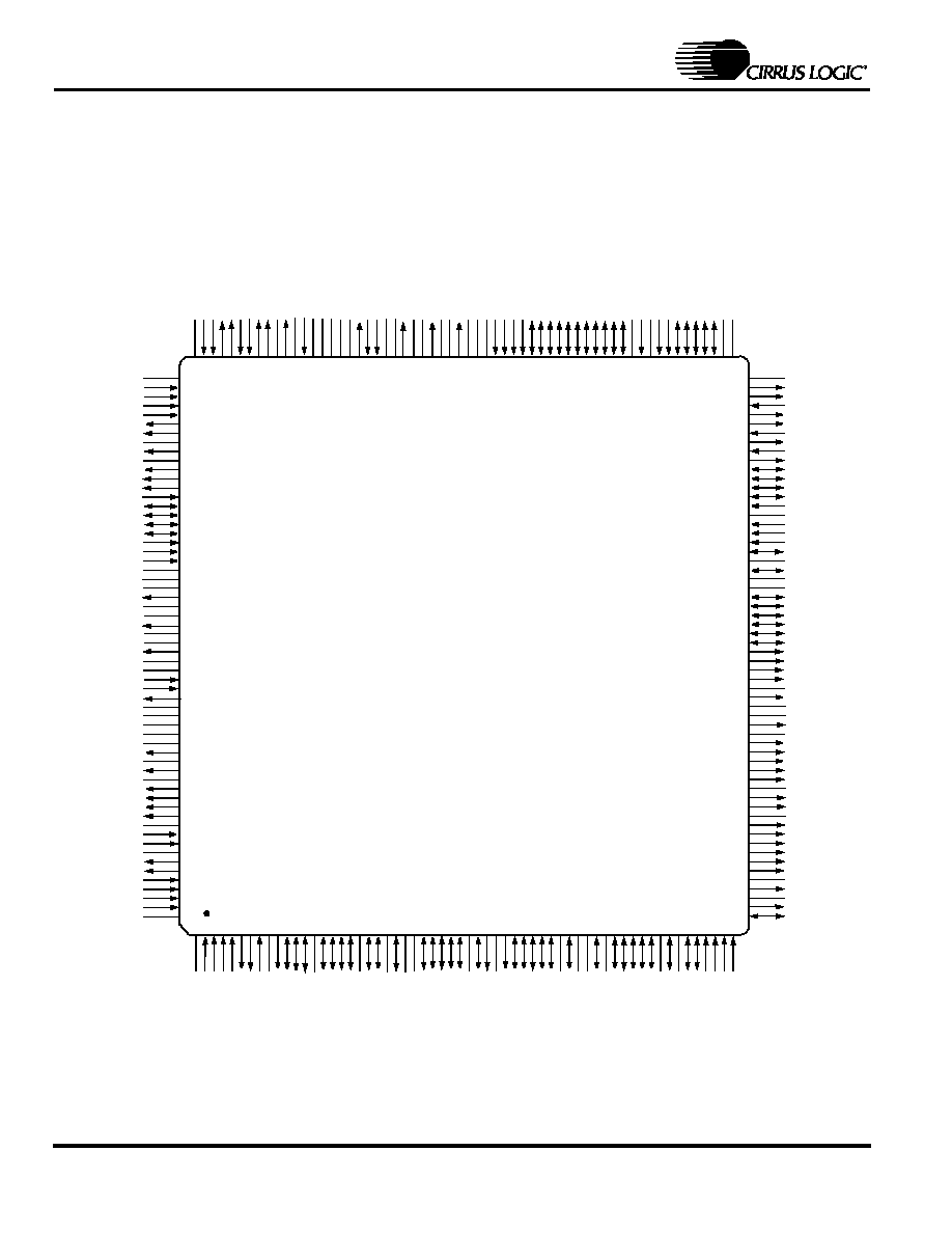
36
Copyright 2002 Cirrus Logic (All Rights Reserved)
DS581PP2
CS98200
Next Generation DVD Processor
7. 240-PIN MQFP PIN DESCRIPTION
7.1
240-Pin MQFP Pin Layout
Figure 23
shows the layout of all the pins for the 240-pin MQFP package. The direction of the arrow
by each pin shows whether the pin is an input, output, or bidirectional.
CS98200
240-Pin MQFP
2
3
4
5
6
7
8
9
10
11
12
13
14
15
16
17
18
19
20
21
22
23
24
25
26
27
28
29
30
31
32
33
34
35
36
37
38
39
40
41
42
43
44
45
46
47
48
49
51
50
52
1
IR
_
I
N
CD
C_
CL
K
CDC_
SYNC
CD
C_
S
D
O
CDC
_
S
DI
M
_
D
_29
IO
_
G
N
D
M
_
D
_28
M
_
D
_27
M
_
D
_26
M
_
D
_25
I
O
_3V
3
M
_
D
_30
M
_
D
_31
M
_
D
_23
D
I
G
_1V
8
D
I
G
_1V
8
DI
G
_
GN
D
DI
G
_
GN
D
IO
_
G
N
D
M
_
D
_21
M
_
D
_20
M
_
D
_19
M
_
D
_18
M
_
D
_17
I
O
_3V
3
I
O
_3V
3
IO
_
G
N
D
M_
D
Q
M_
1
M_
D
Q
M_
3
M
_
D
_14
M
_
D
_13
M_
D
_
6
M_
D
_
5
M_
D
Q
M_
2
M
_
D
_22
RST
_
N
TEST
P
LL_1V
8
M
_
D
_24
M
_
D
_16
M
_
D
_15
M
_
D
_12
M
_
D
_11
I
O
_3V
3
M
_
D
_10
IO
_
G
N
D
M_
D
_
9
M_
D
_
8
IO
_
G
N
D
M_
D
_
7
M_
D
_
4
53
54
55
57
56
58
59
60
M_
D
_
3
VI
N_
D_
1
VI
N_
D_
0
I
O
_3V
3
M_
D
_
2
VI
N_
D_
3
M_
D
_
1
VI
N_
D_
2
119
118
117
116
115
114
113
112
111
110
109
108
107
106
105
104
103
102
101
100
99
98
97
96
95
94
93
92
91
90
89
88
87
86
85
84
83
82
81
80
79
78
77
76
75
74
73
72
70
71
69
120
68
67
66
64
65
63
62
61
DV DL_DI
DV D_RDY
PW M_O
RX D_2
TXD _2
SD A1
SC L1
VIN_D_7
IO_3V3
VIN_D_6
VIN_D_5
VIN_D_4
SC L2
SD A2
DIG_1V8
NV _D_6
IO_3V3
M _A_9
IO_GN D
NV _D_5
NV _D_4
NV _D_3
NV _D_2
NV _D_1
NV _D_0
M _A_0
RX D_1
M _A_3
IO_3V3
TXD _1
IO_GN D
DIG_G ND
IO_GN D
M _CAS_N
M _A_2
DIG_G ND
DV DL_CK
DV DL_DO
PLL_1V8
NV _D_7
M _A_1
M _A_4
M _A_5
DIG_1V8
M _A_6
M _A_7
M _A_8
M _A_10
NV _CE_N
M _BS0_N
M _W E_N
M _RAS_N
M _BS1_N
IO_GN D
M _CKO
M _AP
M _CKE
M _D_0
IO_3V3
M _DQM _0
17
9
17
8
17
7
17
6
17
5
17
4
17
3
17
2
17
1
17
0
16
9
16
8
16
7
16
6
16
5
16
4
16
3
16
2
16
1
16
0
15
9
15
8
15
7
15
6
15
5
15
4
15
3
15
2
15
1
15
0
14
9
14
8
14
7
14
6
14
5
14
4
14
3
14
2
14
1
14
0
13
9
13
8
13
7
13
6
13
5
13
4
133
13
2
130
13
1
12
9
18
0
128
12
7
12
6
124
12
5
12
3
122
121
H_
A
L
E
H_
A
_
3
DVD_
D_
1
DV
D_
D
_
0
H_
A
_
2
D
V
DL
_
RDY
D
A
C_
A3
V3
D
A
C_
A3
V3
DA
C
_
A
G
ND
D
A
C_
A3
V3
DA
C
_
A
G
ND
VR
E
F
1
DI
G
_
1
V
8
H_
A
_
0
CO
M
P
1
DA
C
_
A
G
ND
H_
D
_
7
H_
D
_
9
CV
_
O
U
T
DA
C
_
A
G
ND
D
A
C_
A3
V3
Y_
O
U
T
DA
C
_
A
G
ND
D
A
C_
A3
V3
C_
O
U
T
D
A
C_
DG
ND
H_
A
_
1
C
D
_C
2P
0
CD
_
D
A
T
A
DI
G
_
GN
D
CD
_
B
C
L
K
H
_
D
_15
IO
_
G
N
D
V
I
N_
CL
K
DA
C
_
A
G
ND
D
A
C_
A3
V3
D
V
D_
D_
3
D
V
D_
D_
2
PL
L
_
1
V8
I
SET1
D
A
C_
D1
V8
C
D
_
L
RCK
H
_
D
_14
H
_
D
_13
H
_
D
_12
H
_
D
_11
H
_
D
_10
H_
D
_
8
H_
D
_
6
V
I
N_
HS
H_
D
_
5
I
O
_3V
3
VI
N
_
V
S
H_
D
_
0
H_
D
_
1
H_
D
_
4
H_
D
_
3
PL
L
_
1
V8
H_
D
_
2
IO
_
G
N
D
182
183
184
185
186
187
188
189
190
191
192
193
194
195
196
197
198
199
200
201
202
203
204
205
206
207
208
209
210
211
212
213
214
215
216
217
218
219
220
221
222
223
224
225
226
227
228
229
231
230
232
181
233
234
235
237
236
238
239
240
DVD _D_6
DVD _D_7
H_CS_0
H_CS_1
IO _3V3
H_W R
H_RD Y
SPI_C LK
S PI_DO
SP I_DI
S PI_RD Y
A UDI_D
H_R D
H_C S_3
AU DI_BC K
DA C_AGN D
AUD_XC LK
AU DO_BC K
DA C_DGN D
UB_OU T
DAC _A3V3
DA C_AGN D
YG_OU T
DAC _A3V3
DA C_AGN D
VR_OU T
H_C S_2
COM P2
IS ET2
IO_GN D
DA C_AGN D
DAC _A3V3
AUDO _D_3
IO _3V3
DA C_AGN D
DAC_D 1V8
DVD _D_4
DVD _D_5
PLL_GN D
A UDI_LR
DAC _A3V3
VR EF2
DA C_AGN D
DAC _A3V3
DAC _A3V3
AUDO _LR
DIG _1V8
DIG_GN D
AUDO _D_1
XTLCLK_O
AUDO _D_2
XTLCLK_I
IO_GN D
DVD_SO S
DVD_EN A
AUDO _D_0
S PDIF_O
PLL_GN D
DVD_S TB
DVD_ER R
Figure 23. 240-Pin MQFP Pin Layout
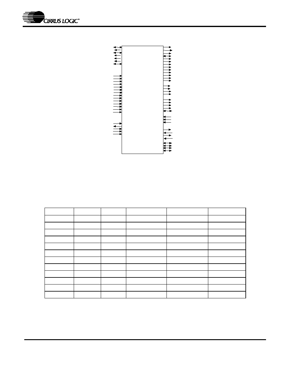
DS581PP2
Copyright 2002 Cirrus Logic (All Rights Reserved)
37
CS98200
Next Generation DVD Processor
7.2
240-Pin MQFP Pin Summary
Figure 24
shows the pin names associated with each type of CS98200 interface.
7.3
Pin Configuration Summary
The CS98200 has flexible pin functionality.
Table 12
lists the different possible pin configurations
and the settings required. The IO_Set value is programmed through a register, while the
AUDO_D_0 and AUDO_LR values are set through pull up or pull down resistors on the pins.
IO_Set[1:0] AUDO_D_0 AUDO_LR Host/ATAPI Pins
Video In/Out Pins
DVD Pins
00
1
X
Host master mode Video in mode
DVD mode
00
0
0
Host slave mode
Video in mode
DVD mode
00
0
1
Host master mode Video in mode
Host slave mode
01
1
X
Host master mode Video out mode
Video in mode
01
0
0
Host slave mode
Video out mode
Video in mode
01
0
1
Host master mode Video out mode
Host slave mode
10
1
X
DVD mode
Video in mode
GPIO mode
10
0
0
Host slave mode
Video in mode
GPIO mode
10
0
1
DVD mode
Video in mode
Host slave mode
11
1
X
DVD mode
Video out mode
Video in mode
11
0
0
Host slave mode
Video out mode
Video in mode
11
0
1
DVD mode
Video out mode
Host slave mode
Table 12. Pin Configuration Summary
Figure 24. 240-Pin MQFP Pinout Summary
H _ D _ [ 1 5 : 0 ]
H _ C S _ [ 3 : 0 ]
H _ A _ [ 3 : 0 ]
H _ A L E
H _ R D
H _ W R
H _ R D Y
D V D _ D [ 7 : 0 ]
D V D L _ R D Y
D V D _ S T B
D V D _ E N A
M _ A _ [ 1 0 : 0 ]
M _ B S 0 _ N
M _ D _ [ 3 1 : 0 ]
M _ D Q M _ [ 3 : 0 ]
M _ R A S _ N
M _ C A S _ N
M _ A P
M _ C K E
M _ C K O
M _ W E _ N
N V _ C E _ N
V I N _ H S / V O U T _ H S
V I N _ V S / V O U T _ V S
V I N _ C L K / V O U T _ C L K
V I N _ D [ 7 : 0 ] / V O U T _ D [ 7 : 0 ]
A U D I _ B C K
A U D I _ L R
A U D I _ D _ [ 3 : 0 ]
A U D O _ B C K
A U D O _ L R
A U D O _ D _ [ 3 : 0 ]
I R _ I N
T E S T
X T L C L O C K _ I
R S T _ N
C S 9 8 2 0 0
H o s t M a s t e r / A T A P I
( 2 8 )
M e m o r y
I n t e r f a c e
( 6 4 )
V i d e o I n / O u t
( 1 1 )
A u d i o O u t
( 8 )
M i s c .
( 5 )
A u d i o I n p u t
( 5 )
S P D I F _ O
D V D L o a d e r I n t e r f a c e ( 2 0 )
U A R T s ( 4 )
P o w e r / G n d : ( 6 8 )
M _ B S 1 _ N
N V _ D [ 7 : 0 ]
A U D _ X C L K
R X D _ 1
T X D _ 1
R X D _ 2
T X D _ 2
I
2
C D e b u g ( 4 )
S C L 1
S D A 1
S C L 2
S D A 2
X T L C L O C K _ O
D V D _ S O S
D V D _ E R R
D V D _ R D Y
D V D L _ D I
D V D L _ D O
D V D L _ C K
C D _ B C L K
C D _ L R C K
C D _ D A T A
C D _ C 2 P O
38
Copyright 2002 Cirrus Logic (All Rights Reserved)
DS581PP2
CS98200
Next Generation DVD Processor
7.4
Explanation of Pin Types
Table 13
lists the conventions used to identify the pin type and direction.
7.5
240-Pin MQFP Pin Assignments
Table 14
lists the pin number, pin name, and pin type for the 240-pin CS98200 package. The primary
function and pin direction is shown for all signal pins. For some signal pins, a secondary function
(or functions) and direction are also shown. For pins having more than one function, the primary
function is chosen when the chip is reset.
Pin Type
Direction
I
Input
IS
Input, with schmitt trigger
ID
Input, with pull down resistor
IU
Input, with pull up resistor
O
Output
O4
Output � 4 mA drive
O8
Output � 8 mA drive
T4
High-Z Output � 4mA drive
B
Bi-direction
B4
Bi-direction � 4 mA drive
B4U
Bi-direction � 4 mA drive, with pull-up
B8U
Bi-direction � 8 mA drive, with pull-up
B4S
Bi-direction � 4 mA drive, with Schmitt trigger
B4SU
Bi-direction � 4 mA drive, with pull-up and Schmitt trigger
Pwr
+1.8 V or +3.3 V power supply voltage
Gnd
Power supply ground
Name_N
Low active
Table 13. Pin Type Legen d
Pin #
Pin Name
Type
Primary Function
Dir
Secondary Function(s)
Dir
1
PLL_1V8
Pwr
PLL Power 1.8 V
2
RST_N
ISU
Reset
I
3
TEST
I
Manufacturing Test
I
4
IR_IN
ISU
IR in
I
5
CDC_CLK
B4S
GPIO_MIS[18]
B
6
CDC_SYNC
B4S
GPIO_MIS[19]
B
7
CDC_SDO
B4S
GPIO_MIS[20]
B
8
CDC_SDI
B4S
GPIO_MIS[21]
B
9
IO_3V3
Pwr
IO Power 3.3 V
10
M_DQM_3
B8
DRAM Byte_Enable[3]
O
Table 14. 240-Pin MQFP Pin Assignments
DS581PP2
Copyright 2002 Cirrus Logic (All Rights Reserved)
39
CS98200
Next Generation DVD Processor
11
M_D_31
B8
DRAM Data[31]
B
12
M_D_30
B8
DRAM Data[30]
B
13
M_D_29
B8
DRAM Data[29]
B
14
IO_GND
Gnd
IO Ground
15
M_D_28
B8
DRAM Data[28]
B
NVRAM Address[23]
O
16
M_D_27
B8
DRAM Data[27]
B
NVRAM Address[22]
O
17
M_D_26
B8
DRAM Data[26]
B
NVRAM Address[21]
O
18
M_D_25
B8
DRAM Data[25]
B
NVRAM Address[20]
O
19
IO_3V3
Pwr
IO Power 3.3 V
20
M_D_24
B8
DRAM Data[24]
B
NVRAM Address[19]
O
21
M_D_23
B8
DRAM Data[23]
B
NVRAM Address[18]
O
22
DIG_1V8
Pwr
Digital Power 1.8 V
23
M_D_22
B8
DRAM Data[22]
B
NVRAM Address[17]
O
24
DIG_GND
Gnd
Digital Ground
25
IO_GND
Gnd
IO Ground
26
M_D_21
B8
DRAM Data[21]
B
NVRAM Address[16]
O
27
M_D_20
B8
DRAM Data[20]
B
NVRAM Address[15]
O
28
M_D_19
B8
DRAM Data[19]
B
NVRAM Address[14]
O
29
M_D_18
B8
DRAM Data[18]
B
NVRAM Address[13]
O
30
M_D_17
B8
DRAM Data[17]
B
NVRAM Address[12]
O
31
IO_3V3
Pwr
IO Power 3.3 V
32
M_D_16
B8
DRAM Data[16]
B
NVRAM Address[11]
O
33
M_DQM_2
B8
DRAM Byte_Enable[2]
O
34
IO_GND
Gnd
IO Ground
35
M_DQM_1
B8
DRAM Byte_Enable[1]
O
36
M_D_15
B8
DRAM Data[15]
B
37
M_D_14
B8
DRAM Data[14]
B
38
M_D_13
B8
DRAM Data[13]
B
39
M_D_12
B8
DRAM Data[12]
B
40
M_D_11
B8
DRAM Data[11]
B
41
IO_3V3
Pwr
IO Power 3.3 V
Pin #
Pin Name
Type
Primary Function
Dir
Secondary Function(s)
Dir
Table 14. 240-Pin MQFP Pin Assignments (Continued)

40
Copyright 2002 Cirrus Logic (All Rights Reserved)
DS581PP2
CS98200
Next Generation DVD Processor
42
M_D_10
B8
DRAM Data[10]
B
43
IO_GND
Gnd
IO Ground
44
DIG_GND
Gnd
Digital Ground
45
M_D_9
B8
DRAM Data[9]
B
46
DIG_1V8
Pwr
Digital Power 1.8 V
47
M_D_8
B8
DRAM Data[8]
B
48
M_D_7
B8
DRAM Data[7]
B
49
M_D_6
B8
DRAM Data[6]
B
50
M_D_5
B8
DRAM Data[5]
B
51
M_D_4
B8
DRAM Data[4]
B
52
IO_GND
Gnd
IO Ground
53
M_D_3
B8
DRAM Data[3]
B
54
IO_3V3
Pwr
IO Power 3.3 V
55
M_D_2
B8
DRAM Data[2]
B
56
M_D_1
B8
DRAM Data[1]
B
57
VIN_D_0
B4
Primary Video_In Data[0]
I
(1.) Secondary Video_Out Data[0]
(2.) GPIO_VIS[0]
O
B
58
VIN_D_1
B4
Primary Video_In Data[1]
I
(1.) Secondary Video_Out Data[1]
(2.) GPIO_VIS[1]
O
B
59
VIN_D_2
B4
Primary Video_In Data[2]
I
(1.) Secondary Video_Out Data[2]
(2.) GPIO_VIS[2]
O
B
60
VIN_D_3
B4
Primary Video_In Data[3]
I
(1.) Secondary Video_Out Data[3]
(2.) GPIO_VIS[3]
O
B
61
M_D_0
B8
DRAM Data[0]
B
62
M_DQM_0
B8
DRAM Byte_En[0]
O
63
IO_GND
Gnd
IO Ground
64
M_CKO
O8
DRAM Clock
O
Drc_Clock Eternal Input
I
65
IO_3V3
Pwr
IO Power 3.3 V
66
M_CKE
B8
DRAM Clock Enable
O
67
M_AP
B8
DRAM Auto Precharge
O
NVRAM_OE_N
O
68
M_BS1_N
B8
DRAM BankSel[1]
O
69
M_BS0_N
B8
DRAM BankSel[0]
O
70
M_RAS_N
B8
DRAM Row Strobe
O
Pin #
Pin Name
Type
Primary Function
Dir
Secondary Function(s)
Dir
Table 14. 240-Pin MQFP Pin Assignments (Continued)

DS581PP2
Copyright 2002 Cirrus Logic (All Rights Reserved)
41
CS98200
Next Generation DVD Processor
71
M_CAS_N
B8
DRAM Col. Strobe
O
72
IO_GND
Gnd
IO Ground
73
M_WE_N
B8
DRAM Write Enable
O
NVRAM_WE_N
O
74
NV_CE_N
O4
ROM Chip Enable
O
75
IO_3V3
Pwr
IO Power 3.3 V
76
M_A_10
B8
DRAM Address[10]
O
NVRAM Address[10]
O
77
M_A_9
B8
DRAM Address[9]
O
NVRAM Address[9]
O
78
M_A_8
B8
DRAM Address[8]
O
NVRAM Address[8]
O
79
M_A_7
B8
DRAM Address[7]
O
NVRAM Address[7]
O
80
M_A_6
B8
DRAM Address[6]
O
NVRAM Address[6]
O
81
DIG_1V8
Pwr
Digital Power 1.8 V
82
M_A_5
B8
DRAM Address[5]
O
NVRAM Address[5]
O
83
DIG_GND
Gnd
Digital Ground
84
IO_GND
Gnd
IO Ground
85
M_A_4
B8
DRAM Address[4]
O
NVRAM Address[4]
O
86
IO_3V3
Pwr
IO Power 3.3 V
87
M_A_3
B8
DRAM Address[3]
O
NVRAM Address[3]
O
88
M_A_2
B8
DRAM Address[2]
O
NVRAM Address[2]
O
89
M_A_1
B8
DRAM Address[1]
O
NVRAM Address[1]
O
90
M_A_0
B8
DRAM Address[0]
O
NVRAM Address[0]
O
91
NV_D_0
B8
NVRAM Data[0]
B
92
NV_D_1
B8
NVRAM Data[1]
B
93
NV_D_2
B8
NVRAM Data[2]
B
94
NV_D_3
B8
NVRAM Data[3]
B
95
NV_D_4
B8
NVRAM Data[4]
B
96
NV_D_5
B8
NVRAM Data[5]
B
97
IO_GND
Gnd
IO Ground
98
DIG_GND
Gnd
Digital Ground
99
NV_D_6
B8
NVRAM Data[6]
100
DIG_1V8
Pwr
Digital Power 1.8 V
101
NV_D_7
B8
NVRAM Data[7]
Pin #
Pin Name
Type
Primary Function
Dir
Secondary Function(s)
Dir
Table 14. 240-Pin MQFP Pin Assignments (Continued)
42
Copyright 2002 Cirrus Logic (All Rights Reserved)
DS581PP2
CS98200
Next Generation DVD Processor
102
VIN_D_4
B4
Primary Video_In Data[4]
I
(1.) Secondary Video_Out Data[4]
(2.) GPIO_VIS[4]
O
B
103
VIN_D_5
B4
Primary Video_In Data[5]
I
(1.) Secondary Video_Out Data[5]
(2.) GPIO_VIS[5]
O
B
104
VIN_D_6
B4
Primary Video_In Data[6]
I
(1.) Secondary Video_Out Data[6]
(2.) GPIO_VIS[6]
O
B
105
IO_3V3
Pwr
IO Power 3.3 V
106
VIN_D_7
B4
Primary Video_In Data[7]
I
(1.) Secondary Video_Out Data[7]
(2.) GPIO_VIS[7]
O
B
107
SCL1
B4SU
I
2
C Debug Slave
B
108
SDA1
B4SU
I
2
C Debug Slave
B
109
SCL2
B4SU
I
2
C Master/Simple Slave
B
GPIO_MIS[0]
B
110
SDA2
B4SU
I
2
C Master/Simple Slave
B
GPIO_MIS[1]
B
111
TXD_1
B4
UART1 Tx Data
O
GPIO_MIS[6]
B
112
RXD_1
B4
UART1 Rx Data
I
GPIO_MIS[7]
B
113
TXD_2
B4
UART2 Tx Data
O
GPIO_MIS[8]
B
114
RXD_2
B4
UART2 Rx Data
I
GPIO_MIS[9]
B
115
PWM_O
B4
PWM Output
O
GPIO_MIS[10]
B
116
DVD_RDY
B4
Prim. DVD Loader data Request
O
GPIO_DVD[12]
B
117
DVDL_DI
B4
Primary DVD Control Data In
I
(1.) Secondary Video_In Vsync
(2.) GPIO_DVD[13]
(3.) Secondary Host Slave Read
I
B
I
118
DVDL_DO
B4
Primary DVD Control Data Out
O
(1.) Secondary Video_In Hsync
(2.) GPIO_DVD[14]
(3.) Secondary Host Slave Write
I
B
I
119
DVDL_CK
B4S
Primary DVD Control Clock
O
(1.) Secondary Video_In Clock
(2.) GPIO_DVD[15]
(3.) Secondary Host Slave Ready
I
B
O
120
PLL_1V8
Pwr
PLL Power 1.8 V
121
PLL_GND
Gnd
PLL Ground
122
IO_GND
Gnd
IO Ground
123
H_D_0
B4
Host Master Data[0]
B
(1.) Secondary DVD Data[0]
(2.) GPIO_HST[0]
(3.) Primary Host Slave Data[0]
(4.) Primary Video_Out Data[0]
I
B
B
O
Pin #
Pin Name
Type
Primary Function
Dir
Secondary Function(s)
Dir
Table 14. 240-Pin MQFP Pin Assignments (Continued)
DS581PP2
Copyright 2002 Cirrus Logic (All Rights Reserved)
43
CS98200
Next Generation DVD Processor
124
H_D_1
B4
Host Master Data[1]
B
(1.) Secondary DVD Data[1]
(2.) GPIO_HST[1]
(3.) Primary Host Slave Data[1]
(4.) Primary Video_Out Data[1]
I
B
B
O
125
H_D_2
B4
Host Master Data[2]
B
(1.) Secondary DVD Data[2]
(2.) GPIO_HST[2]
(3.) Primary Host Slave Data[2]
(4.) Primary Video_Out Data[2]
I
B
B
O
126
H_D_3
B4
Host Master Data[3]
B
(1.) Secondary DVD Data[3]
(2.) GPIO_HST[3]
(3.) Primary Host Slave Data[3]
(4.) Primary Video_Out Data[3]
I
B
B
O
127
H_D_4
B4
Host Master Data[4]
B
(1.) Secondary DVD Data[4]
(2.) GPIO_HST[4]
(3.) Primary Host Slave Data[4]
(4.) Primary Video_Out Data[4]
I
B
B
O
128
VIN_VS
B4
Primary Video_In Vsync
I
(1.) Secondary Video_Out Vsync
(2.) GPIO_VIS[8]
(3.) Host Master Chip Select[4]
O
B
O
129
VIN_HS
B4
Primary Video_In Hsync
I
(1.) Secondary Video_Out Hsync
(2.) GPIO_VIS[9]
(3.) Host Master Chip Select[5]
O
B
O
130
IO_3V3
Pwr
IO Power 3.3 V
131
VIN_CLK
B4S
Primary Video_In Clock
I
(1.) Secondary Video_Out Clock
(2.) GPIO_VIS[10]
O
B
132
IO_GND
Gnd
IO Ground
133
H_D_5
B4
Host Master Data[5]
B
(1.) Secondary DVD Data[5]
(2.) GPIO_HST[5]
(3.) Primary Host Slave Data[5]
(4.) Primary Video_Out Data[5]
I
B
B
O
134
H_D_6
B4
Host Master Data[6]
B
(1.) Secondary DVD Data[6]
(2.) GPIO_HST[6]
(3.) Primary Host Slave Data[6]
(4.) Primary Video_Out Data[6]
I
B
B
O
135
H_D_7
B4
Host Master Data[7]
B
(1.) Secondary DVD Data[7]
(2.) GPIO_HST[7]
(3.) Primary Host Slave Data[7]
(4.) Primary Video_Out Data[7]
I
B
B
O
136
H_D_8
B4
Host Master Data[8]
B
(1.) Secondary DVD Control Clock
(2.) GPIO_HST[8]
O
B
137
H_D_9
B4
Host Master Data[9]
B
(1.) Secondary DVD Control Ready
(2.) GPIO_HST[9]
I
B
138
H_D_10
B4
Host Master Data[10]
B
(1.) Secondary DVD Control Data Out
(2.) GPIO_HST[10]
O
B
139
H_D_11
B4
Host Master Data[11]
B
(1.) Secondary DVD Control Data In
(2.) GPIO_HST[11]
I
B
Pin #
Pin Name
Type
Primary Function
Dir
Secondary Function(s)
Dir
Table 14. 240-Pin MQFP Pin Assignments (Continued)
44
Copyright 2002 Cirrus Logic (All Rights Reserved)
DS581PP2
CS98200
Next Generation DVD Processor
140
H_D_12
B4
Host Master Data[12]
B
(1.) Secondary CD C2P0
(2.) GPIO_HST[12]
(3.) Secondary DVDS_VLD
I
B
I
141
H_D_13
B4S
Host Master Data[13]
B
(1.) Secondary CD_BCLK
(2.) GPIO_HST[13]
(3.) Secondary DVDS_CLK
I
B
I
142
H_D_14
B4
Host Master Data[14]
B
(1.) Secondary CD_LRLK
(2.) GPIO_HST[14]
(3.) Secondary DVDS_SOS
I
B
I
143
H_D_15
B4
Host Master Data[15]
B
(1.) Secondary CD_Data
(2.) GPIO_HST[15]
(3.) Secondary DVDS_DATA
I
B
I
144
CD_BCLK
B4S
Primary CD Bit Clock
I
(1.) Primary DVDS_CLK
(2.) GPIO_DVD[17]
(3.) Secondary Host Slave Address[0]
I
B
I
145
CD_LRCK
B4
Primary CD L/R Clock
I
(1.) Primary DVDS_SOS
(2.) GPIO_DVD[18]
(3.) Secondary Host Slave Address[1]
I
B
I
146
CD_DATA
B4
Primary CD Data
I
(1.) Primary DVDS_DATA
(2.) GPIO_DVD[19]
(3.) Secondary Host Slave Address[2]
I
B
I
147
CD_C2P0
B4
Primary CD C2P0
I
(1.) Primary DVDS_VLD
(2.) GPIO_DVD[20]
(3.) Secondary Host Slave Address[3]
I
B
B
148
DAC_AGND
Gnd
Analog Ground
149
DAC_D1V8
Pwr
Digital Power 1.8 V
150
DAC_DGND
Gnd
Digital Ground
151
C_OUT
Anlg
C_OUT
152
DAC_A3V3
Pwr
Analog Power 3.3 V
153
DAC_AGND
Gnd
Analog Ground
154
Y_OUT
Anlg
Y_OUT
155
DAC_A3V3
Pwr
Analog Power 3.3 V
156
DAC_AGND
Gnd
Analog Ground
157
CV_OUT
Anlg
CV_OUT
158
DAC_A3V3
Pwr
Analog Power 3.3 V
159
DAC_AGND
Gnd
Analog Ground
160
COMP1
Anlg
Compensation
161
ISET1
Anlg
Current Set
162
VREF1
Anlg
Voltage Ref
Pin #
Pin Name
Type
Primary Function
Dir
Secondary Function(s)
Dir
Table 14. 240-Pin MQFP Pin Assignments (Continued)
DS581PP2
Copyright 2002 Cirrus Logic (All Rights Reserved)
45
CS98200
Next Generation DVD Processor
163
DAC_AGND
Gnd
Analog Ground
164
DAC_A3V3
Pwr
Analog Power 3.3 V
165
DAC_AGND
Gnd
Analog Ground
166
DAC_A3V3
Pwr
Analog Power 3.3 V
167
DAC_A3V3
Pwr
Analog Power 3.3 V
168
DVDL_RDY
B4
Primary DVD Control Ready
I
(1.)GPIO_DVD[16]
(2.) Secondary Host Slave Chip_Select
B
I
169
DIG_1V8
Pwr
Digital Power 1.8 V
170
H_A_0
B4
Host Master Address[0]
O
(1.) GPIO_HST[16]
(2.) Primary Host Slave Address[0]
B
I
171
DIG_GND
Gnd
Digital Ground
172
H_A_1
B4
Host Master Address[1]
O
(1.) GPIO_HST[17]
(2.) Primary Host Slave Address[1]
B
I
173
H_A_2
B4
Host Master Address[2]
O
(1.) GPIO_HST[18]
(2.) Primary Host Slave Address[2]
B
I
174
DVD_D_0
B4
Primary DVD Data[0]
I
(1.) Secondary Video_In Data[0]
(2.) GPIO_DVD[0]
(3.) Secondary Host Slave Data[0]
I
B
B
175
DVD_D_1
B4
Primary DVD Data[1]
I
(1.) Secondary Video_In Data[1]
(2.) GPIO_DVD[1]
(3.) Secondary Host Slave Data[1]
I
B
B
176
H_A_3
B4
Host Master Address[3]
O
(1.) GPIO_HST[19]
(2.) Primary Host Slave Address[3]
B
I
177
H_ALE
B4
Host Master Address Latch
O
GPIO_HST[20]
B
178
DVD_D_2
B4
Primary DVD Data[2]
I
(1.) Secondary Video_In Data[2]
(2.) GPIO_DVD[2]
(3.) Secondary Host Slave Data[2]
I
B
B
179
DVD_D_3
B4
Primary DVD Data[3]
I
(1.) Secondary Video_In Data[3]
(2.) GPIO_DVD[3]
(3.) Secondary Host Slave Data[3]
I
B
B
180
PLL_1V8
Pwr
PLL Power 1.8 V
181
PLL_GND
Gnd
PLL Ground
182
DVD_D_4
B4
Primary DVD Data[4]
I
(1.) Secondary Video_In Data[4]
(2.) GPIO_DVD[4]
(3.) Secondary Host Slave Data[4]
I
B
B
183
DVD_D_5
B4
Primary DVD Data[5]
I
(1.) Secondary Video_In Data[5]
(2.) GPIO_DVD[5]
(3.) Secondary Host Slave Data[5]
I
B
B
Pin #
Pin Name
Type
Primary Function
Dir
Secondary Function(s)
Dir
Table 14. 240-Pin MQFP Pin Assignments (Continued)

46
Copyright 2002 Cirrus Logic (All Rights Reserved)
DS581PP2
CS98200
Next Generation DVD Processor
184
DVD_D_6
B4
Primary DVD Data[6]
I
(1.) Secondary Video_In Data[6]
(2.) GPIO_DVD[6]
(3.) Secondary Host Slave Data[6]
I
B
B
185
DVD_D_7
B4
Primary DVD Data[7]
I
(1.) Secondary Video_In Data[7]
(2.) GPIO_DVD[7]
(3.) Secondary Host Slave Data[7]
I
B
B
186
H_CS_0
B4
Host Master Chip_Select[0]
O
(1.) Secondary DVD Start Sector
(2.) GPIO_HST[21]
(3.) Primary Host Slave Chip Select
I
B
I
187
H_CS_1
B4
Host Master Chip_Select[1]
O
(1) Secondary DVD Error
(2.) GPIO_HST[22]
I
B
188
IO_3V3
Pwr
IO Power 3.3 V
189
H_CS_2
B4
Host Master Chip_Select[2]
O
GPIO_HST[23]
B
190
IO_GND
Gnd
IO Ground
191
H_CS_3
B4
Host Master Chip_Select[3]
O
GPIO_HST[24]
B
192
H_RD
B4
Host Master Read
O
(1.) Secondary DVD Ready
(2.) GPIO_HST[25]
(3.) Primary Host Slave Read
O
B
I
193
H_WR
B4
Host Master Write
O
(1.) Secondary DVD Data Enable
(2.) GPIO_HST[26]
(3.) Primary Host Slave Write
I
B
I
194
H_RDY
B4S
Host Master Ready
I
(1.) Secondary DVD Data Strobe
(2.) GPIO_HST[27]
(3.) Primary Host Slave Ready
I
B
O
195
SPI_CLK
B4S
SPI Clock
B
GPIO_MIS[2]
B
196
SPI_DO
B4
SPI Data Out/InOut
B
GPIO_MIS[3]
B
197
SPI_DI
B4
SPI Data In
I
GPIO_MIS[4]
B
198
SPI_RDY
B4
SPI Ready / Chip Select
B
GPIO_MIS[5]
O
199
AUDI_D
B4
PCM Input Data
I
GPIO_MIS[15]
B
200
AUDI_LR
B4
PCM LR Clock
I
GPIO_MIS[16]
B
201
AUDI_BCK
B4S
PCM Input Clock
I
(1.) Aud_Pll_Aux_FIN[0]
(2.) GPIO_MIS[17]
(3.) AudioOut_Mute
I
B
O
202
DAC_AGND
Gnd
Analog Ground
203
DAC_D1V8
Pwr
Digital Power 1.8 V
204
DAC_DGND
Gnd
Digital Ground
205
UB_OUT
Anlg
UB_OUT_1
206
DAC_A3V3
Pwr
Analog Power 3.3 V
Pin #
Pin Name
Type
Primary Function
Dir
Secondary Function(s)
Dir
Table 14. 240-Pin MQFP Pin Assignments (Continued)

DS581PP2
Copyright 2002 Cirrus Logic (All Rights Reserved)
47
CS98200
Next Generation DVD Processor
207
DAC_AGND
Gnd
Analog Ground
208
YG_OUT
Anlg
YG_OUT_1
209
DAC_A3V3
Pwr
Analog Power 3.3 V
210
DAC_AGND
Gnd
Analog Ground
211
VR_OUT
Anlg
VR_OUT_1
212
DAC_A3V3
Pwr
Analog Power 3.3 V
213
DAC_AGND
Gnd
Analog Ground
214
COMP2
Anlg
Compensation
215
ISET2
Anlg
Current Set
216
VREF2
Anlg
Voltage Ref
217
DAC_AGND
Gnd
Analog Ground
218
DAC_A3V3
Pwr
Analog Power 3.3 V
219
DAC_AGND
Gnd
Analog Ground
220
DAC_A3V3
Pwr
Analog Power 3.3 V
221
DAC_A3V3
Pwr
Analog Power 3.3 V
222
AUDO_LR
B4
PCM LR Clock
O
(1.) Clock_Monitor_CPU
(2.) Host ParSlave_Set
O
I
223
DIG_1V8
Pwr
Digital Power 1.8 V
224
AUDO_BCK
B4
PCMO BCLK
O
(1.) Clock_Monitor_DRC
(2.) GPIO_MIS[11]
O
B
225
DIG_GND
Gnd
Digital Ground
226
AUD_XCLK
B4S
PCM MCLK Output
O
PCM MCLK External Input
I
227
AUDO_D_1
B4
PCM Data Out[1]
O
(1.) System Clock External Input
(2.) GPIO_MIS[12]
I
B
228
AUDO_D_2
B4
PCM Data Out[2]
O
(1.) CPU clock External Input
(2.) GPIO_MIS[13]
I
B
229
AUDO_D_3
B4
PCM Data Out[3]
O
(1.) Aud_PLL_AUX_FIN[1]
(2.) GPIO_MIS[14]
I
B
230
IO_3V3
Pwr
IO Power 3.3 V
231
XTLCLK_I
OSC
27 MHz Clock In
I
232
XTLCLK_O
OSC
27 MHz Clock Out
O
233
IO_GND
Gnd
IO Ground
234
AUDO_D_0
B4
PCM Data Out[0]
O
(1.) Main_Clock_Monitor
(2.) HostSlave_Par_I2C_Sel
O
I
Pin #
Pin Name
Type
Primary Function
Dir
Secondary Function(s)
Dir
Table 14. 240-Pin MQFP Pin Assignments (Continued)
48
Copyright 2002 Cirrus Logic (All Rights Reserved)
DS581PP2
CS98200
Next Generation DVD Processor
235
SPDIF_O
B4
SPDIF
O
Process_Monitor_Out
O
236
DVD_STB
B4S
Primary DVD Data Strobe
I
(1.) Host Master Address[4]
(2.) GPIO_DVD[8]
O
B
237
DVD_ENA
B4
Primary DVD Data Enable
I
(1.) Host Master Address[5]
(2.) GPIO_DVD[9]
O
B
238
DVD_SOS
B4
Primary DVD Start Sector
I
(1.) Host Master Address[6]
(2.) GPIO_DVD[10]
O
B
239
DVD_ERR
B4
Primary DVD Error
I
(1.) Host Master Address[7]
(2.) GPIO_DVD[11]
O
B
240
PLL_GND
Gnd
PLL Ground
Pin #
Pin Name
Type
Primary Function
Dir
Secondary Function(s)
Dir
Table 14. 240-Pin MQFP Pin Assignments (Continued)
DS581PP2
Copyright 2002 Cirrus Logic (All Rights Reserved)
49
CS98200
Next Generation DVD Processor
8. INTERFACE DESCRIPTIONS
8.1
SDRAM Interface Pins
These pins are used to interface the CS98200 with some external SDRAM. The CS98200 can interface
with SDRAM of various sizes. Only 32-bit data width is supported. Follow the instructions in
Table
15
on how to interface with any particular configuration of SDRAM.
8.2
ROM/NVRAM Interface Pins
This is the interface to the non-volatile memory that contains the firmware. See
Table 16
. It could be
either ROM, NVRAM � FLASH, or EEPROM, or any combination of these types of memory. This
interface can also connect to SRAM that would emulate a ROM on a development system. The bus
width is 8 bits.
Pin
Signal Name
Type
Description
11,12,13,15,16,
17,18,20,21,23,
26,27,28,29,30,
32,61, 56, 55,
53, 51, 50, 49,
48, 47, 45, 42,
40, 39, 38, 37,
36,
M_D[31:0]
B
Memory Data Bus. CS98200 uses all 32 bits.
90, 89, 88, 87,
85, 82, 80, 79,
78, 77, 76
M_A[10:0]
O
Memory Address Bus. Connect in order starting with M_A[0] to
all RAM address pins not already connected to M_BS[1:0]_N
or M_AP.
64
M_CKO
O
Memory Clock
66
M_CKE
O
Memory Clock Enable
69
M_BS0_N
O
Bank Selection. Always connect to RAM BS or BS0 pin.
68
M_BS1_N
O
Bank Selection. Always connect to RAM BS or BS0 pin.
67
M_AP
O
Memory Auto Pre-charge. Always connect to RAM AP pin.
70
M_RAS_N
O
Memory Row Address Strobe
71
M_CAS_N
O
Memory Column Address Strobe
73
M_WE_N
O
Memory Write Enable
62, 35, 33, 10
M_DQM[3:0]
O
IO Mask of Data Bus M_DQM[3] -> M_D[31:24]
Table 15. SDRAM Interface Pins
Pin
Signal Name
Type
Description
91,92,93,94,95,
96,99,101
NV_D[7:0]
B
Memory Data Bus.
90, 89, 88, 87,
85, 82, 80, 79,
78, 77, 76
M_A[10:0]
O
Memory Address Bus[10:0]
32, 30, 29, 28,
27, 26, 23, 21,
20, 18, 17, 16
M_D[31:16]
O
Memory Address Bus[23:11]
67
M_AP
O
Output Enable
73
M_WE_N
O
Write Enable.
Table 16. ROM/NVRAM Interfa c e

50
Copyright 2002 Cirrus Logic (All Rights Reserved)
DS581PP2
CS98200
Next Generation DVD Processor
8.3
Video Output Interface Pins
This is the interface to a video encoder chip that will send the CS98200 video signals to a TV. See
Table 17
. This interface uses the same pins of the Video Input Interface, so you are not able to use
Video Input (primary) and Video Output (Secondary) at the same time. .
8.4
Video Input Interface Pins
See
Table 18
.
74
NV_CE_N
O
ROM/NVRAM Chip Enable.
Pin
Signal Name
Type
Description
131s
VOUT_CLK
O
27 Mhz Clock Output.
129s
VOUT_HS
O
Horizontal Sync. Output when the CS98200 is the video
master, input when the video encoder is master.
128s
VOUT_VS
O
Vertical Sync. Output when the CS98200 is the video mas-
ter, input when the video encoder is master.
57s, 58s, 59s,
60s, 102s, 103s,
104s, 106s
VOUT_D[7:0]
O
Video Data Output[7:0] in Cb, Y, Cr, Y format.
Table 17. Video Output Interface
Pin
Signal Name
Type
Description
131
VIN_CLK
I
Video Input Clock.
128
VIN_VS
I
Video Input Vertical Sync.
129
VIN_HS
I
Video Input Horizontal Sync.
57, 58, 59, 60,
102, 103, 104,
106
VIN_D [7:0]
I
Video Data Input[7:0] in Cb, Y, Cr, Y format.
Table 18. Video Input Interface
Table 16. ROM/NVRAM Interface (Continued)
DS581PP2
Copyright 2002 Cirrus Logic (All Rights Reserved)
51
CS98200
Next Generation DVD Processor
8.5
Audio PCM Interface Pins
This is the audio PCM interface that connects to an audio CODEC. See
Table 19
. The sample rate and
the size of the samples are programmable for both input and output direction.
Pin
Signal Name
Type
Description
226
AUD_XCLK
B
Audio 256x/384x Clock input or output to Serial DAC. When
output, is generated from CS98200 internal PLL.
224
AUDO_BCK
O
Audio Bit Clock output to serial DAC.
222
AUDO_LR
O
Audio Out Left/Right Clock to serial DAC.
234
AUDO_D_0
O
Audio Serial Data Out[0].
227
AUDO_D_1
O
Audio Serial Data Out[1].
228
AUDO_D_2
O
Audio Serial Data Out[2].
229
AUDO_D_3
O
Audio Serial Data Out[3].
235
SPDIF_O
O
S/PDIF Output
201
AUDI_BCK
I
Audio Input Bit Clock. The CS98200 can be programmed to
use the Audio Output function's internally generated bit
clock, in which case this pin is not required.
200
AUDI_LR
I
Audio Input Left/Right Clock. The CS98200 can be pro-
grammed to use the Audio Output function's internally gen-
erated LR clock, in which case this pin is not required.
199
AUDI_D
I
Audio Input Data from Serial ADC.
Table 19. PCM Audio Interfa c e

52
Copyright 2002 Cirrus Logic (All Rights Reserved)
DS581PP2
CS98200
Next Generation DVD Processor
8.6
Host Master/ATAPI Interface
Pin
Signal Name
Type
Description
186, 187, 189,
191
H_CS[3:0]
O
Host Chip Select[3:0]. The host master can be pro-
grammed to use a different protocol for each of the 4
chip selects
177
H_ALE
O
Host address latch enable. Used for modes which
multiplex upper address information onto the data
lines
192
H_RD
O
Host Read Request.
193
H_WR
O
Host Write Request.
194
H_RDY
I
Host Ready. Connect to pull-up or pull-down if host
is not used.
170, 172, 173,
176
H_A[3:0]
O
Host Address[3:0].
123, 124, 125,
126, 127, 133,
134, 135, 136,
137, 138, 139,
140, 141, 142,
143
H_D[15:0]
B
Host Data Bus[15:0]. These pins can also output
Host Address during the address phase for multi-
plexed address/data mode. Tie together to pull-up
or pull-down if host is not used.
Table 20. Host Master/ATAPI Interface
DS581PP2
Copyright 2002 Cirrus Logic (All Rights Reserved)
53
CS98200
Next Generation DVD Processor
8.7
DVD Loader Interface
This interface connects to standard DVD loaders, and consists of three parts: Control, DVD Data and
CD Data. (See
Table 21
.) This interface shares CS98200 pins with the Host Master/ATAPI interface.
(See
Table 20 on page 52
.) The definition of the pins is set via register programming, and the two
modes are mutually exclusive.
8.8
DVD Serial Data Interface
This interface connects to the data port of low cost DVD loaders using a 4-wire serial interface. In this case,
control for the loader will typically be done using the 2-wire serial interface master. The ATAPI/IO channel
pins are then free to be used for a second DVD loader, a general purpose ATAPI, or as GPIOs.
Pin
Signal Name
Type
Description
174, 175, 178,
179, 182, 183,
184, 185
DVD_D[7:0]
I
Primary DVD Data
168
DVDL_RDY
I
Primary DVD Control Ready
236
DVD_STB
I
Primary DVD Data Strobe
237
DVD_ENA
I
Primary DVD Data Enable
238
DVD_SOS
I
Primary DVD Start Sector
239
DVD_ERR
I
Primary DVD Error
116
DVD_RDY
O
Primary DVD Data Request
117
DVDL_DI
I
Primary DVD Control Data In
118
DVDL_DO
O
Primary DVD Control Data Out
119
DVDL_CK
O
Primary DVD Control Clock
144
CD_BCLK
I
Primary CD Bit Clock
145
CD_LRCK
I
Primary CD L/R Clock
146
CD_DATA
I
Primary CD Data
147
CD_C2PO
I
Primary CD C2P0
Table 21. DVD I/O Channel Interface
Pin
Signal Name
Type
Description
144s /141s
DVDS_CLK
I
DVD Clock Input
146s/143s
DVDS_DATA
I
DVD serial data input (data can be input MSB or LSB first)
147s/140s
DVDS_VLD
I
DVD valid ( a bit of data is clocked in when this pin is high)
145s/142s
DVDS_SOS
I
DVD start of sector input
54
Copyright 2002 Cirrus Logic (All Rights Reserved)
DS581PP2
CS98200
Next Generation DVD Processor
8.9
SPI Interface
The SPI Interface supports industry standard 3-wire protocols. (See
Table 22
) In master mode, this
interface can control a front panel or a small non-volatile memory. In slave mode, it can operate un-
der control of an external processor, for example, in a combination unit.
8.10
General Purpose Input/Output (GPIO)
The CS98200 provides enough GPIO pins, each with individual output High-Z-state controls. High-
Z-state means that the output driver is turned off or placed in the high-impedance state.
Table 23
describes the General Purpose I/O Interface. Additional pins may also be re-defined as GPIOs.
Pin
Signal Name
Type
Description
195
SPI_CLK
B
SPI Clock
196
SPI_DO
B
SPI Data In/Out
197
SPI_DI
I
SPI Data In
198
SPI_RDY
B
SPI Ready / Chip Select
Table 22. SPI Interface
Pin
Signal Name
Type
Description
174s, 175s, 178s,
179s, 182s, 183s,
184s, 185s, 236s,
237s, 238s, 239s,
116s, 117s, 118s,
119s, 168s, 144s,
145s, 146s, 147s,
GPIO_DVD[20:0]
B
21 General purpose I/Os
123s, 124s, 125s,
126s, 127s, 133s,
134s, 135s, 136s,
137s, 138s, 139s,
140s, 141s, 142s,
143s, 170s, 172s,
173s, 176s, 177s,
186s, 187s, 189s,
191s, 192s, 193s,
194s
GPIO_HST[0:27]
B
28 General purpose I/Os
57s, 58s, 59s, 60s,
102s, 103s, 104s,
106s, 128s, 129s,
131s,
GPIO_VIS[0:10]
B
11 General purpose I/Os
109s, 110s, 125s,
126s, 127s, 198s,
111s, 112s, 113s,
114s, 115s, 224s,
227s, 228s, 229s,
199s, 200s, 201s,
5s, 6s, 7s, 8s
GPIO_MIS[0:21]
B
22 General purpose I/Os
Table 23. General Purpose I/O Interface

DS581PP2
Copyright 2002 Cirrus Logic (All Rights Reserved)
55
CS98200
Next Generation DVD Processor
8.11
UART Interface Pins
The CS98200 has two 16550-type UARTs for RS-232 serial communications, both of which have two
16-byte FIFOs for receiving and transmitting data.
8.12
I
2
C Interface
The I
2
C pins are used for both master and slave mode.
8.13
Miscellaneous Interface Pins
These pins are used for used for basic functions such as clock and reset input. See
Table 26
.
Pin
Signal Name
Type
Description
111
TXD_1
O
UART1 Tx Data
112
RXD_1
I
UART1 Rx Data
113
TXD_2
O
UART2 Tx Data
114
RXD_2
I
UART2 Rx Data
Table 24. UART Interface Pins
Pin
Signal Name
Type
Description
107
SCL1
B
I
2
C Debug Slave
108
SDA1
B
I
2
C Debug Slave
109
SCL2
B
I
2
C Master/Simple Slave
110
SDA2
B
I
2
C Master/Simple Slave
Table 25. I
2
C Interface Pins
Pin
Signal Name
Type
Description
4
IR_IN
I
Infrared Input, from IR receiver.
231
XTLCLK_I
I
27 MHz Clock Input.
232
XTLCLK_O
O
27 MHz Clock Output.
2
RST_N
I
Reset Input, active low.
3
TEST
I
Manufacturing test pin, should always connect to ground.
Table 26. Miscellaneous Interface Pins

56
Copyright 2002 Cirrus Logic (All Rights Reserved)
DS581PP2
CS98200
Next Generation DVD Processor
8.14
Power and Ground
The CS98200 requires 4 different types of power supplies � PLLs, digital, analog, and IO pins -. The
PLLs and digital power use 1.8 V power supply. The IO pins and digital power use 3.3 V power sup-
ply, and are 5 V input tolerant. (See
Table 27.
)
Pin
Signal Name
Type
Description
1, 120, 180,
PLL_1V8
2.5 V for internal PLLs
149, 203
DAC_D1V8
Digital Power 1.8 V
152, 155, 158,
164, 166, 167,
206, 209, 212,
218, 220, 221
DAC_A3V3
Analog Power 3.3 V
9, 19, 31, 41, 54,
65, 75,86, 105,
130, 188, 230
IO_3V3
3.3 V for I/Os
22,46, 81, 100,
169, 223
DIG_1V8
Digital Power
150, 204
DAC_DGND
Digital Ground
148,153, 156,
159, 163, 165,
202, 207, 210,
213, 217, 219
DAC_AGND
Analog Ground
121, 181, 240
PLL_GND
Ground for internal PLLs
14, 25, 34, 43,
52, 63, 72, 84,
97, 122, 132,
190, 233
IO_GND
Ground for I/Os
24, 44, 83, 98,
171, 225
DIG_GND
Digital Ground
Table 27. Power and Ground

DS581PP2
Copyright 2002 Cirrus Logic (All Rights Reserved)
57
CS98200
Next Generation DVD Processor
9. 240-PIN MQFP PACKAGE SPECIFICATIONS
NOTES:
1) Dimensions are in millimeters, and controlling dimension is millimeter.
2) Package body dimensions do not include mold protrusion, which is 0.25 mm (0.010 in).
3) Pin 1 identi�cation may be either ink dot or dimple.
4) Package top dimensions can be smaller than bottom dimensions by 0.20 mm (0.008 in).
5) The �lead width with plating� dimension does not include a total allow
ab
le dambar protrusion of 0.08 mm
(at maximum material condition).
6) Ejector pin marks in molding are present on every package.
7) Drawing above does not re�ect exact package pin count.
3.20
3.60
0
�
MIN
7
�
MAX
0.25
MIN
Pin 1 Indicator
34.35
34.85
0.10
0.30
31.90
32.10
0.50
TYP
34.35
34.85
31.90
32.10
0.16
4.10
0.40
0.60
Pin 1
Pin 240
MAX
TYP
Figure 25. 240-Pin MQFP Package Drawing
58
Copyright 2002 Cirrus Logic (All Rights Reserved)
DS581PP2
CS98200
Next Generation DVD Processor
10. CONVENTIONS
This section presents acronyms, abbreviations, units of measurement, and conventions used in this
data sheet.
10.1
Acronyms and Abbreviations
Table 28
lists abbreviations and acronyms used in this data sheet.
Acronym/
Abbreviation
Definition
A/D
analog-to-digital
ADC
analog-to-digital converter
CODEC
coder / decoder
D/A
digital-to-analog
DMA
direct-memory access
EPB
embedded peripheral bus
FCS
frame check sequence
FIFO
first in / first out
FIQ
fast interrupt request
GPIO
general purpose I/O
ICT
in circuit test
IR
infrared
IRQ
standard interrupt request
IrDA
Infrared Data Association
JTAG
Joint Test Action Group
LCD
liquid crystal display
LED
light-emitting diode
MQFP
Medium profile quad flat pack
LSB
least significant bit
MIPS
millions of instructions per second
MMU
memory management unit
MSB
most significant bit
PBGA
plastic ball grid array
PCB
printed circuit board
PDA
personal digital assistant
PLL
phase locked loop
p/u
pull-up resistor
RISC
reduced instruction set computer
RTC
Real-Time Clock
SIR
slow (9600�115.2 kbps) infrared
SRAM
static random access memory
SSI
synchronous serial interface
Table 28. Acronyms and Abbreviatio ns

DS581PP2
Copyright 2002 Cirrus Logic (All Rights Reserved)
59
CS98200
Next Generation DVD Processor
10.2
Units of Measurement
10.3
General Conventions
Hexadecimal numbers are presented with all letters in uppercase and a lowercase "h" appended or
with a 0x at the beginning. For example, 0x14 and 03CAh are hexadecimal numbers. Binary num-
bers are enclosed in single quotation marks when in text (for example, `11' designates a binary num-
ber). Numbers not indicated by an "h", 0x or quotation marks are decimal.
Registers are referred to by acronym, with bits listed in brackets separated by a colon (:) (for exam-
ple, CODR[7:0]), and are described in the CS98200 Registers document. The use of "TBD" indicates
values that are "to be determined," "n/a" designates "not available," and "n/c" indicates a pin that
is a "no connect."
TAP
test access port
TLB
translation lookaside buffer
UART
universal asynchronous receiver
Symbol
Unit of Measure
�
C
degree Celsius
fs
sample frequency
Hz
hertz (cycle per second)
kbps
kilobits per second
KB
kilobyte (1,024 bytes)
kHz
kilohertz
k
kilo Ohm
Mbps
megabits (1,048,576 bits) per second
MB
megabyte (1,048,576 bytes)
MBps
megabytes per second
MHz
megahertz (1,000 kilohertz)
�
A
microampere
�
F
microfarad
�
W
microwatt
�
s
microsecond (1,000 nanoseconds)
mA
milliampere
mW
milliwatt
ms
millisecond (1,000 microseconds)
ns
nanosecond
V
volt
W
watt
Table 29. Units of Measurement
Acronym/
Abbreviation
Definition
Table 28. Acronyms and Abbreviations (Continued)

60
Copyright 2002 Cirrus Logic (All Rights Reserved)
DS581PP2
CS98200
Next Generation DVD Processor
10.4
Pin Description Conventions
Abbreviations used for signal directions are listed in
Table 30
. Pin numbers that have an "s" after
the pin number indicate that the pin is using a secondary function for that pin.
11. ORDERING INFORMATION LEGEND
Here is the legend for understanding the ordering information listed above.
Note:
Go to the Cirrus Logic Internet site at http://cirrus.com/corporate/contacts to find contact information for your local sales
representative.
Abbreviation
Direction
I
Input
O
Output
B
Input or Output
Table 30. Pin Description Conventions
CS98200 -- CV --XX
Product Line:
Embedded Processor
Part Number
Temperature Range:
Package Type:
V = Low Profile Quad Flat Pack (240-pin LQFP)
B = Plastic Ball Grid Array (17 mm x 17 mm) (256-ball PBGA)
R = Reduced Ball Grid Array (13 mm x 13 mm) (204-pin TFBGA)
C = Commercial
E = Extended Operating Version
I = Industrial Operating Version
Processor Speed
M = Medium Profile Quad Flat Pack (240-pin MQFP)