
©
Copyright 2005 Cirrus Logic (All Rights Reserved)
MAR `05
DS515PP7
1
http://www.cirrus.com
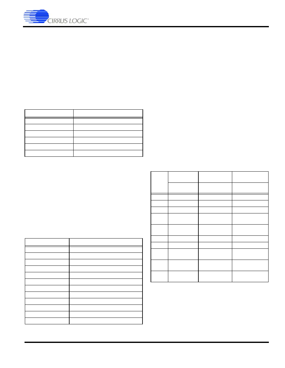
Universal Platform
System-on-chip Processor
EP9312 Data Sheet
FEATURES
∑ 200-MHz ARM920T Processor
∑ 16-kbyte Instruction Cache
∑ 16-kbyte Data Cache
∑ Linux
Æ
, Microsoft
Æ
Windows
Æ
CE-enabled MMU
∑ 100-MHz System Bus
∑ MaverickCrunch
TM
Math Engine
∑ Floating Point, Integer, and Signal Processing
Instructions
∑ Optimized for digital music compression and
decompression algorithms.
∑ Hardware interlocks allow in-line coding.
∑ MaverickKey
TM
IDs
∑ 32-bit unique ID can be used for DRM-compliant,
128-bit random ID.
∑ Integrated Peripheral Interfaces
∑ 32-bit SDRAM Interface (up to 4 banks)
∑ 32/16-bit SRAM / FLASH / ROM
∑ Serial EEPROM Interface
∑ EIDE (up to 2 devices)
∑ 1/10/100 Mbps Ethernet MAC
∑ Three UARTs
∑ Three-port USB 2.0 Full-speed Host (OHCI)
(12 Mbits per second)
∑ LCD and Raster Interface
∑ Touchscreen Interface with ADC
∑ IrDA Interface
∑ 8 x 8 Keypad Scanner
∑ One Serial Peripheral Interface (SPI) Port
∑ 6-channel or 2-channel Serial Audio Interface (I
2
S)
∑ 2-channel, Low-cost Serial Audio Interface (AC'97)
∑ 2 High-resolution PWMs (16 bits each)
∑ Internal Peripherals
∑ 12 Direct Memory Access (DMA) Channels
∑ Real-time Clock with Software Trim
∑ Dual PLL controls all clock domains.
∑ Watchdog Timer
∑ Two General-purpose 16-bit Timers
∑ One General-purpose 32-bit Timer
∑ One 40-bit Debug Timer
∑ Interrupt Controller
∑ Boot ROM
∑ Package
∑ 352 pin PBGA
C
O
MMUNICATIONS P
O
RTS
US
ER INTERFACE
MEMORY AND STORAGE
Unified
SDRAM I/F
Video/LCD
Controller
(3) USB
Hosts
EIDE
I/F
Ethernet
MAC
Bus
Bridge
Boot
ROM
MaverickLock
TM
DMA w/
CRC
SRAM &
Flash I/F
MaverickCrunch
TM
ARM920T
MMU
D-Cache
16KB
I-Cache
16KB
Processor Bus
Peripheral Bus
Serial
Audio
Interface
Interrupts
& GPIO
Clocks &
Timers
Keypad &
Touch
Screen I/F
(3) UARTs
w/
IrDA
12 CHANNEL
DMA
MaverickKey
TM
2
©
Copyright 2005 Cirrus Logic (All Rights Reserved)
DS515PP7
EP9312
Universal Platform SOC Processor
The EP9312 is an ARM920T-based system-on-a-chip
design with a large peripheral set targeted to a variety of
applications:
∑ Thin client computers for business and home
∑ Internet radio
∑ Internet access devices
∑ Industrial computers
∑ Specialized terminals
∑ Point of sale terminals
∑ Test and measurement equipment
The ARM920T microprocessor core with separate 16-
kbyte, 64-way set-associative instruction and data
caches is augmented by the MaverickCrunchTM co-
processor enabling high-speed floating point
calculations.
MaverickKey
TM
unique hardware programmed IDs are a
solution to the growing concern over secure web content
and commerce. With Internet security playing an
important role in the delivery of digital media such as
books or music, traditional software methods are quickly
becoming unreliable. The MaverickKey unique IDs
provide OEMs with a method of utilizing specific
hardware IDs such as those assigned for SDMI (Secure
Digital Music Initiative) or any other authentication
mechanism.
A high-performance 1/10/100 Mbps Ethernet media
access Controller (EMAC) is included along with external
interfaces to SPI, I
2
S audio, Raster/LCD, IDE storage
peripherals, keypad, and touchscreen. A three-port USB
2.0 Full-speed Host (OHCI) (12 Mbits per second) and
three UARTs are included as well.
The EP9312 is a high-performance, low-power, RISC-
based, single-chip computer built around an ARM920T
microprocessor core with a maximum operating clock
rate of 200 MHz (184 MHz for industrial conditions). The
ARM core operates from a 1.8 V supply, while the I/O
operates at 3.3 V with power usage between 100 mW
and 750 mW (dependent on speed).
OVERVIEW
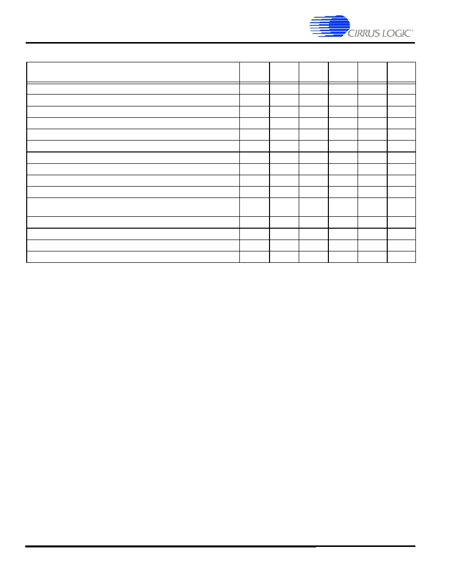
Table A. Change History
Revision
Date
Changes
1
March 2001
Initial Release.
2
June 2001
Upgrade to revision B silicon.
3
August 2001
Upgrade to revision C silicon.
4
May 2003
Upgrade to revision D silicon.
5
December 2003
Update timing data.
6
July 2004
Update AC data.
Add ADC data.
7
Febuary 2005
Update with most-current characterization data.

DS515PP7
©
Copyright 2005 Cirrus Logic (All Rights Reserved)
3
EP9312
Universal Platform SOC Processor
Table of Contents
FEATURES .........................................................................................................1
Overview .............................................................................................................2
Processor Core - ARM920T ......................................................................................... 6
MaverickCrunchTM Math Engine .................................................................................. 6
MaverickKeyTM Unique ID ............................................................................................ 6
General Purpose Memory Interface (SDRAM, SRAM, ROM, FLASH) ........................ 6
IDE Interface ................................................................................................................ 7
Ethernet Media Access Controller (MAC) .................................................................... 7
Serial Interfaces (SPI, I2S, and AC '97) ....................................................................... 7
Raster/LCD Interface ................................................................................................... 7
Touch Screen Interface with 12-bit Analog-to-digital Converter (ADC) ........................ 8
64-Key Keypad Interface ............................................................................................. 8
Universal Asynchronous Receiver/Transmitters (UARTs) ............................................ 8
Triple-port USB Host .................................................................................................... 9
Two-Wire Interface ....................................................................................................... 9
Real-time Clock with Software Trim ............................................................................. 9
PLL and Clocking ......................................................................................................... 9
Timers ........................................................................................................................ 10
Interrupt Controller ..................................................................................................... 10
Dual LED Drivers ....................................................................................................... 10
General Purpose Input/Output (GPIO) ....................................................................... 10
Reset and Power Management ................................................................................. 10
Hardware Debug Interface ..........................................................................................11
12-Channel DMA Controller ........................................................................................11
Internal Boot ROM ......................................................................................................11
Electrical Specifications .................................................................................12
Absolute Maximum Ratings ....................................................................................... 12
Recommended Operating Conditions ........................................................................ 12
DC Characteristics ..................................................................................................... 13
Timings .............................................................................................................14
Memory Interface ....................................................................................................... 15
IDE Interface .............................................................................................................. 30
Ethernet MAC Interface ............................................................................................ 43
Audio Interface ........................................................................................................... 45
AC'97 ........................................................................................................................ 49
LCD Interface ............................................................................................................ 50
ADC ........................................................................................................................... 51
JTAG .......................................................................................................................... 52
352 Pin BGA Package Outline .......................................................................53
352-Ball PBGA Diagram .................................................................................. 53
352 Pin BGA Pinout (Bottom View) ........................................................................... 54
Acronyms and Abbreviations ........................................................................61
Units of Measurement .....................................................................................61
Ordering Information ......................................................................................62

4
©
Copyright 2005 Cirrus Logic (All Rights Reserved)
DS515PP7
EP9312
Universal Platform SOC Processor
List of Figures
Figure 1. Timing Diagram Drawing Key .................................................................................14
Figure 2. SDRAM Load Mode Register Cycle Timing Measurement ..................................... 15
Figure 3. SDRAM Burst Read Cycle Timing Measurement ................................................... 16
Figure 4. SDRAM Burst Write Cycle Timing Measurement ................................................... 17
Figure 5. SDRAM Auto Refresh Cycle Timing Measurement ................................................ 18
Figure 6. Static Memory Single Word Read Cycle Timing Measurement .............................. 19
Figure 7. Static Memory Single Word Write Cycle Timing Measurement .............................. 20
Figure 8. Static Memory Multiple Word Read 8-bit Cycle Timing Measurement .................... 21
Figure 9. Static Memory Multiple Word Write 8-bit Cycle Timing Measurement .................... 22
Figure 10. Static Memory Multiple Word Read 16-bit Cycle Timing Measurement ................ 23
Figure 11. Static Memory Multiple Word Write 16-bit Cycle Timing Measurement ................ 24
Figure 12. Static Memory Burst Read Cycle Timing Measurement .......................................25
Figure 13. Static Memory Burst Write Cycle Timing Measurement .......................................26
Figure 14. Static Memory Single Read Wait Cycle Timing Measurement ............................. 27
Figure 15. Static Memory Single Write Wait Cycle Timing Measurement .............................. 28
Figure 16. Static Memory Turnaround Cycle Timing Measurement .......................................29
Figure 17. Register Transfer to/from Device .......................................................................... 31
Figure 18. PIO Data Transfer to/from Device ......................................................................... 33
Figure 19. Initiating an Ultra DMA data-in Burst ..................................................................... 35
Figure 20. Sustained Ultra DMA data-in Burst ....................................................................... 36
Figure 21. Host Pausing an Ultra DMA data-in Burst ............................................................. 36
Figure 22. Device Terminating an Ultra DMA data-in Burst ................................................... 37
Figure 23. Host Terminating an Ultra DMA data-in Burst ....................................................... 38
Figure 24. Initiating an Ultra DMA data-out Burst .................................................................. 39
Figure 25. Sustained Ultra DMA data-out Burst ..................................................................... 40
Figure 26. Device Pausing an Ultra DMA data-out Burst ....................................................... 40
Figure 27. Host Terminating an Ultra DMA data-out Burst ....................................................41
Figure 28. Device Terminating an Ultra DMA data-out Burst ................................................. 42
Figure 29. Ethernet MAC Timing Measurement ..................................................................... 44
Figure 30. TI Single Transfer Timing Measurement ............................................................... 46
Figure 31. Microwire Frame Format, Single Transfer ............................................................ 46
Figure 32. SPI Format with SPH=1 Timing Measurement ..................................................... 47
Figure 33. Inter-IC Sound (I2S) Timing Measurement ........................................................... 48
Figure 34. AC `97 Configuration Timing Measurement .......................................................... 49
Figure 35. LCD Timing Measurement .................................................................................... 50
Figure 36. ADC Transfer Function ......................................................................................... 51
Figure 37. JTAG Timing Measurement .................................................................................. 52
Figure 38. 352 Pin PBGA Pin Diagram .................................................................................. 53
Figure 40. 352 PIN BGA PINOUT ................................................................................... 55

DS515PP7
©
Copyright 2005 Cirrus Logic (All Rights Reserved)
5
EP9312
Universal Platform SOC Processor
List of Tables
Table A. Change History .......................................................................................................... 2
Table B. General Purpose Memory Interface Pin Assignments .............................................. 6
Table C. IDE Interface Pin Assignments .................................................................................. 7
Table D. Ethernet Media Access Controller Pin Assignments ................................................. 7
Table E. Audio Interfaces Pin Assignment .............................................................................. 7
Table F. LCD Interface Pin Assignments ................................................................................ 8
Table G. Touch Screen Interface with 12-bit Analog-to-Digital Converter Pin Assignments ... 8
Table H. 64-Key Keypad Interface Pin Assignments ............................................................... 8
Table I. Universal Asynchronous Receiver/Transmitters Pin Assignments ............................ 9
Table J. Triple Port USB Host Pin Assignments ..................................................................... 9
Table K. Two-Wire Port with EEPROM Support Pin Assignments .......................................... 9
Table L. Real-Time Clock with Pin Assignments ..................................................................... 9
Table M.PLL and Clocking Pin Assignments ........................................................................ 10
Table N. Interrupt Controller Pin Assignment ........................................................................ 10
Table O. Dual LED Pin Assignments ..................................................................................... 10
Table P. General Purpose Input/Output Pin Assignment ...................................................... 10
Table Q. Reset and Power Management Pin Assignments ................................................... 10
Table R. Hardware Debug Interface ...................................................................................... 11
Table R. 352 Pin Diagram Dimensions .................................................................................. 54
Table S. Pin Descriptions ..................................................................................................... 59
Table T. Pin Multiplex Usage Information ............................................................................. 60
6
©
Copyright 2005 Cirrus Logic (All Rights Reserved)
DS515PP7
EP9312
Universal Platform SOC Processor
Processor Core - ARM920T
The ARM920T is a Harvard architecture processor with
separate 16-kbyte instruction and data caches with an 8-
word line length but a unified memory. The processor
utilizes a five-stage pipeline consisting of fetch, decode,
execute, memory, and write stages. Key features include:
∑ ARM (32-bit) and Thumb (16-bit compressed)
Instruction Sets
∑ 32-bit Advanced Microcontroller Bus Architecture
(AMBA)
∑ 16-kbyte Instruction Cache with lockdown
∑ 16-kbyte Data Cache (programmable write-through or
write-back) with Lockdown
∑ MMU for Linux
Æ
, Microsoft
Æ
Windows
Æ
CE, and other
operating systems
∑ Translation Look Aside Buffers with 64 Data and 64
Instruction Entries
∑ Programmable Page Sizes of 1 Mbyte, 64 kbyte,
4 kbyte, and 1 kbyte
∑ Independent lockdown of TLB Entries
MaverickCrunch
TM
Math Engine
The MaverickCrunch Engine is a mixed-mode
coprocessor designed primarily to accelerate the math
processing required to rapidly encode digital audio
formats. It accelerates single- and double-precision
integer and floating point operations plus an integer
multiply-accumulate (MAC) instruction that is
considerably faster than the ARM920T's native MAC
instruction. The ARM920T coprocessor interface is
utilized thereby sharing its memory interface and
instruction stream. Hardware forwarding and interlock
allows the ARM to handle looping and addressing while
MaverickCrunch handles computation. Features include:
∑ IEEE-754 single and double-precision floating point
∑ 32 / 64-bit integer
∑ Add / multiply / compare
∑ Integer MAC 32-bit input with 72-bit accumulate
∑ Integer Shifts
∑ Floating point to/from integer conversion
∑ Sixteen 64-bit register files
∑ Four 72-bit accumulators
MaverickKey
TM
Unique ID
MaverickKey unique hardware programmed IDs are a
solution to the growing concern over secure web content
and commerce. With Internet security playing an
important role in the delivery of digital media such as
books or music, traditional software methods are quickly
becoming unreliable. The MaverickKey unique IDs
provide OEMs with a method of utilizing specific
hardware IDs such as those assigned for SDMI (Secure
Digital Music Initiative) or any other authentication
mechanism.
Both a specific 32-bit ID as well as a 128-bit random ID
are programmed into the EP9312 through the use of
laser probing technology. These IDs can then be used to
match secure copyrighted content with the ID of the
target device the EP9312 is powering, and then deliver
the copyrighted information over a secure connection. In
addition, secure transactions can benefit by also
matching device IDs to server IDs. MaverickKey IDs
provide a level of hardware security required for today's
Internet appliances.
General Purpose Memory Interface (SDRAM,
SRAM, ROM, FLASH)
The EP9312 features a unified memory address model
where all memory devices are accessed over a common
address/data bus. A separate internal port is dedicated to
the read-only Raster/LCD refresh engine, while the rest
of the memory accesses are performed via the Processor
bus. The SRAM memory controller supports 8, 16 and
32-bit devices and accommodates an internal boot ROM
concurrently with 32-bit SDRAM memory.
∑ 1 to 4 banks of 32-bit, 66- or 100-MHz SDRAM
∑ One internal port dedicated to the Raster/LCD
Refresh Engine (Read Only)
∑ Address and data bus shared between SDRAM,
SRAM, ROM, and FLASH memory
∑ NOR FLASH memory supported
Table B. General Purpose Memory Interface Pin Assignments
Pin Mnemonic
Pin Description
SDCLK
SDRAM Clock
SDCLKEN
SDRAM Clock Enable
SDCSn[3:0]
SDRAM Chip Selects 3-0
RASn
SDRAM RAS
CASn
SDRAM CAS
SDWEn
SDRAM Write Enable
CSn[7:6] and CSn[3:0]
Chip Selects 7, 6, 3, 2, 1, 0
AD[25:0]
Address Bus 25-0
DA[31:0]
Data Bus 31-0
DQMn[3:0]
SDRAM Output Enables / Data Masks
WRn
SRAM Write Strobe
RDn
SRAM Read / OE Strobe
WAITn
SRAM Wait Input
DS515PP7
©
Copyright 2005 Cirrus Logic (All Rights Reserved)
7
EP9312
Universal Platform SOC Processor
IDE Interface
The IDE Interface provides an industry-standard
connection to two AT Advanced Packet Interface (ATAPI)
compliant devices. The IDE port will attach to a master
and a slave device. The internal DMA controller performs
all data transfers using the Multiword DMA and Ultra
DMA modes. The interface supports the following
operating modes:
∑ PIO Modes 0 thru 4
∑ Ultra DMA Modes 0 thru 3
Ethernet Media Access Controller (MAC)
The MAC subsystem is compliant with the ISO/TEC
802.3 topology for a single shared medium with several
stations. Multiple MII-compliant PHYs are supported.
Features include:
∑ Supports 1/10/100 Mbps transfer rates for home /
small-business / large-business applications
∑ Interfaces to an off-chip PHY through industry
standard Media Independent Interface (MII)
Serial Interfaces (SPI, I
2
S, and AC '97)
The SPI port can be configured as a master or a slave,
supporting the National Semiconductor
Æ
, Motorola
Æ
, and
Texas Instruments
Æ
signaling protocols.
The AC'97 port supports multiple codecs for multichannel
audio output with a single stereo input. Three I
2
S ports
can be configured to support six-channel, 24-bit audio.
These ports are multiplexed so that I
2
S port 0 will take
over either the AC'97 pins or the SPI pins. The second
and third I2S ports' serial input and serial output pins are
multiplexed with EGPIO[4,5,6,13]. The clocks supplied in
the first I2S port are also used for the second and third
I2S ports.
∑ Normal Mode: One SPI Port and one AC'97 Port
∑ I
2
S on SSP Mode: One AC'97 Port and up to three I
2
S
Ports
∑ I
2
S on AC'97 Mode: One SPI Port and up to three I
2
S
Ports
`
Raster/LCD Interface
The Raster/LCD interface provides data and interface
signals for a variety of display types. It features fully
programmable video interface timing for non-interlaced
flat panel or dual scan displays. Resolutions up to
1024 x 768 are supported from a unified SDRAM based
frame buffer. A 16-bit PWM provides control for LCD
panel contrast.
Table C. IDE Interface Pin Assignments
Pin Mnemonic
Pin Description
DD[15-0]
IDE Data bus
IDEDA[2-0]
IDE Device address
IDECSn[0,1]
IDE Chip Select 0 and 1
DIORn
IDE Read Strobe
DIOWn
IDE Write Strobe
DMACKn
IDE DMA acknowledge
Table D. Ethernet Media Access Controller Pin Assignments
Pin Mnemonic
Pin Description
MDC
Management Data Clock
MDIO
Management Data I/O
RXCLK
Receive Clock
MIIRXD[3:0]
Receive Data
RXDVAL
Receive Data Valid
RXERR
Receive Data Error
TXCLK
Transmit Clock
MIITXD[3:0]
Transmit Data
TXEN
Transmit Enable
TXERR
Transmit Error
CRS
Carrier Sense
CLD
Collision Detect
Table E. Audio Interfaces Pin Assignment
Pin
Name
Normal Mode
I2S on SSP
Mode
I2S on AC'97
Mode
Pin
Description
Pin Description Pin Description
SCLK1
SPI Bit Clock
I2S Serial Clock
SPI Bit Clock
SFRM1
SPI Frame Clock I2S Frame Clock
SPI Frame Clock
SSPRX1 SPI Serial Input
I2S Serial Input
SPI Serial Input
SSPTX1
SPI Serial
Output
I2S Serial Output
SPI Serial Output
(No I2S Master
Clock)
ARSTn
AC'97 Reset
AC'97 Reset
I2S Master Clock
ABITCLK AC'97 Bit Clock
AC'97 Bit Clock
I2S Serial Clock
ASYNC
AC'97 Frame
Clock
AC'97 Frame
Clock
I2S Frame Clock
ASDI
AC'97 Serial
Input
AC'97 Serial Input I2S Serial Input
ASDO
AC'97 Serial
Output
AC'97 Serial
Output
I2S Serial Output

8
©
Copyright 2005 Cirrus Logic (All Rights Reserved)
DS515PP7
EP9312
Universal Platform SOC Processor
LCD-specific features include:
∑ Timing and interface signals for digital LCD and TFT
displays
∑ Full programmability for either non-interlaced or dual-
scan color and grayscale flat panel displays
∑ Dedicated data path to SDRAM controller for
improved system performance
∑ Pixel depths of 4, 8, 16, or 24 bits per pixel or 256
levels of grayscale
∑ Hardware Cursor up to 64 x 64 pixels
∑ 256 x 18 Color Lookup Table
∑ Hardware Blinking
∑ 8-bit interface to low-end panel
Touch Screen Interface with 12-bit Analog-
to-digital Converter (ADC)
The touch screen interface performs all sampling,
averaging, ADC range checking, and control for a wide
variety of analog resistive touch screens. This controller
only interrupts the processor when a meaningful change
occurs. The touch screen hardware may be disabled and
the switch matrix and ADC controlled directly if desired.
Features include:
∑ Support for 4-, 5-, 7-, or 8-wire analog resistive touch
screens.
∑ Flexibility - unused lines may be used for temperature
sensing or other functions.
∑ Touch screen interrupt function.
64-Key Keypad Interface
The keypad circuitry scans an 8 x 8 array of 64 normally
open, single-pole switches. Any one or two keys
depressed will be de-bounced and decoded. An interrupt
is generated whenever a stable set of depressed keys is
detected. If the keypad is not utilized, the 16 column/row
pins may be used as general purpose I/O. The Keypad
interface:
∑ Provides scanning, debounce, and decoding for a 64-
key switch array.
∑ Scans an 8-row by 8-column matrix.
∑ May decode 2 keys at once.
∑ Generates an interrupt when a new stable key is
determined.
∑ Also generates a 3-key reset interrupt.
Universal Asynchronous
Receiver/Transmitters (UARTs)
Three 16550-compatible UARTs are supplied. Two
provide asynchronous HDLC (High-level Data Link
Control) protocol support for full duplex transmit and
receive. The HDLC receiver handles framing, address
matching, CRC checking, control-octet transparency, and
optionally passes the CRC to the host at the end of the
packet. The HDLC transmitter handles framing, CRC
generation, and control-octet transparency. The host
must assemble the frame in memory before
transmission. The HDLC receiver and transmitter use the
UART FIFOs to buffer the data streams. A third IrDA
Æ
compatible UART is also supplied.
∑ UART1 supports modem bit rates up to 115.2 Kbps,
supports HDLC and includes a 16 byte FIFO for
Table F. LCD Interface Pin Assignments
Pin Mnemonic
Pin Description
SPCLK
Pixel Clock
P[17:0]
Pixel Data Bus [17:0]
HSYNC / LP
Horizontal
Synchronization / Line Pulse
VCSYNC / FP
Vertical or Composite
Synchronization / Frame Pulse
BLANK
Composite Blank
BRIGHT
Pulse Width Modulated Brightness
Table G. Touch Screen Interface with 12-bit Analog-to-Digital
Converter Pin Assignments
Pin Mnemonic
Pin Description
Xp, Xm
Touch screen ADC X Axis
Yp, Ym
Touch screen ADC Y Axis
SXp, SXm
Touch screen ADC X Axis
Voltage Feedback
SYp, SYm
Touch screen ADC Y Axis
Voltage Feedback
Table H. 64-Key Keypad Interface Pin Assignments
Pin Mnemonic
Pin
Description
Alternative Usage
COL[7:0]
Key Matrix Column
Inputs
General Purpose I/O
ROW[7:0]
Key Matrix Row
Inputs
General Purpose I/O
Table G. Touch Screen Interface with 12-bit Analog-to-Digital
Converter Pin Assignments
Pin Mnemonic
Pin Description
DS515PP7
©
Copyright 2005 Cirrus Logic (All Rights Reserved)
9
EP9312
Universal Platform SOC Processor
receive and a 16 byte FIFO for transmit. Interrupts are
generated on Rx, Tx and modem status change.
∑ UART2 contains an IrDA encoder operating at either
the slow (up to 115 Kbps), medium (0.576 or 1.152
Mbps), or fast (4 Mbps) IR data rates. It also has a 16
byte FIFO for receive and a 16 byte FIFO for transmit.
∑ UART3 supports HDLC and includes a 16 byte FIFO
for receive and a 16 byte FIFO for transmit. Interrupts
are generated on Rx and Tx.
Triple-port USB Host
The USB Open Host Controller Interface (Open HCI)
provides full-speed serial communications ports at a
baud rate of 12 Mbits/sec. Up to 127 USB devices
(printer, mouse, camera, keyboard, etc.) and USB hubs
can be connected to the USB host in the USB "tiered
star" topology.
This includes the following features:
∑ Compliance with the USB 2.0 specification
∑ Compliance with the Open HCI Rev 1.0 specification
∑ Supports both low speed (1.5 Mbps) and full speed
(12 Mbps) USB device connections
∑ Root HUB integrated with 3 downstream USB ports
∑ Transceiver buffers integrated, over-current protection
on ports
∑ Supports power management
∑ Operates as a master on the bus
The Open HCI host controller initializes the master DMA
transfer with the AHB bus:
∑ Fetches endpoint descriptors and transfer descriptors
∑ Accesses endpoint data from system memory
∑ Accesses the HC communication area
∑ Writes status and retire transfer descriptor
Two-wire Interface
The two-wire interface provides communication and
control for synchronous-serial-driven devices.
Real-time Clock with Software Trim
The software trim feature on the real time clock (RTC)
provides software controlled digital compensation of the
32.768 KHz input clock. This compensation is accurate to
±
1.24 sec/month.
Note:
A real time clock must be connected to RTCXTALI or
the EP9312 device will not boot.
PLL and Clocking
The Processor and the Peripheral Clocks operate from a
single 14.7456 MHz crystal.
The Real Time Clock operates from a 32.768 KHz
external oscillator.
Table I. Universal Asynchronous Receiver/Transmitters Pin
Assignments
Pin Mnemonic
Pin Name - Description
TXD0
UART1 Transmit
RXD0
UART1 Receive
CTSn
UART1 Clear To Send /
Transmit Enable
DSRn / DCDn
UART1 Data Set Ready /
Data Carrier Detect
DTRn
UART1 Data Terminal Ready
RTSn
UART1 Ready To Send
EGPIO[0] / RI
UART1 Ring Indicator
TXD1 / SIROUT
UART2 Transmit /
IrDA Output
RXD1 / SIRIN
UART2 Receive / IrDA Input
TXD2
UART3 Transmit
RXD2
UART3 Receive
EGPIO[3] / TENn
HDLC3 Transmit Enable
Table J. Triple Port USB Host Pin Assignments
Pin Mnemonic
Pin Name - Description
USBp[2:0]
USB Positive signals
USBm[2:0]
USB Negative Signals
Table K. Two-Wire Port with EEPROM Support Pin Assignments
Pin Mnemonic
Pin Name - Description
Alternative
Usage
EECLK
Two-wire Interface Clock
General
Purpose I/O
EEDATA
Two-wire Interface Data
General
Purpose I/O
Table L. Real-Time Clock with Pin Assignments
Pin Mnemonic
Pin Name - Description
RTCXTALI
Real-Time Clock Oscillator Input
RTCXTALO
Real-Time Clock Oscillator Output

10
©
Copyright 2005 Cirrus Logic (All Rights Reserved)
DS515PP7
EP9312
Universal Platform SOC Processor
Timers
The Watchdog Timer ensures proper operation by
requiring periodic attention to prevent a reset-on-time-
out.
Two 16-bit timers operate as free-running down counters
or as periodic timers for fixed-interval interrupts and have
a range of 0.03 ms to 4.27 seconds.
One 32-bit timer, plus a 6-bit prescale counter, has a
range of 0.03
µ
s to 73.3 hours.
One 40-bit debug timer, plus a 6-bit prescale counter, has
a range of 1.0
µ
s to 12.7 days.
Interrupt Controller
The interrupt controller allows up to 64 interrupts to
generate an Interrupt Request (IRQ) or Fast Interrupt
Request (FIQ) signal to the processor core. Thirty-two
hardware priority assignments are provided for assisting
IRQ vectoring, and two levels are provided for FIQ
vectoring. This allows time-critical interrupts to be
processed in the shortest time possible. Internal
interrupts may be programmed as active high or active
low level sensitive inputs. External interrupts may be
programmed as active-high level-sensitive, active-low
level-sensitive, rising-edge-triggered, falling-edge-
triggered, or combined rising/falling-edge-triggered.
∑ Supports 64 interrupts from a variety of sources (such
as UARTs, GPIO, and key matrix)
∑ Routes interrupt sources to either the ARM920T's
IRQ or FIQ (Fast IRQ) inputs
∑ Four dedicated off-chip interrupt lines INT[3:0]
operate as level-sensitive interrupts
∑ Any of the 16 GPIO lines maybe configured to
generate interrupts
∑ Software-supported priority mask for all FIQs and
IRQs
Dual LED Drivers
Two pins are assigned specifically to drive external
LEDs.
General Purpose Input/Output (GPIO)
The 16 EGPIO pins may each be configured individually
as an output, an input, or an interrupt input.
There are 23 pins that may alternatively be used as input,
output, but do not support interrupts. These pins are:
∑ Key Matrix ROW[7:0], COL[7:0]
∑ Ethernet MDIO
∑ Both LED Outputs
∑ Two-wire Clock and Data
∑ SLA [1:0]
6 pins may alternatively be used as inputs only:
∑ CTSn, DSRn / DCDn
∑ 4 Interrupt Lines
2 pins may alternatively be used as outputs only:
∑ RTSn
∑ ARSTn
Reset and Power Management
The chip may be reset through the PRSTn pin or through
the open drain common reset pin, RSTOn.
Clocks are managed on a peripheral-by-peripheral basis
and may be turned off to conserve power.
The processor clock is dynamically adjustable from 0 to
200 MHz (184 MHz for industrial conditions).
Table M. PLL and Clocking Pin Assignments
Pin Mnemonic
Pin Name - Description
XTALI
Main Oscillator Input
XTALO
Main Oscillator Output
VDD_PLL
Main Oscillator Power
GND_PLL
Main Oscillator Ground
Table N. External Interrupt Controller Pin Assignment
Pin Mnemonic
Pin Name - Description
INT[3:0]
External Interrupt 3-0
Table O. Dual LED Pin Assignments
Pin Mnemonic
Pin Name -
Description
Alternative Usage
GRLED
Green LED
General Purpose I/O
REDLED
Red LED
General Purpose I/O
Table P. General Purpose Input/Output Pin Assignment
Pin Mnemonic
Pin Name - Description
EGPIO[15:0]
Expanded General Purpose Input / Output
Pins with Interrupts
Table Q. Reset and Power Management Pin Assignments
Pin Mnemonic
Pin Name - Description
PRSTn
Power On Reset
RSTOn
User Reset In/Out ≠ Open Drain ≠
Preserves Real Time Clock value

DS515PP7
©
Copyright 2005 Cirrus Logic (All Rights Reserved)
11
EP9312
Universal Platform SOC Processor
Hardware Debug Interface
The JTAG interface allows use of ARM's Multi-ICE or
other in-circuit emulators.
12-channel DMA Controller
The DMA module contains 12 separate DMA channels.
Ten of these may be used for peripheral-to-memory or
memory-to-peripheral access. Two of these are
dedicated to memory-to-memory transfers. Each DMA
channel is connected to the 16-bit DMA request bus.
The request bus is a collection of requests, Serial Audio
and UARTs. Each DMA channel can be used
independently or dedicated to any request signal. For
each DMA channel, source and destination addressing
can be independently programmed to increment,
decrement, or stay at the same value. All DMA
addresses are physical, not virtual addresses.
Internal Boot ROM
The Internal 16 Kbyte ROM allows booting from FLASH
memory, SPI or UART. Consult the EP93xx User's Guide
for operational details.
Table R. Hardware Debug Interface
Pin Mnemonic
Pin Name - Description
TCK
JTAG Clock
TDI
JTAG Data In
TDO
JTAG Data Out
TMS
JTAG Test Mode Select
TRSTn
JTAG Port Reset
12
©
Copyright 2005 Cirrus Logic (All Rights Reserved)
DS515PP7
EP9312
Universal Platform SOC Processor
Electrical Specifications
Absolute Maximum Ratings
Note:
1. Includes all power generated by AC and/or DC output loading.
2. The power supply pins are at recommended maximum values.
3. At ambient temperatures above 70∞ C, total power dissipation must be limited to less than 2.5 Watts.
WARNING: Operation beyond these limits may result in permanent damage to the device.
Normal operation is not guaranteed at these extremes.
Recommended Operating Conditions
(All grounds = 0 V, all voltages with respect to 0 V)
Parameter
Symbol
Min
Max
Unit
Power Supplies
RVDD
CVDD
VDD_PLL
VDD_ADC
-
-
-
-
3.96
2.16
2.16
3.96
V
V
V
V
Total Power Dissipation
(Note 1)
-
2
W
Input Current per Pin, DC (Except supply pins)
-
±10
mA
Output current per pin, DC
-
±50
mA
Digital Input voltage
(Note 2)
-0.3
RVDD+0.3
V
Storage temperature
-40
+125
∞C
(All grounds = 0 V, all voltages with respect to 0 V)
Parameter
Symbol
Min
Typ
Max
Unit
Power Supplies
RVDD
CVDD
VDD_PLL
VDD_ADC
3.0
1.65
1.65
3.0
3.3
1.80
1.80
3.3
3.6
1.94
1.94
3.6
V
V
V
V
Operating Ambient Temperature - Commercial
T
A
0
+25
+70
∞C
Operating Ambient Temperature - Industrial
T
A
-40
+25
+85
∞C
Processor Clock Speed - Commercial
FCLK
-
-
200
MHz
Processor Clock Speed - Industrial
FCLK
-
-
184
MHz
System Clock Speed - Commercial
HCLK
-
-
100
MHz
System Clock Speed - Industrial
HCLK
-
-
92
MHz
DS515PP7
©
Copyright 2005 Cirrus Logic (All Rights Reserved)
13
EP9312
Universal Platform SOC Processor
DC Characteristics
Note:
4. For open drain pins, high level output voltage is dependent on the external load.
5. All inputs that do not include internal pull-ups or pull-downs, must be externally driven for proper operation (See
Table S on
page 59
). If an input is not driven, it should be tied to power or ground, depending on the particular function. If an I/O pin is not
driven and programmed as an input, it should be tied to power or ground through its own resistor.
(T
A
= 0 to 70∞ C; CVDD = VDD_PLL = 1.8; RVDD = 3.3 V;
All grounds = 0 V; all voltages with respect to 0 V unless otherwise noted)
Parameter
Symbol
Min
Max
Unit
High level output voltage
Iout = -4 mA
(Note 4)
V
oh
0.85
◊
RVDD
-
V
Low level output voltage
Iout = 4 mA
V
ol
-
0.15
◊
RVDD
V
High level input voltage
(Note 5)
V
ih
0.65
◊
RVDD
VDD + 0.3
V
Low level input voltage
(Note 5)
V
il
-0.3
0.35
◊
RVDD
V
High level leakage current
Vin = 3.3 V
(Note 5)
I
ih
-
10
µA
Low level leakage current
Vin = 0
(Note 5)
I
il
-
-10
µA
Parameter
Min
Typ
Max
Unit
Power Supply Pins (Outputs Unloaded)
Power Supply Current:
CVDD / VDD_PLL Total
RVDD
-
-
190
45
240
80
mA
mA
Low-Power Mode Supply Current
CVDD / VDD_PLL Total
RVDD
-
-
2
1.0
3.5
2
mA
mA

14
©
Copyright 2005 Cirrus Logic (All Rights Reserved)
DS515PP7
EP9312
Universal Platform SOC Processor
Timings
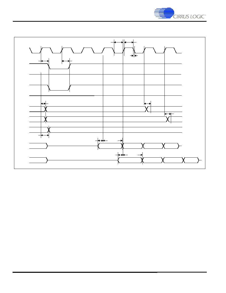
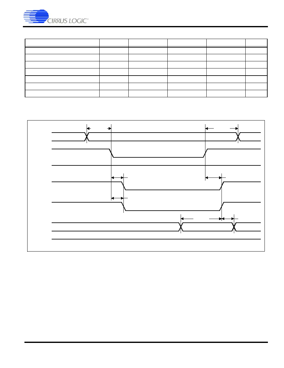
Timing Diagram Conventions
This data sheet contains one or more timing diagrams. The following key explains the components used in these
diagrams. Any variations are clearly labelled when they occur. Therefore, no additional meaning should be attached
unless specifically stated.
Figure 1. Timing Diagram Drawing Key
Timing Conditions
Unless specified otherwise, the following conditions are true for all timing measurements.
∑ T
A
= 0 to 70∞ C
∑ CVDD = VDD_PLL = 1.8V
∑ RVDD = 3.3 V
∑ All grounds = 0 V
∑ Logic 0 = 0 V, Logic 1 = 3.3 V
∑ Output loading = 50 pF
∑ Timing reference levels = 1.5 V
∑ The Processor Bus Clock (HCLK) is programmable and is set by the user. The frequency is typically between
33 MHz and 100 MHz (92 MHz for industrial conditions).
Clock
High to Low
High/Low to High
Bus Change
Bus Valid
Undefined/Invalid
Valid Bus to Tristate
Bus/Signal Omission

DS515PP7
©
Copyright 2005 Cirrus Logic (All Rights Reserved)
15
EP9312
Universal Platform SOC Processor
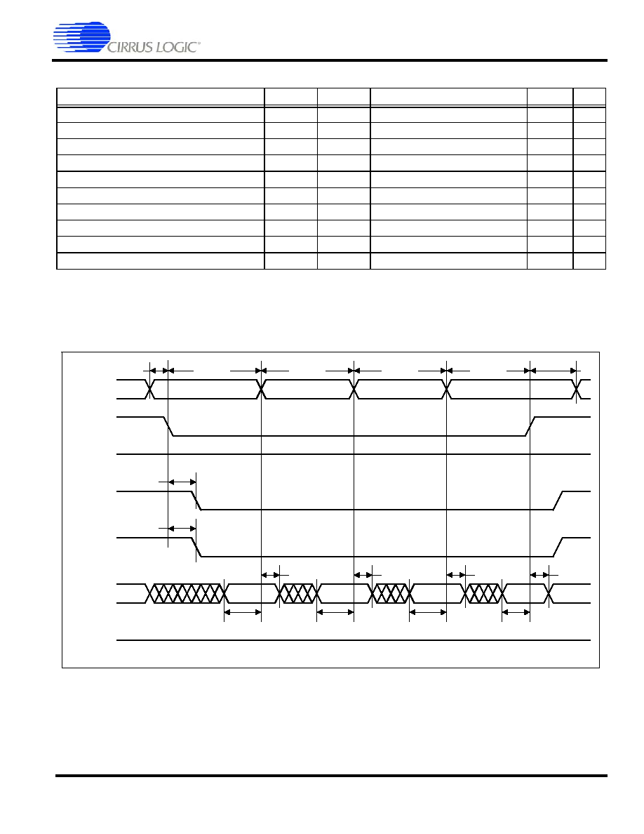
Memory Interface
SDRAM Load Mode Register Cycle
Figure 2
through
Figure 5
define the timings associated with all phases of the SDRAM. The following table contains the
values for the timings of each of the SDRAM modes.
Parameter
Symbol
Min
Typ
Max
Unit
SDCLK high time
t
clk_high
-
(t
HCLK
) / 2
-
ns
SDCLK low time
t
clk_low
-
(t
HCLK
) / 2
-
ns
SDCLK rise/fall time
t
clkrf
-
2
4
ns
Signal delay from SDCLK rising edge time
t
d
-
-
8
ns
Signal hold from SDCLK rising edge time
t
h
1
-
-
ns
DQMn delay from SDCLK rising edge time
t
DQd
-
-
8
ns
DQMn hold from SDCLK rising edge time
t
DQh
1
-
-
ns
DA valid setup to SDCLK rising edge time
t
DAs
2
-
-
ns
DA valid hold from SDCLK rising edge time
t
DAh
3
-
-
ns
Figure 2. SDRAM Load Mode Register Cycle Timing Measurement
SDCLK
SDCSn
RASn
CASn
SDWEn
DQMn
AD
DA
OP-Code
t
clk_high
t
clk_low
t
clkrf
t
d
t
h
16
©
Copyright 2005 Cirrus Logic (All Rights Reserved)
DS515PP7
EP9312
Universal Platform SOC Processor
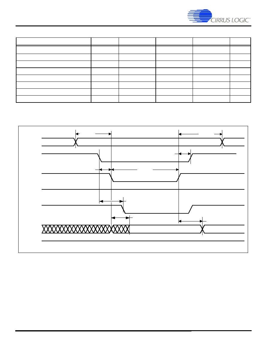
SDRAM Burst Read Cycle
Figure 3. SDRAM Burst Read Cycle Timing Measurement
n
n + 1
n + 2
n + 3
SDCLK
SDCSn
RASn
CASn
SDWEn
DQMn
CL = 2
AD
DA
CL = 2
t
DAs
t
clk_low
t
clk_high
t
clkrf
t
d
t
d
t
h
t
DAh
t
DQh
t
DQd
n
n + 1
n + 2
n + 3
t
DAs
t
DAh
DA
CL = 3
DQMn
CL = 3
t
DQh
DS515PP7
©
Copyright 2005 Cirrus Logic (All Rights Reserved)
17
EP9312
Universal Platform SOC Processor
SDRAM Burst Write Cycle
Figure 4. SDRAM Burst Write Cycle Timing Measurement
SDCLK
SDCSn
RASn
CASn
SDWEn
DQMn
AD
DA
t
clk_low
t
clk_high
t
clkrf
t
d
t
h
t
h
n
n +1
n + 2
n + 3

18
©
Copyright 2005 Cirrus Logic (All Rights Reserved)
DS515PP7
EP9312
Universal Platform SOC Processor
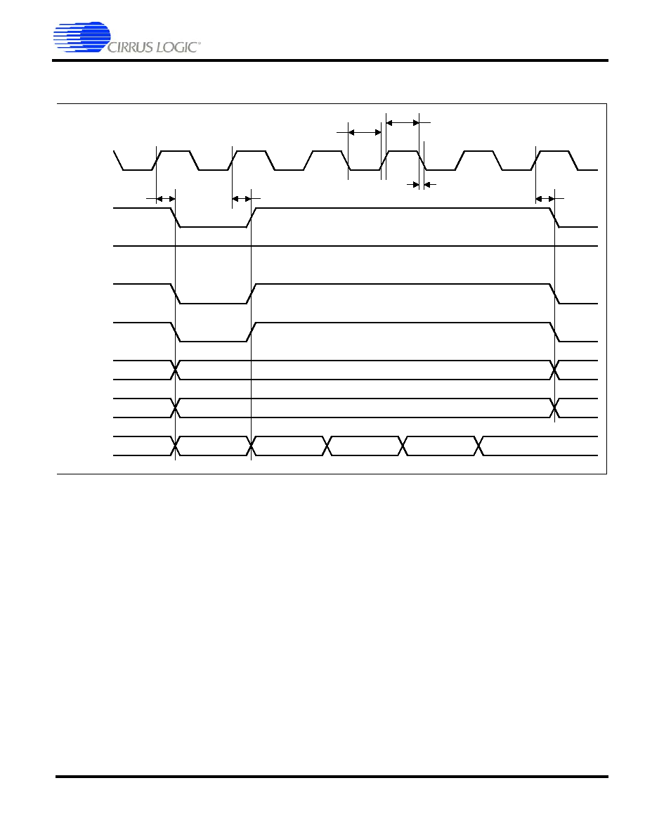
SDRAM Auto Refresh Cycle
Note:
Chip select shown as bus to illustrate multiple devices being put into auto refresh in one access
Figure 5. SDRAM Auto Refresh Cycle Timing Measurement
SDCLK
SDCSn
RASn
CASn
SDWEn
t
clk_low
t
clk_high
7
b
d
e
t
d
t
h
t
clkrf
DS515PP7
©
Copyright 2005 Cirrus Logic (All Rights Reserved)
19
EP9312
Universal Platform SOC Processor
Static Memory Single Word Read Cycle
See
"Timing Conditions" on page 14
for definition of HCLK.
Parameter
Symbol
Min
Typ
Max
Unit
AD setup to CSn assert time
t
ADs
0
-
-
ns
AD hold from CSn deassert time
t
ADh
t
HCLK
-
-
ns
RDn assert time
t
RDpw
-
t
HCLK
◊
(WST1 + 2)
-
ns
CSn to RDn delay time
t
RDd
-
-
3
ns
CSn assert to DQMn assert delay time
t
DQMd
-
-
1
ns
DA setup to RDn deassert time
t
DAs
t
HCLK
+
12
-
-
ns
DA hold from RDn deassert time
t
DAh
0
-
-
ns
Figure 6. Static Memory Single Word Read Cycle Timing Measurement
CSn
WRn
RDn
DQMn
AD
DA
t
ADs
t
RDd
t
DQMd
t
ADh
t
RDd
t
DAs
t
DAh
WAIT
20
©
Copyright 2005 Cirrus Logic (All Rights Reserved)
DS515PP7
EP9312
Universal Platform SOC Processor
Static Memory Single Word Write Cycle
Parameter
Symbol
Min
Typ
Max
Unit
AD setup to WRn assert time
t
ADs
t
HCLK
-
3
-
-
ns
AD hold from WRn deassert time
t
ADh
t
HCLK
◊
2
-
-
ns
WRn deassert to CSn deassert time
t
CSh
7
-
-
ns
CSn to WRn assert delay time
t
WRd
-
-
2
ns
WRn assert time
t
WRpw
-
t
HCLK
◊
(WST1 + 1)
-
ns
CSn to DQMn assert delay time
t
DQMd
-
-
1
ns
WRn deassert to DA transition time
t
DAh
t
HCLK
-
-
ns
WRn assert to DA valid
t
DAV
-
-
8
ns
Figure 7. Static Memory Single Word Write Cycle Timing Measurement
CSn
WRn
RDn
DQMn
AD
DA
t
ADs
t
ADh
t
CSh
t
WRd
t
WRpw
t
DAh
WAIT
t
DQMd
t
DAV
DS515PP7
©
Copyright 2005 Cirrus Logic (All Rights Reserved)
21
EP9312
Universal Platform SOC Processor
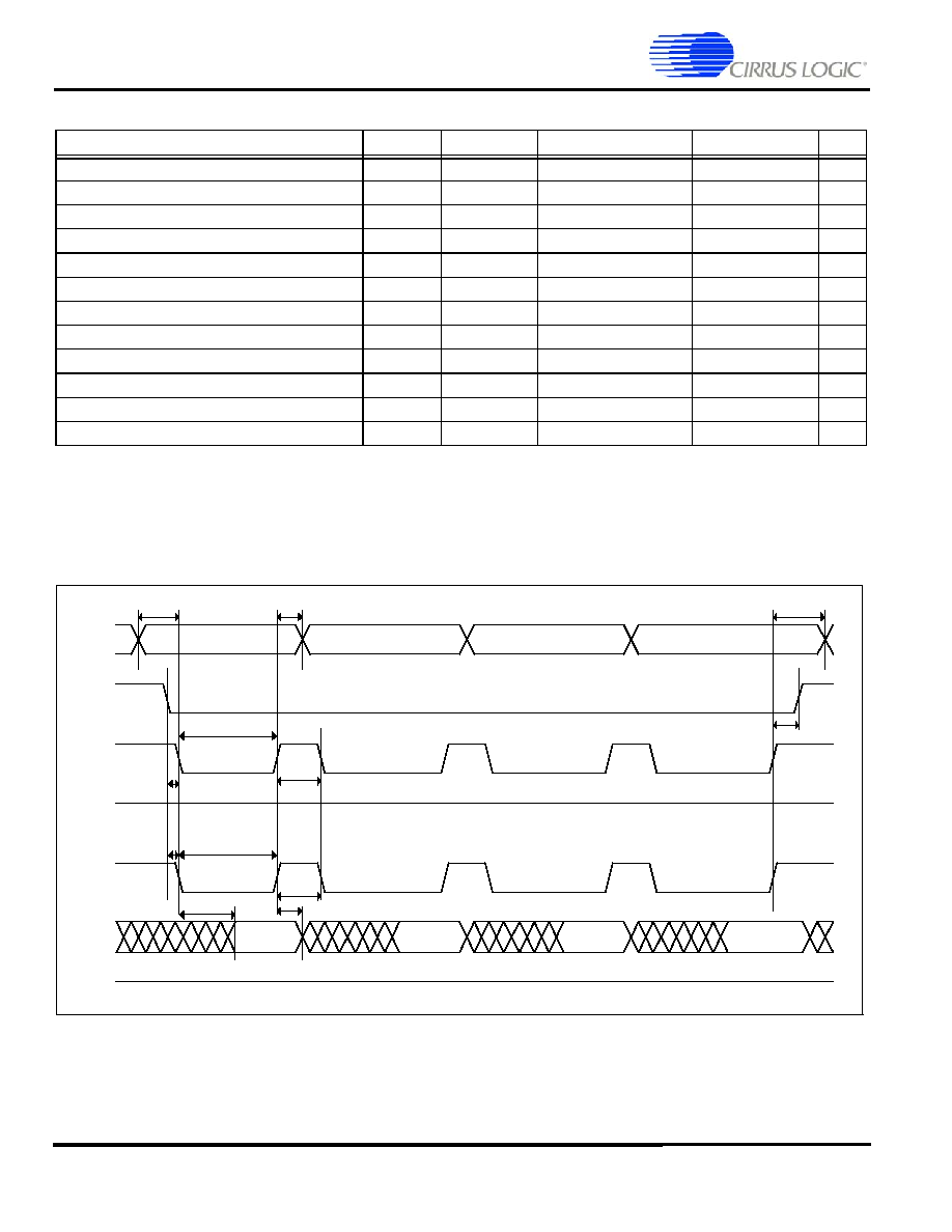
Static Memory 32-bit Read on 8-bit External Bus
Parameter
Symbol
Min
Typ
Max
Unit
AD setup to CSn assert time
t
ADs
t
HCLK
-
-
ns
CSn assert to Address transition time
t
AD1
-
t
HCLK
◊
(WST1 + 1)
-
ns
Address assert time
t
AD2
-
t
HCLK
◊
(WST1 + 1)
-
ns
AD transition to CSn deassert time
t
AD3
-
t
HCLK
◊
(WST1 + 2)
-
ns
AD hold from CSn deassert time
t
ADh
t
HCLK
-
-
ns
RDn assert time
t
RDpwL
-
t
HCLK
◊
(4
◊
WST1 + 5)
-
ns
CSn to RDn delay time
t
RDd
-
-
3
ns
CSn assert to DQMn assert delay time
t
DQMd
-
-
1
ns
DA setup to AD transition time
t
DAs1
15
-
-
ns
DA setup to RDn deassert time
t
DAs2
t
HCLK
+
12
-
-
ns
DA hold from AD transition time
t
DAh1
0
-
-
ns
DA hold from RDn deassert time
t
DAh2
0
-
-
ns
Figure 8. Static Memory Multiple Word Read 8-bit Cycle Timing Measurement
1
CSn
WRn
RDn
DA
AD
DQMn
t
ADs
t
AD1
t
AD2
t
AD2
t
DAs1
t
RDd
t
DAh1
t
DAh1
t
DAh1
t
DAs1
t
DAs1
t
DAs2
t
DAh2
t
ADh
WAIT
t
RDd
t
DQMd
t
AD3

22
©
Copyright 2005 Cirrus Logic (All Rights Reserved)
DS515PP7
EP9312
Universal Platform SOC Processor
Static Memory 32-bit Write on 8-bit External Bus
Parameter
Symbol
Min
Typ
Max
Unit
AD setup to WRn assert time
t
ADs
t
HCLK
-
3
-
-
ns
WRn/DQMn deassert to AD transition time
t
ADd
-
-
t
HCLK
+
6
ns
AD hold from WRn deassert time
t
ADh
t
HCLK
◊
2
-
-
ns
CSn hold from WRn deassert time
t
CSh
7
-
-
ns
CSn to WRn assert delay time
t
WRd
-
-
2
ns
WRn assert time
t
WRpwL
-
t
HCLK
◊
(WST1 + 1)
-
ns
WRn deassert time
t
WRpwH
-
t
HCLK
◊
2
(t
HCLK
◊
2) + 14
ns
CSn to DQMn assert delay time
t
DQMd
-
-
1
ns
DQMn assert time
t
DQMpwL
-
t
HCLK
◊
(WST1 + 1)
-
ns
DQMn deassert time
t
DQMpwH
-
-
(t
HCLK
◊
2) + 7
ns
WRn / DQMn deassert to DA transition time
t
DAh
t
HCLK
-
-
ns
WRn / DQMn assert to DA valid time
t
DAV
-
-
8
ns
Figure 9. Static Memory Multiple Word Write 8-bit Cycle Timing Measurement
CSn
WRn
RDn
DQMn
AD
DA
t
ADs
t
WRd
t
DQMd
t
WRpwL
t
DAh
t
WRpwH
t
ADd
t
CSh
t
ADh
t
DQMpwL
t
DQMpwH
t
WRpwL
t
WRpwH
t
WRpwL
t
WRpwH
t
DQMpwL
t
DQMpwH
t
DQMpwL
t
DQMpwH
t
DAh
t
DAh
t
DAh
t
ADd
t
ADd
WAIT
t
DAV
t
DAV
t
DAV
t
DAV

DS515PP7
©
Copyright 2005 Cirrus Logic (All Rights Reserved)
23
EP9312
Universal Platform SOC Processor
Static Memory 32-bit Read on 16-bit External Bus
Parameter
Symbol
Min
Typ
Max
Unit
AD setup to CSn assert time
t
ADs
t
HCLK
-
-
ns
CSn assert to AD transition time
t
ADd1
-
t
HCLK
◊
(WST1 + 1)
-
ns
AD transition to CSn deassert time
t
ADd2
-
t
HCLK
◊
(WST1 + 2)
-
ns
AD hold from CSn deassert time
t
ADh
t
HCLK
-
-
ns
RDn assert time
t
RDpwL
-
t
HCLK
◊
((2
◊
WST1) + 3)
-
ns
CSn to RDn delay time
t
RDd
-
-
3
ns
CSn assert to DQMn assert delay time
t
DQMd
-
-
1
ns
DA setup to AD transition time
t
DAs1
15
-
-
ns
DA to RDn deassert time
t
DAs2
t
HCLK
+ 12
-
-
ns
DA hold from AD transition time
t
DAh1
0
-
-
ns
DA hold from RDn deassert time
t
DAh2
0
-
-
ns
Figure 10. Static Memory Multiple Word Read 16-bit Cycle Timing Measurement
CSn
WRn
RDn
DA
AD
DQMn
t
RDpwl
t
ADd1
t
RDh
t
DQMh
t
DAh2
t
DAs1
t
DAh1
t
DAs2
WAIT
t
ADs
t
RDd
t
DQMd
t
ADh
t
ADd2
24
©
Copyright 2005 Cirrus Logic (All Rights Reserved)
DS515PP7
EP9312
Universal Platform SOC Processor
Static Memory 32-bit Write on 16-bit External Bus
Parameter
Symbol
Min
Typ
Max
Unit
AD setup to WRn assert time
t
ADs
t
HCLK
≠ 3
-
-
ns
WRn/DQMn deassert to AD transition time
t
ADd
-
-
t
HCLK
+ 6
ns
AD hold from WRn deassert time
t
ADh
t
HCLK
◊ 2
-
-
ns
CSn hold from WRn deassert time
t
CSh
7
-
-
ns
CSn to WRn assert delay time
t
WRd
-
-
2
ns
WRn assert time
t
WRpwL
-
t
HCLK
◊ (WST1 + 1)
-
ns
WRn deassert time
t
WRpwH
-
-
(t
HCLK
◊ 2) + 14
ns
CSn to DQMn assert delay time
t
DQMd
-
-
1
ns
DQMn assert time
t
DQMpwL
-
t
HCLK
◊ (WST1 + 1)
-
ns
DQMn deassert time
t
DQMpwH
-
-
(t
HCLK
◊ 2) + 7
ns
WRn / DQMn deassert to DA transition time
t
DAh1
t
HCLK
-
-
ns
WRn / DQMn assert to DA valid time
t
DAV
-
-
8
ns
Figure 11. Static Memory Multiple Word Write 16-bit Cycle Timing Measurement
CSn
WRn
RDn
DQMn
AD
DA
t
ADs
t
WRd
t
WRpwL
t
DAh
t
ADd
t
WRpwH
t
DQMd
t
ADh
t
DAh
t
WRpwL
t
DQpwL
t
DQpwH
t
DQpwL
WAIT
t
CSh
t
DAV
t
DAV
DS515PP7
©
Copyright 2005 Cirrus Logic (All Rights Reserved)
25
EP9312
Universal Platform SOC Processor
Static Memory Burst Read Cycle
Note:
These characteristics are valid when the Page Mode Enable (Burst Mode) bit is set. See the User's Guide for details.
Parameter
Symbol
Min
Typ
Max
Unit
CSn assert to Address 1 transition time
t
ADd1
-
t
HCLK
◊
(WST1 + 1)
-
ns
Address assert time
t
ADd2
-
t
HCLK
◊
(WST2 + 1)
-
ns
AD transition to CSn deassert time
t
ADd3
-
t
HCLK
◊
(WST1 + 2)
-
ns
AD hold from CSn deassert time
t
ADh
t
HCLK
-
-
ns
CSn to RDn delay time
t
RDd
-
-
3
ns
CSn to DQMn assert delay time
t
DQMd
-
-
1
ns
DA setup to AD transition time
t
DAs1
15
-
-
ns
DA setup to CSn deassert time
t
DAs2
t
HCLK
+ 12
-
-
ns
DA hold from AD transition time
t
DAh1
0
-
-
ns
DA hold from RDn deassert time
t
DAh2
0
-
-
ns
Figure 12. Static Memory Burst Read Cycle Timing Measurement
AD
CSn
WRn
RDn
DQMn
DA
t
ADd1
t
ADd2
t
ADd2
t
RDd
t
DQMd
t
DAs1
t
DAh1
t
DAs1
t
DAh1
t
DAs1
t
DAh1
t
DAs2
t
DAh2
t
ADh
WAIT
t
ADd3
t
ADs
26
©
Copyright 2005 Cirrus Logic (All Rights Reserved)
DS515PP7
EP9312
Universal Platform SOC Processor
Static Memory Burst Write Cycle
Note:
These characteristics are valid when the Page Mode Enable (Burst Mode) bit is set. See the User's Guide for details.
Parameter
Symbol
Min
Typ
Max
Unit
AD setup to WRn assert time
t
ADs
t
HCLK
-
3
ns
AD hold from WRn deassert time
t
ADh
t
HCLK
◊
2
ns
WRN/DQMn deassert to AD transition time
t
ADd
t
HCLK
+ 6
ns
CSn hold from WRn deassert time
t
CSh
7
ns
CSn to WRn assert delay time
t
WRd
2
ns
CSn to DQMn assert delay time
t
DQMd
1
ns
DQMn assert time
t
DQpwL
t
HCLK
◊
(WST1 + 1)
ns
DQMn deassert time
t
DQpwH
(t
HCLK
◊
2) + 14
ns
WRn assert time
t
WRpwL
t
HCLK
◊
(WST1 + 11)
ns
WRn deassert time
t
WRpwH
(t
HCLK
◊
2) + 7
ns
WRn/DQMn deassert to DA transition time
t
DAh
t
HCLK
ns
WRn/DQMn assert to DA valid time
t
DAv
8
ns
Figure 13. Static Memory Burst Write Cycle Timing Measurement
AD
CSn
WRn
RD
DQMn
DA
WAIT
t
ADs
t
ADd
t
WRpwL
t
DQpwL
t
DQpwH
t
WRpwH
t
DAv
t
DAh
t
WRd
t
DQMd
t
CSh
t
ADh

DS515PP7
©
Copyright 2005 Cirrus Logic (All Rights Reserved)
27
EP9312
Universal Platform SOC Processor
Static Memory Single Read Wait Cycle
Parameter
Symbol
Min
Typ
Max
Unit
CSn assert to WAIT time
t
WAITd
-
-
t
HCLK
◊
(WST1-2)
ns
WAIT assert time
t
WAITpw
t
HCLK
◊
2
-
t
HCLK
◊
510
ns
WAIT to CSn deassert delay time
t
CSnd
t
HCLK
◊
3
-
t
HCLK
◊
5
ns
Figure 14. Static Memory Single Read Wait Cycle Timing Measurement
CSn
WRn
RDn
DQMn
AD
DA
WAIT
t
WAITpw
t
WAITd
t
CSnd

28
©
Copyright 2005 Cirrus Logic (All Rights Reserved)
DS515PP7
EP9312
Universal Platform SOC Processor
Static Memory Single Write Wait Cycle
Parameter
Symbol
Min
Typ
Max
Unit
WAIT to WRn deassert delay time
t
WRd
t
HCLK
◊
2
-
t
HCLK
◊
4
ns
CSn assert to WAIT time
t
WAITd
-
-
t
HCLK
◊
(WST1-2)
ns
WAIT assert time
t
WAITpw
t
HCLK
◊
2
-
t
HCLK
◊
510
ns
WAIT to CSn deassert delay time
t
CSnd
t
HCLK
◊
3
-
t
HCLK
◊
5
ns
Figure 15. Static Memory Single Write Wait Cycle Timing Measurement
CSn
WRn
RDn
DQMn
AD
DA
WAIT
t
WAITpw
t
WAITd
t
CSnd
t
WRd
DS515PP7
©
Copyright 2005 Cirrus Logic (All Rights Reserved)
29
EP9312
Universal Platform SOC Processor
Static Memory Turnaround Cycle
Notes: 1. X and Y represent any two chip select numbers.
2. IDCY occurs on read-to-write and write-to-read.
3. IDCY is honored when going from a asynchronous device (CSx) to a synchronous device (/SDCSy).
Parameter
Symbol
Min
Typ
Max
Unit
CSnX deassert to CSnY assert time
t
BTcyc
-
t
HCLK
◊
(IDCY+1)
-
ns
Figure 16. Static Memory Turnaround Cycle Timing Measurement
AD
CSnX
WRn
RDn
DQMn
DA
CSnY
t
BTcyc
WAIT

30
©
Copyright 2005 Cirrus Logic (All Rights Reserved)
DS515PP7
EP9312
Universal Platform SOC Processor
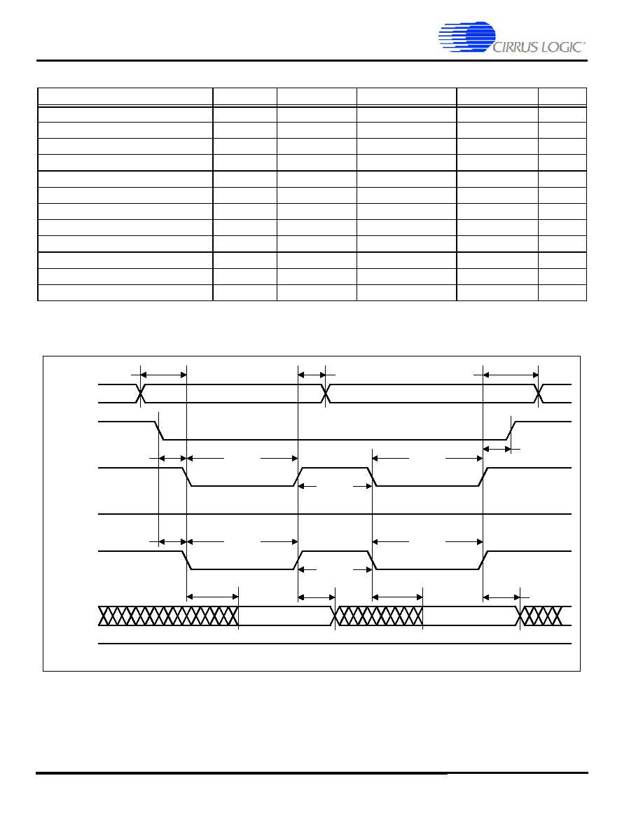
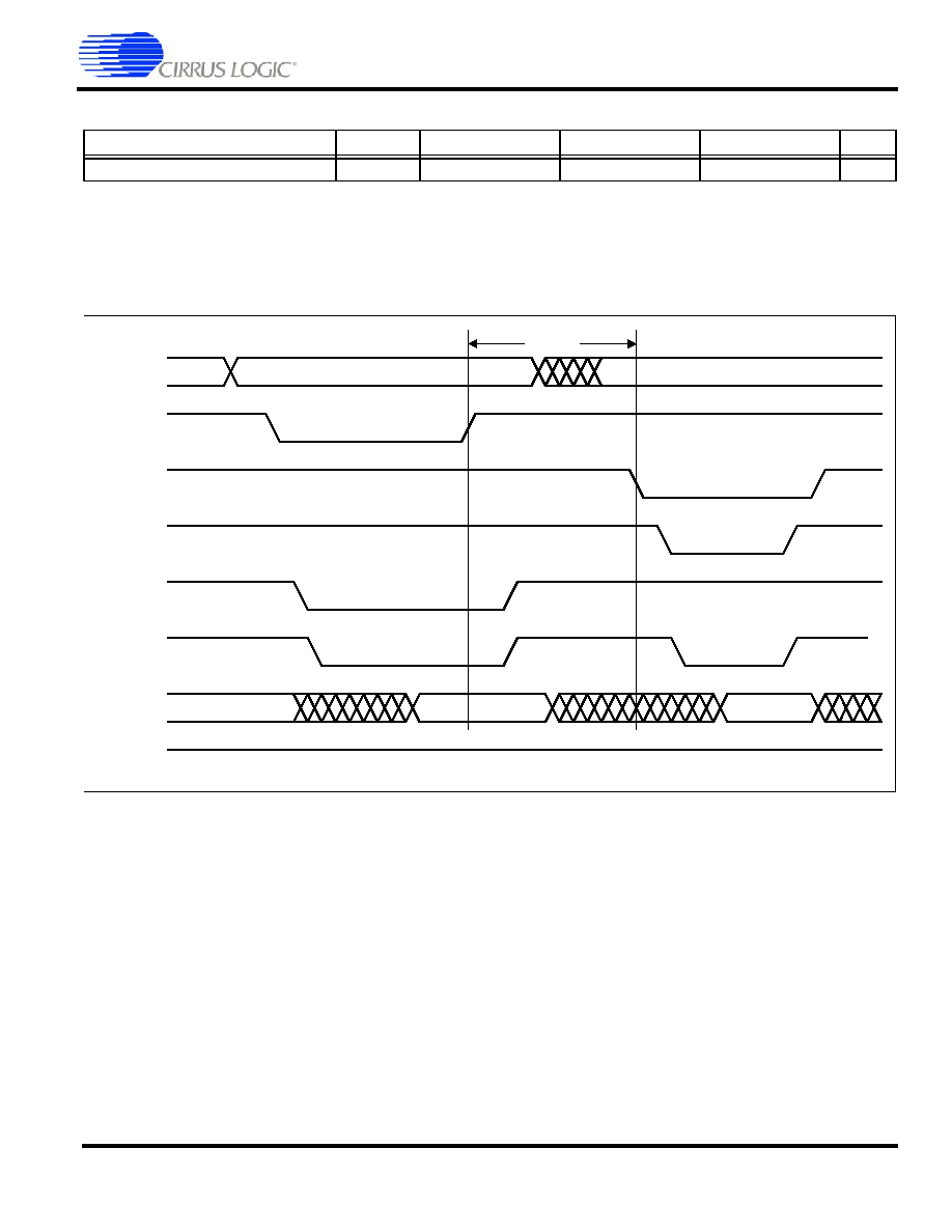
IDE Interface
Register Transfers
Note:
1. t
0
is the minimum total cycle time, t
2
is the minimum DIORn / DIOWn assertion time, and t
2i
is the minimum DIORn / DIOWn
negation time. A host implementation shall lengthen t
2
and/or t
2i
to ensure that t
0
is equal to or greater than the value
reported in the devices IDENTIFY DEVICE data. A device implementation shall support any legal host implementation.
2. This parameter specifies the time from the negation edge of DIORn to the time that the data bus is released by the device.
3. The delay from the activation of DIORn or DIOWn until the state of IORDY is first sampled. If IORDY is inactive then the host
shall wait until IORDY is active before the register transfer cycle is completed. If the device is not driving IORDY negated at
the t
A
after the activation of DIORn or DIOWn, then t
5
shall be met and t
RD
is not applicable. If the device is driving IORDY
negated at the time t
A
after the activation of DIORn or DIOWn, then t
RD
shall be met and t
5
is not applicable.
4. Timings based upon software control. See User's Guide.
5. ATA / ATAPI standards prior to ATA / ATAPI-5 inadvertently specified an incorrect value for mode 2 time t
0
by utilizing the
16-bit PIO value.
6. All IDE timing is based upon HCLK = 100 MHz.
Parameter
Symbol
Mode 0
(in ns)
Mode 1
(in ns)
Mode 2
(in ns)
Mode 3
(in ns)
Mode 4
(in ns)
Cycle time
(min)
(Notes 1, 4, 5)
t
0
600
383
330
180
120
Address valid to DIORn / DIOWn setup
(min)
(Note 4)
t
1
70
50
30
30
25
DIORn / DIOWn pulse width 8-bit
(min)
(Note 1, 4)
t
2
290
290
290
80
70
DIORn / DIOWn recovery time
(min)
(Note 1, 4)
t
2i
-
-
-
70
25
DIOWn data setup
(min)
(Note 4)
t
3
60
45
30
30
20
DIOWn data hold
(min)
t
4
0
0
0
0
0
DIORn data setup
(min)
t
5
20
20
20
20
20
DIORn data hold
(min)
t
6
0
0
0
0
0
DIORn data high impedance state
(max)
(Note 2, 4)
t
6z
30
30
30
30
30
DIORn / DIOWn to address valid hold
(min)
(Note 4)
t
9
20
15
10
10
10
Read Data Valid to IORDY
(min)
active (if IORDY initially low after t
A
)
(Note 4)
t
RD
0
0
0
0
0
IORDY Setup time
(Note 3, 4)
t
A
35
35
35
35
35
IORDY Pulse Width
(max)
(Note 4)
t
B
1250
1250
1250
1250
1250
IORDY assertion to release
(max)
t
C
5
5
5
5
5
DIOWn assert to data valid
(max)
t
DDV
10
10
10
10
10
DS515PP7
©
Copyright 2005 Cirrus Logic (All Rights Reserved)
31
EP9312
Universal Platform SOC Processor
Note:
1. Device address consists of signals IDECS0n, IDECS1n and IDEDA (2:0)
2. Data consists of DD (7:0)
3. The negation of IORDY by the device is used to extend the register transfer cycle. The determination of whether the cycle is
to be extended is made by the host after t
A
from the assertion of DIORn or DIOWn. The assertion and negation or IORDY
are described in the following three cases:
3-1 Device never negates IORDY, devices keeps IORDY released: no wait is generated.
3-2 Device negates IORDY before t
A
, but causes IORDY to be asserted before t
A
. IORDY is released prior to negation
and may be asserted for no more than t
C
before release: no wait generated.
3-3 Device negates IORDY before t
A
. IORDY is released prior to negation and may be asserted for no more than t
C
before release: wait generated. The cycle completes after IORDY is reasserted. For cycles where a wait is generated
and DIORn is asserted, the device shall place read data on DD (7:0) for t
RD
before asserting IORDY.
Figure 17. Register Transfer to/from Device
ADDR valid
(Note 1)
DIORn/
DIOWn
WRITE
DD (7:0)
(Note 2)
READ
DD (7:0)
(Note 2)
IORDY
(Note 3,3-1)
IORDY
(Note 3,3-2)
IORDY
(Note 3,3-3)
t
0
t
1
t
2
t
9
t
2i
t
3
t
4
t
5
t
6
t
6z
t
A
t
B
t
C
t
C
t
RD
t
DDV
32
©
Copyright 2005 Cirrus Logic (All Rights Reserved)
DS515PP7
EP9312
Universal Platform SOC Processor
PIO Data Transfers
Note:
1. t
0
is the minimum total cycle time, t
2
is the minimum DIORn / DIOWn assertion time, and t
2i
is the minimum DIORn / DIOWn
negation time. A host implementation shall lengthen t
2
and/or t
2i
to ensure that t
0
is equal to or greater than the value
reported in the devices IDENTIFY DEVICE data. A device implementation shall support any legal host implementation.
2. This parameter specifies the time from the negation edge of DIORn to the time that the data bus is released by the device.
3. The delay from the activation of DIORn or DIOWn until the state of IORDY is first sampled. If IORDY is inactive then the host
shall wait until IORDY is active before the register transfer cycle is completed. If the device is not driving IORDY negated at
the t
A
after the activation of DIORn or DIOWn, then t
5
shall be met and t
RD
is not applicable. If the device is driving IORDY
negated at the time t
A
after the activation of DIORn or DIOWn, then t
RD
shall be met and t
5
is not applicable.
4. Timings based upon software control. See User's Guide.
5. All IDE timing is based upon HCLK = 100 MHz.
Parameter
Symbol
Mode 0
(in ns)
Mode 1
(in ns)
Mode 2
(in ns)
Mode 3
(in ns)
Mode 4
(in ns)
Cycle time
(min)
(Note 1, 4)
t
0
600
383
240
180
120
Address valid to DIORn / DIOWn setup
(min)
(Note 4)
t
1
70
50
30
30
25
DIORn / DIOWn 16-bit
(min)
(Note 1, 4)
t
2
165
125
100
80
70
DIORn / DIOWn recovery time
(min)
(Note 1, 4)
t
2i
-
-
-
70
25
DIOWn data setup
(min)
(Note 4)
t
3
60
45
30
30
20
DIOWn data hold
(min)
t
4
0
0
0
0
0
DIORn data setup
(min)
t
5
20
20
20
20
20
DIORn data hold
(min)
t
6
0
0
0
0
0
DIORn data high impedance state
(max)
(Note 2, 4)
t
6z
30
30
30
30
30
DIORn / DIOWn to address valid hold
(min)
(Note 4)
t
9
20
15
10
10
10
Read Data Valid to IORDY
(min)
active (if IORDY initially low after t
A
)
(Note 4)
t
RD
0
0
0
0
0
IORDY Setup time
(Note 3, 4)
t
A
35
35
35
35
35
IORDY Pulse Width
(max)
(Note 4)
t
B
1250
1250
1250
1250
1250
IORDY assertion to release
(max)
t
C
5
5
5
5
5
DIOWn assert to data valid
(max)
t
DDV
10
10
10
10
10

DS515PP7
©
Copyright 2005 Cirrus Logic (All Rights Reserved)
33
EP9312
Universal Platform SOC Processor
Note:
1. Device address consists of signals IDECS0n, IDECS1n and IDEDA (2:0)
2. Data consists of DD (15:0)
3. The negation of IORDY by the device is used to extend the register transfer cycle. The determination of whether the cycle is
to be extended is made by the host after t
A
from the assertion of DIORn or DIOWn. The assertion and negation or IORDY
are described in the following three cases:
3-1 Device never negates IORDY, devices keeps IORDY released: no wait is generated.
3-2 Device negates IORDY before t
A
, but causes IORDY to be asserted before t
A
. IORDY is released prior to negation
and may be asserted for no more than t
C
before release: no wait generated.
3-3 Device negates IORDY before t
A
. IORDY is released prior to negation and may be asserted for no more than t
C
before release: wait generated. The cycle completes after IORDY is reasserted. For cycles where a wait is generated
and DIORn is asserted, the device shall place read data on DD (15:0) for t
RD
before asserting IORDY.
Figure 18. PIO Data Transfer to/from Device
ADDR valid
(Note 1)
DIORn/
DIOWn
WRITE
DD(15:0)
(Note 2)
READ
DD(15:0)
(Note 2)
IORDY
(Note 3,3-1)
IORDY
(Note 3,3-2)
IORDY
(Note 3,3-3)
t
0
t
1
t
2
t
9
t
2i
t
3
t
4
t
5
t
6
t
6z
t
A
t
B
t
C
t
C
t
RD
t
DDV

34
©
Copyright 2005 Cirrus Logic (All Rights Reserved)
DS515PP7
EP9312
Universal Platform SOC Processor
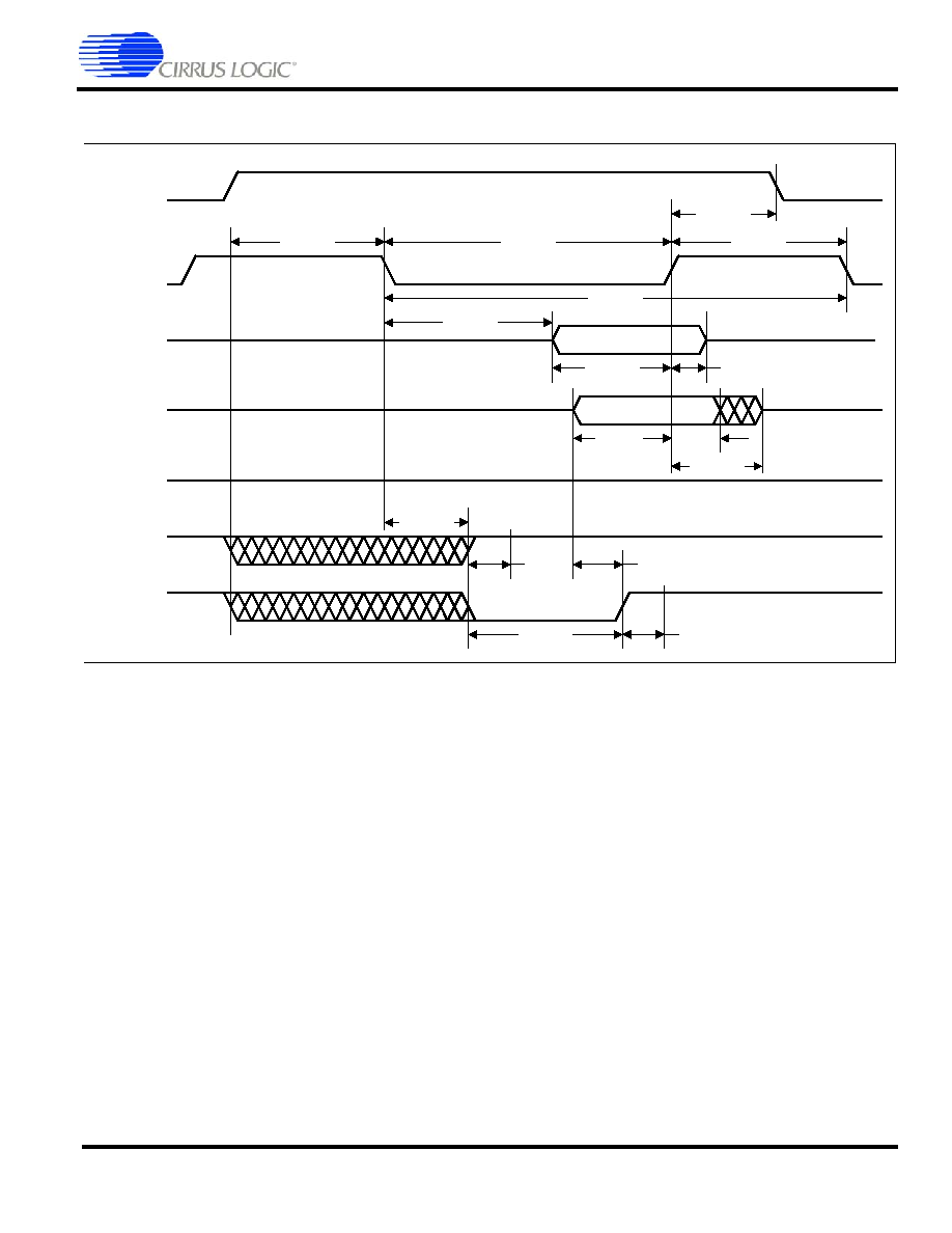
Ultra DMA Data Transfer
Figure 19
through
Figure 28
define the timings associated with all phases of Ultra DMA bursts. The following table
contains the values for the timings for each of the Ultra DMA modes.
Note:
1. Timing parameters shall be measured at the connector of the sender or receiver to which the parameter applies.
2. The test load for t
DVS
and t
DVH
shall be a lumped capacitor load with no cable or receivers. Timing for t
DVS
and t
DVH
shall be
met for all capacitive loads from 15 to 40 pf where all signals have the same capacitive load value.
3. t
UI
, t
MLI
and t
LI
indicate sender-to-recipient or recipient-to-sender interlocks, i.e., either sender or recipient is waiting for the
other to respond with a signal before proceeding. t
UI
is an unlimited interlock that has no maximum time value. t
MLI
is a limited
time-out that has a defined minimum. t
LI
is a limited time-out that has a defined maximum.
4. t
ZIORDY
may be greater than t
ENV
since the device has a pull up on IORDYn giving it a known state when released.
5. All IDE timing is based upon HCLK = 100 MHz.
Timing reference levels = 1.5 V
Parameter
Symbol
Mode 0
(in ns)
Mode 1
(in ns)
Mode 2
(in ns)
Mode 3
(in ns)
min max min max min max min max
Cycle time allowing for asymmetry and clock variations
(from DSTROBE edge to DSTROBE edge)
t
CYCRD
112
-
73
-
54
-
39
-
Two-cycle time allowing for clock variations (from rising edge to next
rising edge or from falling edge to next falling edge of DSTROBE)
t
2CYCRD
230
-
154
-
115
-
86
-
Cycle time allowing for asymmetry and clock variations
(from HSTROBE edge to HSTROBE edge)
t
CYCWR
230
-
170
-
130
-
100
-
Two-cycle time allowing for clock variations (from rising edge to next
rising edge or from falling edge to next falling edge of HSTROBE)
t
2CYCWR
460
-
340
-
260
-
200
-
Data setup time at recipient (Read)
t
DS
15
-
10
-
7
-
7
-
Data hold time at recipient (Read)
t
DH
8
-
8
-
8
-
8
-
Data valid setup time at sender (Write)
(Note 2)
(from data valid until STROBE edge)
t
DVS
70
-
48
-
30
-
20
-
Data valid hold time at sender (Write)
(Note 2)
(from STROBE edge until data may become invalid)
t
DVH
6
-
6
-
6
-
6
-
First STROBE time (for device to first negate DSTROBE from STOP
during a data in burst)
t
FS
0
230
0
200
0
170
0
130
Limited interlock time
(Note 3)
t
LI
0
150
0
150
0
150
0
100
Interlock time with minimum
(Note 3)
t
MLI
20
-
20
-
20
-
20
-
Unlimited interlock time
(Note 3)
t
UI
0
-
0
-
0
-
0
-
Maximum time allowed for output drivers to release
(from asserted or negated)
t
AZ
-
10
-
10
-
10
-
10
Minimum delay time required for output
t
ZAH
20
-
20
-
20
-
20
-
Drivers to assert or negate (from released)
t
ZAD
0
-
0
-
0
-
0
-
Envelope time (from DMACKn to STOP and HDMARDYn during data in
burst initiation and from DMACKn to STOP during data out burst initiation)
t
ENV
20
70
20
70
20
70
20
55
Ready-to-final-STROBE time (no STROBE edges shall be sent this long
after negation of DMARDYn)
t
RFS
-
75
-
70
-
60
-
60
Ready-to-pause time
(that recipient shall wait to pause after negating DMARDYn)
t
RP
160
-
125
-
100
-
100
-
Maximum time before releasing IORDY
t
IORDYZ
-
20
-
20
-
20
-
20
Minimum time before driving STROBE
(Note 4)
t
ZIORDY
0
-
0
-
0
-
0
-
Setup and hold times for DMACKn (before assertion or negation)
t
ACK
20
-
20
-
20
-
20
-
Time from STROBE edge to negation of DMARQ or assertion of STOP
(when sender terminates a burst)
t
SS
50
-
50
-
50
-
50
-
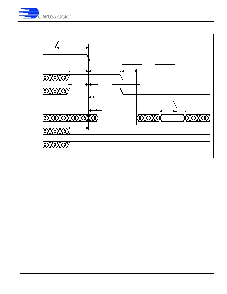
DS515PP7
©
Copyright 2005 Cirrus Logic (All Rights Reserved)
35
EP9312
Universal Platform SOC Processor
Note:
The definitions for the DIOWn:STOP, DIORn:HDMARDYn:HSTROBE and IORDY:DDMARDYn:DSTROBE signal lines are not
in effect until DMARQ and DMACKn are asserted.
Figure 19. Initiating an Ultra DMA data-in Burst
DMARQ
(device)
DMACKn
(host)
STOP
(host)
HDMARDYn
(host)
DSTROBE
(device)
DD (15:0)
IDEDA[2:0]
IDECS0n,
IDECS1n
t
UI
t
ACK
t
ACK
t
ACK
t
AZ
t
ZIORDY
t
ENV
t
ZAD
t
DVS
t
DVH
t
FS
t
ZAD
t
ENV
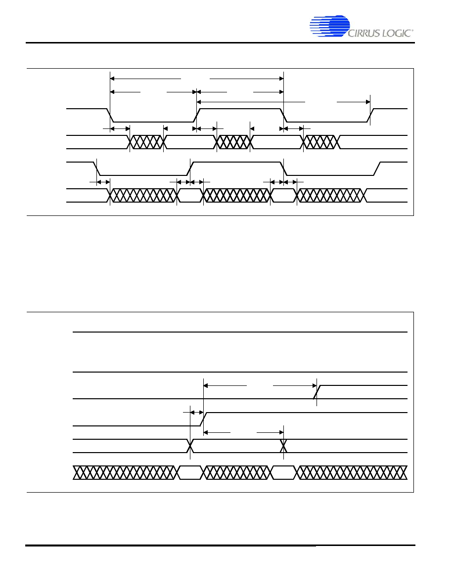
36
©
Copyright 2005 Cirrus Logic (All Rights Reserved)
DS515PP7
EP9312
Universal Platform SOC Processor
Note:
DD (15:0) and DSTROBE signals are shown at both the host and the device to emphasize that cable settling time as well as
cable propagation delay shall not allow the data signals to be considered stable at the host until some time after they are driven
by the device.
Figure 20. Sustained Ultra DMA data-in Burst
Figure 21. Host Pausing an Ultra DMA data-in Burst
DSTROBE
(device)
DD (15:0)
(device)
DSTROBE
(host)
DD (15:0)
(host)
t
CYCRD
t
2CYCRD
t
2CYCRD
t
CYCRD
t
DVH
t
DVS
t
DVH
t
DVS
t
DVH
t
DH
t
DS
t
DS
t
DH
t
DH
DD(15:0)
(device)
DSTROBE
(device)
HDMARDYn
(host)
STOP
(host)
DMACKn
(host)
DMARQ
(device)
t
RP
t
SR
t
RFS
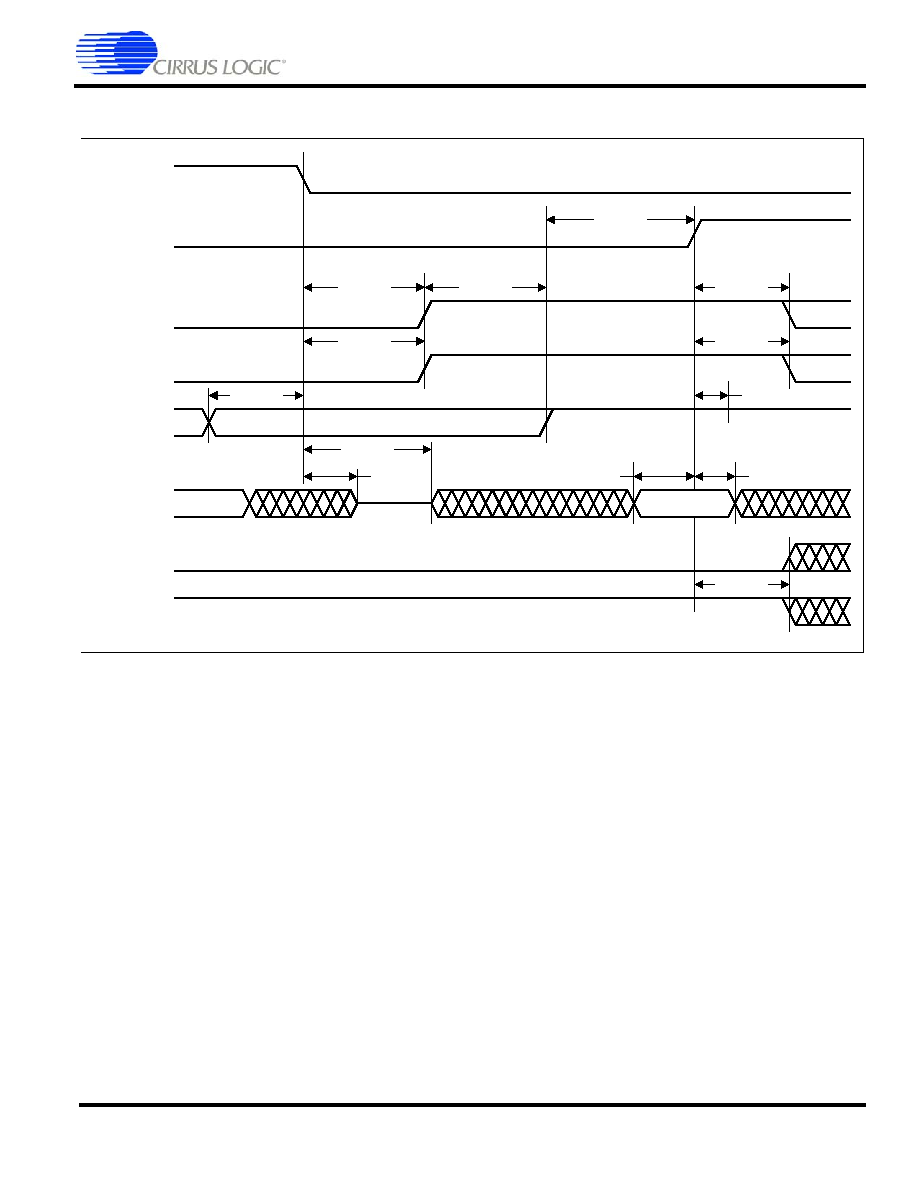
DS515PP7
©
Copyright 2005 Cirrus Logic (All Rights Reserved)
37
EP9312
Universal Platform SOC Processor
Note:
The definitions for the DIOWn:STOP, DIORn:HDMARDYn:HSTROBE and IORDY:DDMARDYn:DSTROBE signal lines are no
longer in effect after DMARQ and DMACKn are negated.
Figure 22. Device Terminating an Ultra DMA data-in Burst
DMARQ
(device)
DMACKn
(host)
STOP
(host)
HDMARDYn
(host)
DSTROBE
(device)
DD (15:0)
IDEDA[2:0]
IDECS0n,
IDECS1n
t
LI
t
MLI
t
ZAH
t
ACK
t
SS
t
AZ
t
DVS
t
DVH
t
IORDYZ
t
LI
t
LI
t
ACK
t
ACK
CRC
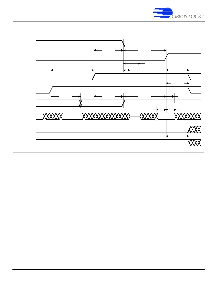
38
©
Copyright 2005 Cirrus Logic (All Rights Reserved)
DS515PP7
EP9312
Universal Platform SOC Processor
Note:
The definitions for the DIOWn:STOP, DIORn:HDMARDYn:HSTROBE and IORDY:DDMARDYn:DSTROBE signal lines are no
longer in effect after DMARQ and DMACKn are negated.
Figure 23. Host Terminating an Ultra DMA data-in Burst
DMARQ
(device)
DMACKn
(host)
STOP
(host)
HDMARDYn
(host)
DSTROBE
(device)
DD (15:0)
IDEDA[2:0]
IDECS0n,
IDECS1n
t
LI
t
LI
t
RP
t
RFS
t
MLI
t
ACK
t
ACK
t
ACK
t
DVH
t
DVS
t
MLI
t
ZAH
t
AZ
t
IORDYZ
CRC

DS515PP7
©
Copyright 2005 Cirrus Logic (All Rights Reserved)
39
EP9312
Universal Platform SOC Processor
Note:
The definitions for the DIOWn:STOP, DIORn:HDMARDYn:HSTROBE and IORDY:DDMARDYn:DSTROBE signal lines are not
in effect until DMARQ and DMACKn are asserted.
Figure 24. Initiating an Ultra DMA data-out Burst
DMARQ
(device)
DMACKn
(host)
STOP
(host)
DDMARDYn
(device)
HSTROBE
(host)
DD (15:0)
IDEDA[2:0]
IDECS0n,
IDECS1n
t
UI
t
ACK
t
ACK
t
ACK
t
ENV
t
LI
t
UI
t
DVS
t
DVH
t
ZIORDY
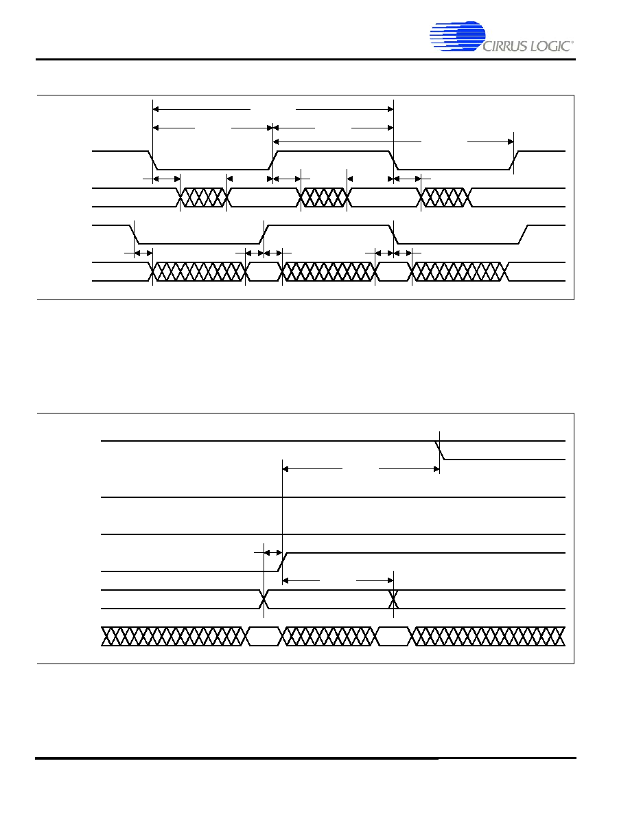
40
©
Copyright 2005 Cirrus Logic (All Rights Reserved)
DS515PP7
EP9312
Universal Platform SOC Processor
Note:
DD (15:0) and HSTROBE signals are shown at both the device and the host to emphasize that cable settling time as well as
cable propagation delay shall not allow the data signals to be considered stable at the device until some time after they are
driven by the host.
Figure 25. Sustained Ultra DMA data-out Burst
Note:
1. The device may negate DMARQ to request termination of the Ultra DMA burst no sooner than t
RP
after DDMARDYn is
negated.
2. If the t
SR
timing is not satisfied, the device may receive zero, one, or two more data words from the host.
Figure 26. Device Pausing an Ultra DMA data-out Burst
HSTROBE
(host)
DD (15:0)
(host)
HSTROBE
(device)
DD (15:0)
(device)
t
CYCWR
t
2CYCWR
t
2CYCWR
t
CYCWR
t
DVH
t
DVS
t
DVH
t
DVS
t
DVH
t
DH
t
DS
t
DS
t
DH
t
DH
DD (15:0)
(host)
HSTROBE
(host)
DDMARDYn
(device)
STOP
(host)
DMACKn
(host)
DMARQ
(device)
t
RP
t
SR
t
RFS
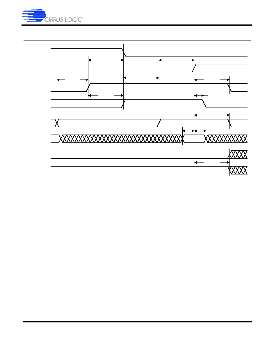
DS515PP7
©
Copyright 2005 Cirrus Logic (All Rights Reserved)
41
EP9312
Universal Platform SOC Processor
Note:
The definitions for the DIOWn:STOP, IORDY:DDMARDYn:DSTROBE and DIORn:HDMARDYn:HSTROBE signal lines are no
longer in effect after DMARQ and DMACKn are negated.
Figure 27. Host Terminating an Ultra DMA data-out Burst
DMARQ
(device)
DMACKn
(host)
STOP
(host)
DDMARDYn
(device)
HSTROBE
(host)
DD (15:0)
(host)
IDEDA[2:0]
IDECS0n,
IDECS1n
t
DVH
t
DVS
t
LI
t
LI
t
LI
t
MLI
t
SS
t
ACK
t
ACK
t
ACK
t
IORDYZ
CRC
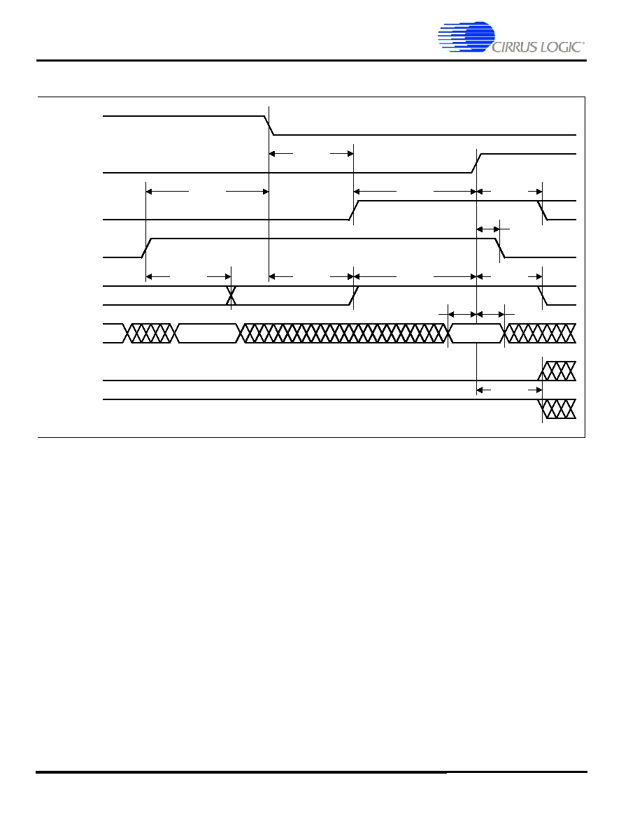
42
©
Copyright 2005 Cirrus Logic (All Rights Reserved)
DS515PP7
EP9312
Universal Platform SOC Processor
Note:
The definitions for the DIOWn:STOP, IORDY:DDMARDYn:DSTROBE and DIORn:HDMARDYn:HSTROBE signal lines are no
longer in effect after DMARQ and DMACKn are negated.
Figure 28. Device Terminating an Ultra DMA data-out Burst
DMARQ
(device)
DMACKn
(host)
STOP
(host)
DDMARDYn
(device)
HSTROBE
(host)
DD (15:0)
(host)
IDEDA[2:0]
IDECS0n,
IDECS1n
t
LI
t
LI
t
RP
t
RFS
t
MLI
t
ACK
t
ACK
t
ACK
t
DVH
t
DVS
t
MLI
t
IORDYZ
CRC
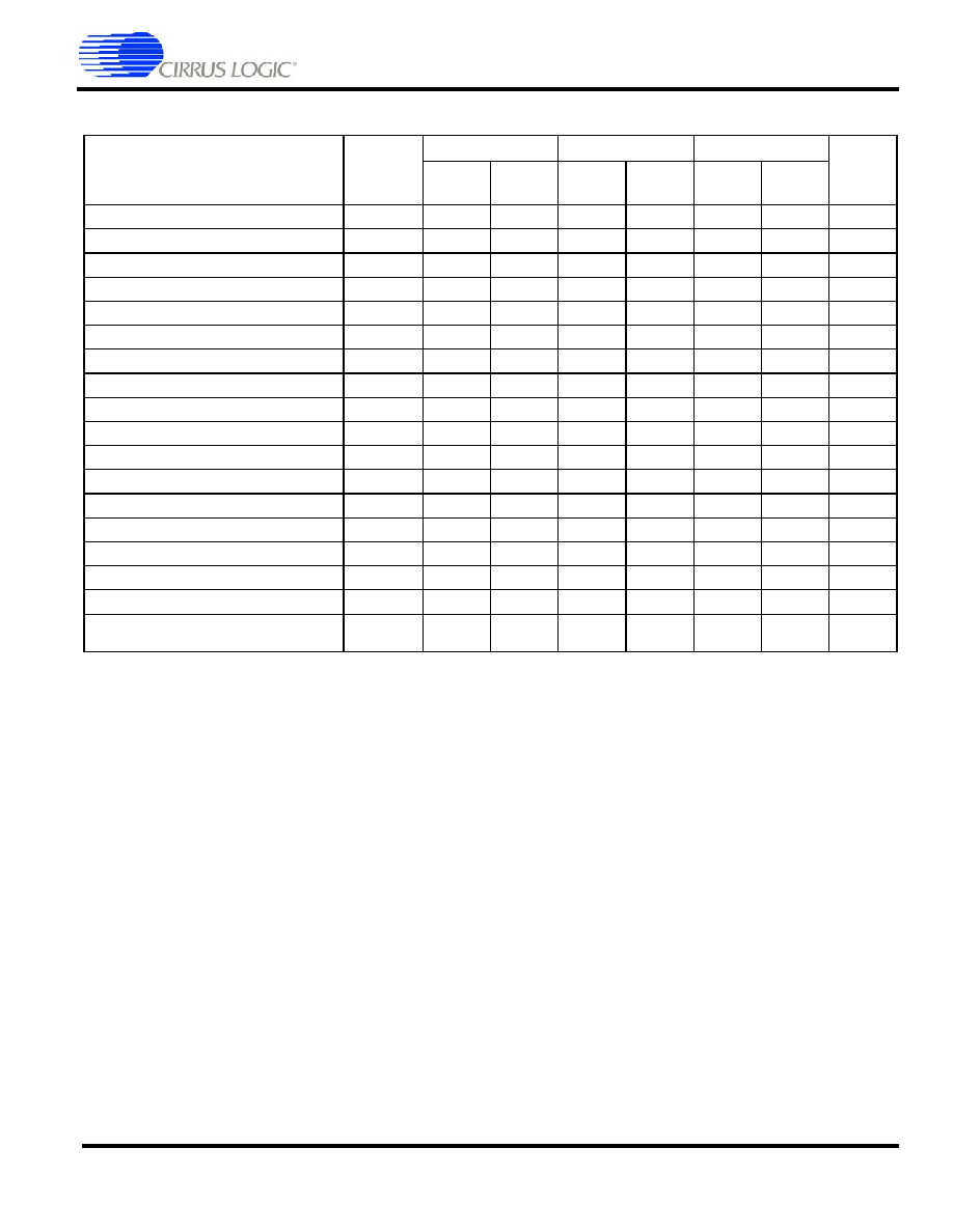
DS515PP7
©
Copyright 2005 Cirrus Logic (All Rights Reserved)
43
EP9312
Universal Platform SOC Processor
Ethernet MAC Interface
STA - Station - Any device that contains an IEEE 802.11 conforming Medium Access Control (MAC) and physical layer
(PHY) interface to the wireless medium.
PHY - Ethernet physical layer interface.
Parameter
Symbol
Min
Typ
Max
Unit
10 Mbit
mode
100 Mbit
mode
10 Mbit
mode
100 Mbit
mode
10 Mbit
mode
100 Mbit
mode
TXCLK cycle time
t
TX_per
-
-
400
40
-
-
ns
TXCLK high time
t
TX_high
140
14
200
20
260
26
ns
TXCLK low time
t
TX_low
140
14
200
20
260
26
ns
TXCLK to signal transition delay time
t
TXd
0
0
10
10
25
25
ns
TXCLK rise/fall time
t
TXrf
-
-
-
-
5
5
ns
RXCLK cycle time
t
RX_per
-
-
400
40
-
-
ns
RXCLK high time
t
RX_high
140
14
200
20
260
26
ns
RXCLK low time
t
RX_low
140
14
200
20
260
26
ns
RXDVAL / RXERR setup time
t
RXs
10
10
-
-
-
-
ns
RXDVAL / RXERR hold time
t
RXh
10
10
-
-
-
-
ns
RXCLK rise/fall time
t
RXrf
-
-
-
-
5
5
ns
MDC cycle time
t
MDC_per
-
-
400
400
-
-
ns
MDC high time
t
MDC_high
160
160
-
-
-
-
ns
MDC low time
t
MDC_low
160
160
-
-
-
-
ns
MDC rise/fall time
t
MDCrf
-
-
-
-
5
5
ns
MDIO setup time (STA sourced)
t
MDIOs
10
10
-
-
-
-
ns
MDIO hold time (STA sourced)
t
MDIOh
10
10
-
-
-
-
ns
MDC to MDIO signal transition delay time
(PHY sourced)
t
MDIOd
-
-
-
-
300
300
ns
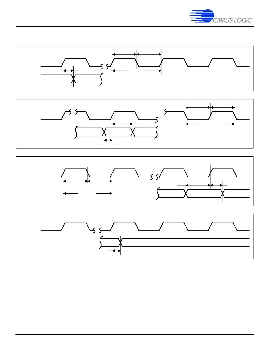
44
©
Copyright 2005 Cirrus Logic (All Rights Reserved)
DS515PP7
EP9312
Universal Platform SOC Processor
Figure 29. Ethernet MAC Timing Measurement
TXCLK
TXD[3:0]/
TXEN/
TXERR
RXCLK
RXD[3:0]/
RXDVAL/
RXERR
MDC
MDIO
(Sourced
by STA)
MDC
MDIO
(Sourced
by PHY)
t
TXd
t
RXs
t
RXh
t
MDIOs
t
MDIOh
t
TX_high
t
TX_low
t
RX_high
t
RX_low
t
MDC_high
t
MDC_low
t
TX_per
t
RX_per
t
MDC_per
t
MDIOd

DS515PP7
©
Copyright 2005 Cirrus Logic (All Rights Reserved)
45
EP9312
Universal Platform SOC Processor
Audio Interface
Note:
The tspix_clk is programmable by the user.
The following table contains the values for the timings of each of the SPI modes.
Parameter
Symbol
Min
Typ
Max
Unit
SCLK cycle time
t
clk_per
-
tspix_clk
-
ns
SCLK high time
t
clk_high
-
(tspix_clk) / 2
-
ns
SCLK low time
t
clk_low
-
(tspix_clk) / 2
-
ns
SCLK rise/fall time
t
clkrf
1
-
8
ns
Data from master valid delay time
t
DMd
-
-
3
ns
Data from master setup time
t
DMs
20
-
-
ns
Data from master hold time
t
DMh
40
-
-
ns
Data from slave setup time
t
DSs
20
-
-
ns
Data from slave hold time
t
DSh
40
-
-
ns
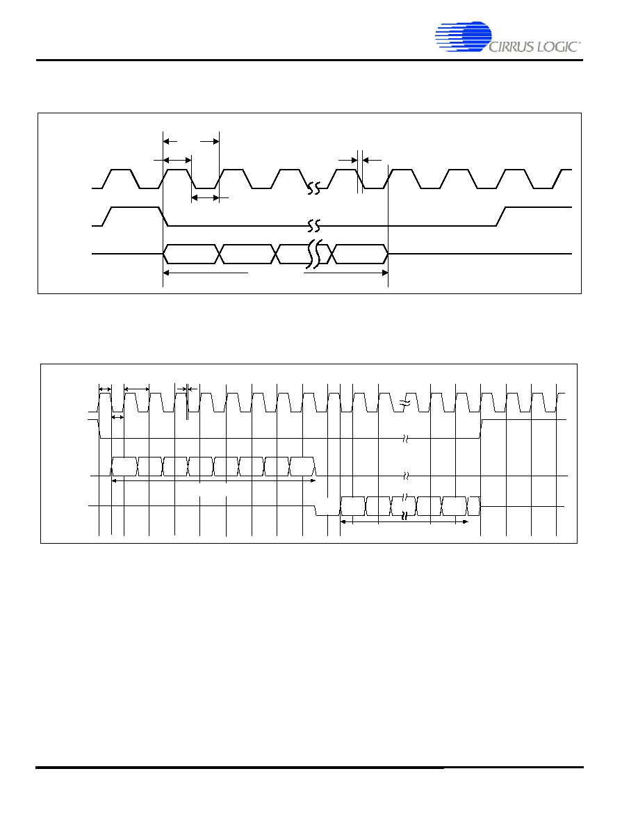
46
©
Copyright 2005 Cirrus Logic (All Rights Reserved)
DS515PP7
EP9312
Universal Platform SOC Processor
Texas Instruments' Synchronous Serial Format
Microwire
Figure 30. TI Single Transfer Timing Measurement
Figure 31. Microwire Frame Format, Single Transfer
SCLK
SFRM
SSPTXD/
SSPRXD
4 to 16 bits
MSB
LSB
t
clk_per
t
clk_low
t
clk_high
t
clkrf
SCLK
SFRM
SSPTXD
SSPRXD
0
MSB
LSB
4 to 16 bits output data
t
clkrf
t
clk_high
t
clk_low
t
clk_per
MSB
LSB
8-bit control
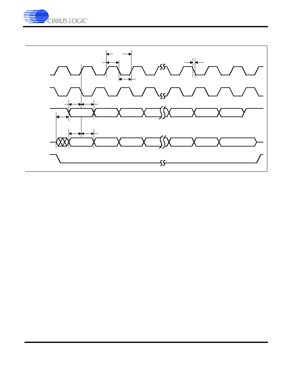
DS515PP7
©
Copyright 2005 Cirrus Logic (All Rights Reserved)
47
EP9312
Universal Platform SOC Processor
Motorola SPI
Figure 32. SPI Format with SPH=1 Timing Measurement
SCLK
(SPO=0)
SCLK
(SPO=1)
SSPTXD
(master)
SSPRXD
(slave)
SFRM
MSB
LSB
LSB
MSB
t
clk_per
t
clk_low
t
clk_high
t
clkrf
t
DMd
t
DMs
t
DMh
t
DSs
t
DSh
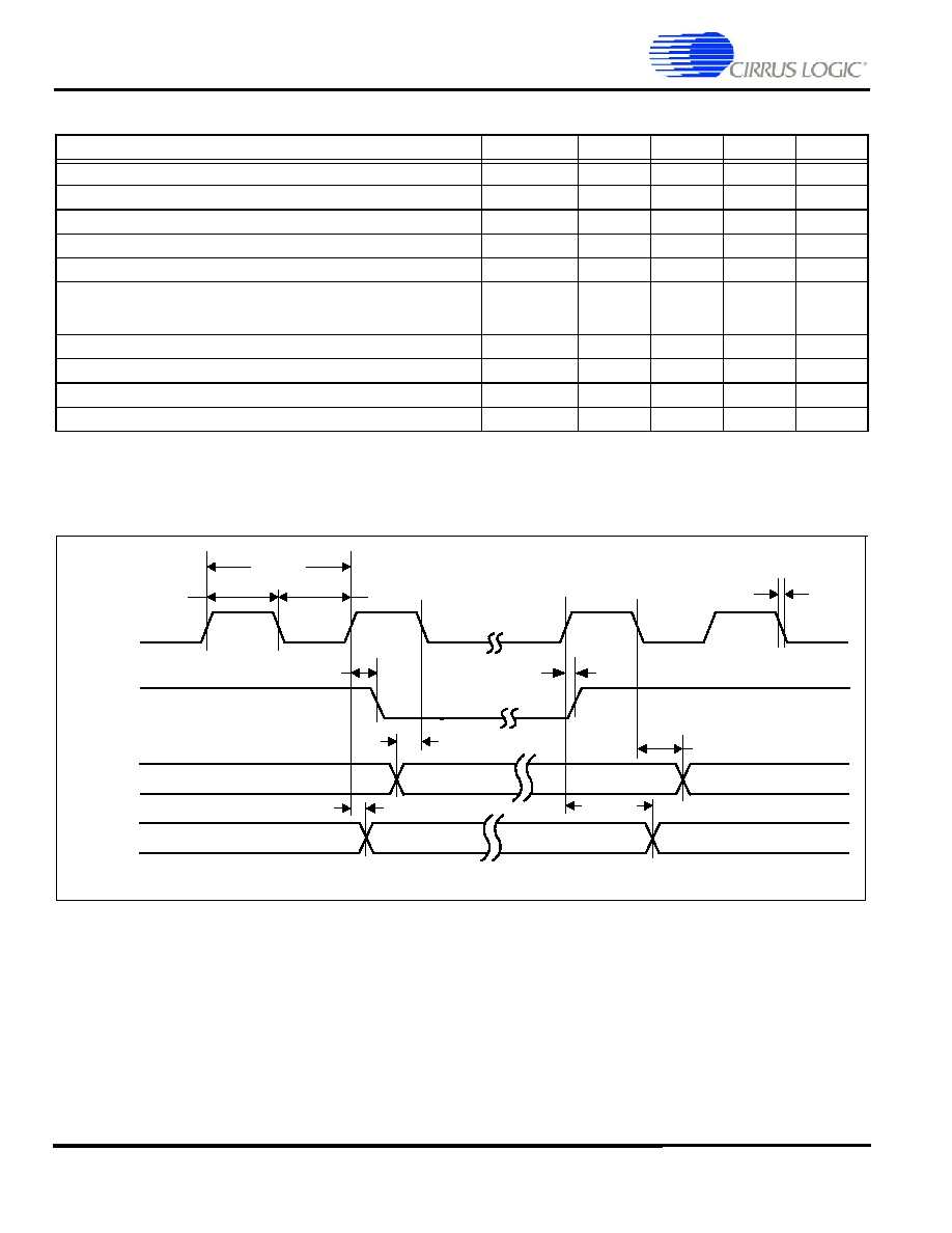
48
©
Copyright 2005 Cirrus Logic (All Rights Reserved)
DS515PP7
EP9312
Universal Platform SOC Processor
Inter-IC Sound - I
2
S
Note:
t
i2s_clk
is programmable by the user.
Parameter
Symbol
Min
Typ
Max
Unit
SCLK cycle time
t
clk_per
-
t
i2s_clk
-
ns
SCLK high time
t
clk_high
-
(t
i2s_clk
) / 2
-
ns
SCLK low time
t
clk_low
-
(t
i2s_clk
) / 2
-
ns
SCLK rise/fall time
t
clkrf
1
4
8
ns
SCLK to LRCLK assert delay time
t
LRd
-
-
3
ns
Hold between SCLK assert then LRCLK deassert
or
Hold between LRCLK deassert then SCLK assert
t
LRh
0
-
-
ns
SDI to SCLK deassert setup time
t
SDIs
12
-
-
ns
SDI from SCLK deassert hold time
t
SDIh
0
-
-
ns
SCLK assert to SDO delay time
t
SDOd
-
-
9
ns
SDO from SCLK assert hold time
t
SDOh
1
-
-
ns
Figure 33. Inter-IC Sound (I
2
S) Timing Measurement
SCLK
LRCLK
SDI
t
LRd
t
LRh
t
SDIh
t
clk_high
t
SDIs
t
clk_low
t
clk_per
t
clkrf
t
SDOh
SDO
t
SDOd
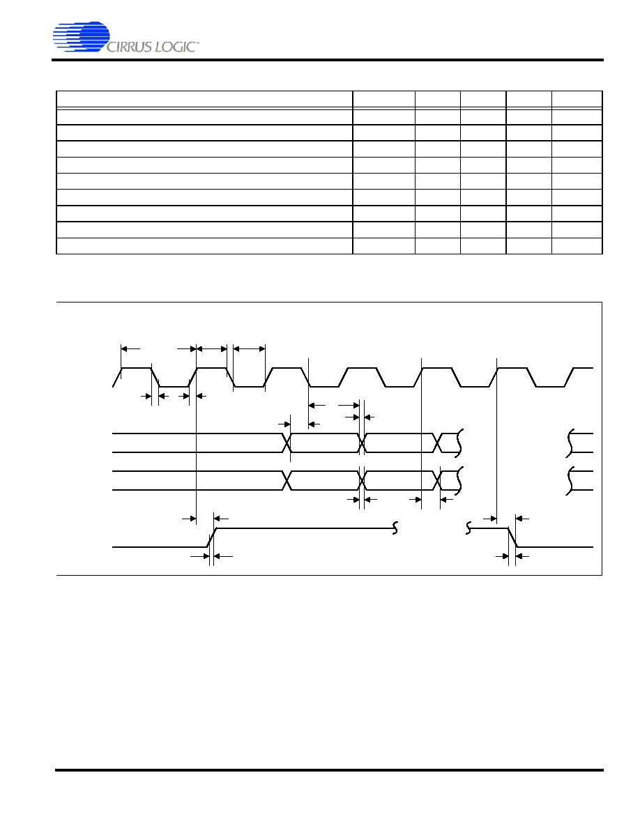
DS515PP7
©
Copyright 2005 Cirrus Logic (All Rights Reserved)
49
EP9312
Universal Platform SOC Processor
AC'97
Parameter
Symbol
Min
Typ
Max
Unit
ABITCLK input cycle time
t
clk_per
-
81.4
-
ns
ABITCLK input high time
t
clk_high
36
-
45
ns
ABITCLK input low time
t
clk_low
36
-
45
ns
ABITCLK input rise/fall time
t
clkrf
2
-
6
ns
ASDI setup to ABITCLK falling
t
s
10
-
-
ns
ASDI hold after ABITCLK falling
t
h
10
-
-
ns
ASDI input rise/fall time
t
rfin
2
-
6
ns
ABITCLK rising to ASDO / ASYNC valid, C
L
= 55 pF
t
co
2
-
15
ns
ASYNC / ASDO rise/fall time, C
L
= 55 pF
t
rfout
2
-
6
ns
Figure 34. AC `97 Configuration Timing Measurement
ABITCLK
ASDI
ASDO
ASYNC
t
co
t
rfout
t
rfout
t
s
t
rfin
t
co
t
rfout
t
co
t
clkrf
t
clk_high
t
clk_low
t
h
t
clk_per
t
clkrf

50
©
Copyright 2005 Cirrus Logic (All Rights Reserved)
DS515PP7
EP9312
Universal Platform SOC Processor
LCD Interface
Parameter
Symbol
Min
Typ
Max
Unit
SPCLK rise/fall time
t
clkr
2
-
8
ns
SPCLK rising edge to control signal transition time
t
CD
-
-
3
ns
SPCLK rising edge to data transition time
t
DD
-
-
10
ns
Data valid time
t
Dv
t
SPCLK
-
-
ns
Figure 35. LCD Timing Measurement
SPCLK
HSYNC/
V_CSYNC/
BLANK/
BRIGHT
P [17:0]
t
clkrf
t
Dv
t
CD
t
DD
t
clkrf
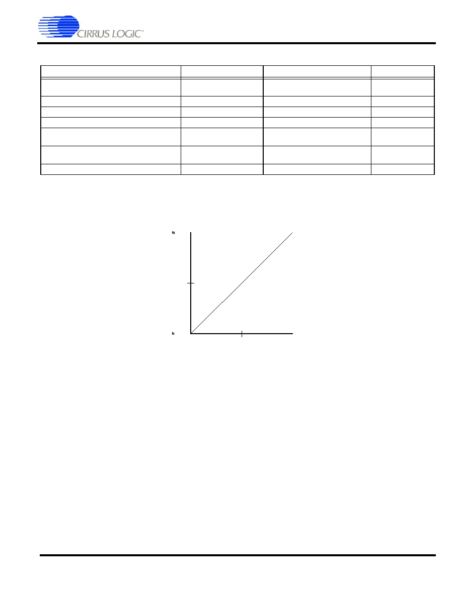
DS515PP7
©
Copyright 2005 Cirrus Logic (All Rights Reserved)
51
EP9312
Universal Platform SOC Processor
ADC
Note:
ADIV refers to bit 16 in the KeyTchClkDiv register.
ADIV = 0 means the input clock to the ADC module is equal to the external 14.7456 MHz clock divided by 4.
ADIV = 1 means the input clock to the ADC module is equal to the external 14.7456 MHz clock divided by 16.
Using the ADC:
This ADC has a state-machine based conversion engine that automates the conversion process. The initiator for a
conversion is the read access of the TSXYResult register by the CPU. The data returned from reading this register
contains the result as well as the status bit indicating the state of the ADC. However, this peripheral requires a delay
between each successful conversion and the issue of the next conversion command, or else the returned value of
successive samples may not reflect the analog input. Since the state of the ADC state machine is returned through the
same channel used to initiate the conversion process, there must be a delay inserted after every complete conversion.
Note that reading TSXYResult during a conversion will not affect the result of the ongoing process.
The following is a recommended procedure for safely polling the ADC from software:
1. Read the TSXYResult register into a local variable to initiate a conversion.
2. If the value of bit 31 of the local variable is '0' then repeat step 1.
3. Delay long enough to meet the maximum sample rate as shown above.
4. Mask the local variable with 0xFFFF to remove extraneous data.
5. If signed mode is used, do a sign extend of the lower halfword.
6. Return the sampled value.
Parameter
Comment
Value
Units
Resolution
No missing codes
Range of 0 to 3.3 V
50K counts (approximate)
Integral non-linearity
0.01%
Offset error
±15
mV
Full scale error
0.2%
Maximum sample rate
ADIV = 0
ADIV = 1
3750
925
Samples per second
Samples per second
Channel switch settling time
ADIV = 0
ADIV = 1
500
2
µ
s
ms
Noise (RMS) - typical
120
µ
V
Figure 36. ADC Transfer Function
0
Vref/2
Vref
0000
FFFF
61A8
9E58
A/D Converter Transfer Function
(approximately ±25,000 counts)

52
©
Copyright 2005 Cirrus Logic (All Rights Reserved)
DS515PP7
EP9312
Universal Platform SOC Processor
JTAG
Parameter
Symbol
Min
Max
Units
TCK clock period
t
clk_per
100
-
ns
TCK clock high time
t
clk_high
50
-
ns
TCK clock low time
t
clk_low
50
-
ns
TMS / TDI to clock rising setup time
t
JPs
20
-
ns
Clock rising to TMS / TDI hold time
t
JPh
45
-
ns
JTAG port clock to output
t
JPco
-
30
ns
JTAG port high impedance to valid output
t
JPzx
-
30
ns
JTAG port valid output to high impedance
t
JPxz
-
30
ns
Figure 37. JTAG Timing Measurement
TDO
TCK
TDI
TMS
t
JPh
t
clk_high
t
clk_low
t
JPzx
t
JPco
t
JPxz
t
clk_per
t
JPs

DS515PP7
©
Copyright 2005 Cirrus Logic (All Rights Reserved)
53
EP9312
Universal Platform SOC Processor
352 Pin BGA Package Outline
352-Ball PBGA Diagram
Figure 38. 352 Pin PBGA Pin Diagram
DETAIL B
DETAIL A'
e
D1
E1
ÿb
-C-
A'
A2
B
c
ddd C
A
3
2
-A-
-B-
B
A
0.30
0.10
ÿ
ÿ
C
S
S
C
A1
B
D
D3
E3
E
D2
E2
(Bottom View)
(Top View)

54
©
Copyright 2005 Cirrus Logic (All Rights Reserved)
DS515PP7
EP9312
Universal Platform SOC Processor
Note:
1. Controlling Dimension: Millimeter.
2. Primary Datum C and seating plane are defined by the spherical crowns of the solder balls.
3. Dimension b is measured at the maximum solder ball diameter, parallel to Primary Datum C.
4. There shall be a minimum clearance of 0.25 mm between the edge of the solder ball and the body edge.
5. Reference Document: JEDEC MO-151, BAL-2
352 Pin BGA Pinout (Bottom View)
The following table shows the 352 pin BGA pinout. (For better understanding, compare the coordinates on the x and y
axis on
Figure 40, "352 PIN BGA PINOUT", on page 55
with
Figure 38, "352 Pin PBGA Pin Diagram", on page 53
.
∑ VDD_core is CVDD.
∑ VDD_ring is RVDD.
∑ All core and ring grounds are connected together and are labelled GND.
∑ Other special power requirements are clearly labelled (i.e. H18=ADC_VDD and H19=ADC_GND).
∑ NC means that the pin is not connected.
Table R. 352 Pin Diagram Dimensions
Symbol
dimension in mm
dimension in inches
MIN
NOM
MAX
MIN
NOM
MAX
A
2.20
2.30
2.50
0.087
0.092
0.098
A1
-
0.60
-
-
0.024
-
A2
1.12
1.17
1.22
0.044
0.046
0.048
b
-
0.75
-
-
0.030
-
c
0.51
0.56
0.61
0.020
0.022
0.024
D
26.80
27.00
27.20
1.055
1.063
1.071
D1
-
24.13
-
-
0.950
-
D2
23.80
24.00
24.20
0.937
0.945
0.953
D3
17.95
18.00
18.05
0.707
0.709
0.711
E
26.80
27.00
27.20
1.055
1.063
1.071
E1
-
24.13
-
-
0.950
-
E2
23.80
24.00
24.20
0.937
0.945
0.953
E3
17.95
18.00
18.05
0.707
0.709
0.711
e
-
1.27
-
-
0.050
-
ddd
-
-
0.15
-
-
0.006
q
30∞ TYP
30∞ TYP

DS515
PP7
©
Co
py
rig
h
t 20
0
5
Cirru
s
Lo
gi
c (All Righ
ts
Re
se
rv
ed
)
5
5
EP9312
Un
ivers
a
l Platfor
m
SOC
Figure 40. 352 PIN BGA PINOUT
1
2
3
4
5
6
7
8
9
10
11
12
13
14
15
16
17
18
19
20
Y HSYNC DD[1]
DD[12]
P[2]
AD[15] DA[6] DA[4]
AD[10
]
DA[1]
AD[8]
IDEDA[
0]
DTRN
TDO
BOOT[0] EEDAT ASDO
SFRM1 RDLED USBP[1] ABITCLK Y
W P[12]
P[9]
DD[0]
P[5]
P[3]
DA[7] DA[5]
AD[11
]
AD[9]
IDECS1
N
IDEDA[
1]
TCK
TMS
EECLK
SCLK1 GRLED
INT[3]
SLA[1]
SLA[0]
RXD[2] W
V
P[16]
P[11]
P[8]
DD[15]
DD[13] P[1]
AD[1
4]
AD[12
]
DA[2]
IDECS0
N
IDEDA[
2]
TDI
GND
ASYNC SSPTX1 INT[2]
RTSN
USBP[0] CTSN
TXD[0]
V
U AD[0]
P[15]
P[10]
P[7]
P[6]
P[4] P[0]
AD[13
]
DA[3]
DA[0]
DSRN BOOT[1]
NC
SSPRX1 INT[1]
PWMO
UT
USBM[0] RXD[1]
TXD[1]
ROW[1] U
T DA[8]
BLANK
P[13]
SPCLK
V_CSY
NC
DD[1
4]
GND
CVD
D
RVDD
GND
GND
RVDD
CVDD
GND
INT[0]
USBM[1
]
RXD[0]
TXD[2] ROW[2] ROW[4] T
R AD[2]
AD[1]
P[17]
P[14]
RVDD
RVD
D
GND
CVD
D
CVDD
GND
RVDD
RVDD
ROW[0] ROW[3]
PLL_GN
D
ROW[5] R
P AD[4]
DA[10]
DA[9] BRIGHT RVDD
RVD
D
RVDD
RVDD
XTALI
PLL_VD
D
ROW[6] ROW[7] P
N DA[13] DA[12] DA[11]
AD[3]
CVDD
CVD
D
GND
GND
GND
GND
GND
GND
GND
GND
XTALO
COL[0]
COL[1]
COL[2]
N
M AD[7]
DA[14]
AD[6]
AD[5]
CVDD
GND
GND
GND
GND
GND
GND
GND
COL[4]
COL[3]
COL[6]
CSN[0] M
L DA[18] DA[17] DA[16] DA[15]
GND
GND
GND
GND
GND
GND
GND
CVDD
COL[5]
COL[7] RSTON
PRSTN L
K AD[22] DA[20] AD[21] DA[19]
RVDD
GND
GND
GND
GND
GND
GND
CVDD
SYM
SYP
SXM
SXP
K
J DA[21]
DQMN[
0]
DQMN[
1]
DQMN[2
]
GND
GND
GND
GND
GND
GND
GND
CVDD
RTCXTA
LI
XM
YP
YM
J
H
DQMN[
3]
CASN
RASN
SDCSN[
2]
CVDD
GND
GND
GND
GND
GND
GND
RVDD
RTCXTA
LO
ADC_V
DD
ADC_G
ND
XP
H
G
SDCSN[
0]
SDCSN[
1]
SDWE
N
SDCLK
RVDD
RVD
D
RVDD
RVDD EGPIO[7]
EGPIO[
9]
EGPIO[1
0]
EGPIO[11
]
G
F
SDCSN[
3]
DA[22] DA[24] AD[25]
RVDD GND
CVD
D
CVDD
GND
GND EGPIO[2]
EGPIO[
4]
EGPIO[6
]
EGPIO[8] F
E AD[23] DA[23] DA[26] CSN[6]
GND
GND
CVD
D
CVD
D
RVDD
GND
GND
RVDD
CVDD
CVDD
GND
ASDI
DIOWN
EGPIO[
0]
EGPIO[3
]
EGPIO[5] E
D AD[24] DA[25] DD[11]
SDCLK
EN
AD[19] DD[9] DD[5]
AD[16
]
MIIRXD[
2]
MIITXD[
3]
TXEN
NC
NC
NC
EGPIO[
14]
NC
USBM[2] ARSTN DIORN EGPIO[1] D
C CSN[1] CSN[3] AD[20] DA[29]
DD[10] DD[6] DD[2] MDC
MIIRXD[
3]
TXCLK
MIITXD[
0]
NC
NC
NC
NC
NC
NC
USBP[2] IORDY DMACKN C
B CSN[2] DA[31] DA[30] DA[27]
DD[7] DD[3] WRN MDIO
MIIRXD[
1]
RXERR
MIITXD[
1]
CRS
NC
NC
NC
NC
EGPIO[1
3]
NC
WAITN
TRSTN B
A CSN[7] DA[28] AD[18]
DD[8]
DD[4]
AD[1
7]
RDN
RXCL
K
MIIRXD[
0]
RXDVA
L
MIITXD[
2]
TXERR
CLD
NC
NC
NC
EGPIO[1
2]
EGPIO[
15]
NC
NC
A
1
2
3
4
5
6
7
8
9
10
11
12
13
14
15
16
17
18
19
20
56
©
Copyright 2005 Cirrus Logic (All Rights Reserved)
DS515PP7
EP9312
Universal Platform SOC Processor
Pin List
The following Plastic Ball Grid Array (PBGA) ball assignment table is sorted in order of ball.
Ball
Signal
Ball
Signal
Ball
Signal
Ball
Signal
A1
CSN[7]
E9
RVDD
L3
DA[16]
T13
CVDD
A2
DA[28]
E10
GND
L4
DA[15]
T14
GND
A3
AD[18]
E11
GND
L5
GND
T15
INT[0]
A4
DD[8]
E12
RVDD
L8
GND
T16
USBM[1]
A5
DD[4]
E13
CVDD
L9
GND
T17
RXD[0]
A6
AD[17]
E14
CVDD
L10
GND
T18
TXD[2]
A7
RDN
E15
GND
L11
GND
T19
ROW[2]
A8
RXCLK
E16
ASDI
L12
GND
T20
ROW[4]
A9
MIIRXD[0]
E17
DIOWN
L13
GND
U1
AD[0]
A10
RXDVAL
E18
EGPIO[0]
L16
CVDD
U2
P[15]
A11
MIITXD[2]
E19
EGPIO[3]
L17
COL[5]
U3
P[10]
A12
TXERR
E20
EGPIO[5]
L18
COL[7]
U4
P[7]
A13
CLD
F1
SDCSN[3]
L19
RSTON
U5
P[6]
A14
NC
F2
DA[22]
L20
PRSTN
U6
P[4]
A15
NC
F3
DA[24]
M1
AD[7]
U7
P[0]
A16
NC
F4
AD[25]
M2
DA[14]
U8
AD[13]
A17
EGPIO[12]
F5
RVDD
M3
AD[6]
U9
DA[3]
A18
EGPIO[15]
F6
GND
M4
AD[5]
U10
DA[0]
A19
NC
F7
CVDD
M5
CVDD
U11
DSRN
A20
NC
F14
CVDD
M8
GND
U12
BOOT[1]
B1
CSN[2]
F15
GND
M9
GND
U13
NC
B2
DA[31]
F16
GND
M10
GND
U14
SSPRX1
B3
DA[30]
F17
EGPIO[2]
M11
GND
U15
INT[1]
B4
DA[27]
F18
EGPIO[4]
M12
GND
U16
PWMOUT
B5
DD[7]
F19
EGPIO[6]
M13
GND
U17
USBM[0]
B6
DD[3]
F20
EGPIO[8]
M16
GND
U18
RXD[1]
B7
WRN
G1
SDCSN[0]
M17
COL[4]
U19
TXD[1]
B8
MDIO
G2
SDCSN[1]
M18
COL[3]
U20
ROW[1]
B9
MIIRXD[1]
G3
SDWEN
M19
COL[6]
V1
P[16]
B10
RXERR
G4
SDCLK
M20
CSN[0]
V2
P[11]
B11
MIITXD[1]
G5
RVDD
N1
DA[13]
V3
P[8]
B12
CRS
G6
RVDD
N2
DA[12]
V4
DD[15]
B13
NC
G15
RVDD
N3
DA[11]
V5
DD[13]
B14
NC
G16
RVDD
N4
AD[3]
V6
P[1]
B15
NC
G17
EGPIO[7]
N5
CVDD
V7
AD[14]
B16
NC
G18
EGPIO[9]
N6
CVDD
V8
AD[12]
B17
EGPIO[13]
G19
EGPIO[10]
N8
GND
V9
DA[2]
B18
NC
G20
EGPIO[11]
N9
GND
V10
IDECS0N
B19
WAITN
H1
DQMN[3]
N10
GND
V11
IDEDA[2]
B20
TRSTN
H2
CASN
N11
GND
V12
TDI
C1
CSN[1]
H3
RASN
N12
GND
V13
GND
C2
CSN[3]
H4
SDCSN[2]
N13
GND
V14
ASYNC

DS515PP7
©
Copyright 2005 Cirrus Logic (All Rights Reserved)
57
EP9312
Universal Platform SOC Processor
C3
AD[20]
H5
CVDD
N15
GND
V15
SSPTX1
C4
DA[29]
H8
GND
N16
GND
V16
INT[2]
C5
DD[10]
H9
GND
N17
XTALO
V17
RTSN
C6
DD[6]
H10
GND
N18
COL[0]
V18
USBP[0]
C7
DD[2]
H11
GND
N19
COL[1]
V19
CTSN
C8
MDC
H12
GND
N20
COL[2]
V20
TXD[0]
C9
MIIRXD[3]
H13
GND
P1
AD[4]
W1
P[12]
C10
TXCLK
H16
RVDD
P2
DA[10]
W2
P[9]
C11
MIITXD[0]
H17
RTCXTALO
P3
DA[9]
W3
DD[0]
C12
NC
H18
ADC_VDD
P4
BRIGHT
W4
P[5]
C13
NC
H19
ADC_GND
P5
RVDD
W5
P[3]
C14
NC
H20
XP
P6
RVDD
W6
DA[7]
C15
NC
J1
DA[21]
P15
RVDD
W7
DA[5]
C16
NC
J2
DQMN[0]
P16
RVDD
W8
AD[11]
C17
NC
J3
DQMN[1]
P17
XTALI
W9
AD[9]
C18
USBP[2]
J4
DQMN[2]
P18
PLL_VDD
W10
IDECS1N
C19
IORDY
J5
GND
P19
ROW[6]
W11
IDEDA[1]
C20
DMACKN
J8
GND
P20
ROW[7]
W12
TCK
D1
AD[24]
J9
GND
R1
AD[2]
W13
TMS
D2
DA[25]
J10
GND
R2
AD[1]
W14
EECLK
D3
DD[11]
J11
GND
R3
P[17]
W15
SCLK1
D4
SDCLKEN
J12
GND
R4
P[14]
W16
GRLED
D5
AD[19]
J13
GND
R5
RVDD
W17
INT[3]
D6
DD[9]
J16
CVDD
R6
RVDD
W18
SLA[1]
D7
DD[5]
J17
RTCXTALI
R7
GND
W19
SLA[0]
D8
AD[16]
J18
XM
R8
CVDD
W20
RXD[2]
D9
MIIRXD[2]
J19
YP
R13
CVDD
Y1
HSYNC
D10
MIITXD[3]
J20
YM
R14
GND
Y2
DD[1]
D11
TXEN
K1
AD[22]
R15
RVDD
Y3
DD[12]
D12
NC
K2
DA[20]
R16
RVDD
Y4
P[2]
D13
NC
K3
AD[21]
R17
ROW[0]
Y5
AD[15]
D14
NC
K4
DA[19]
R18
ROW[3]
Y6
DA[6]
D15
EGPIO[14]
K5
RVDD
R19
PLL_GND
Y7
DA[4]
D16
NC
K8
GND
R20
ROW[5]
Y8
AD[10]
D17
USBM[2]
K9
GND
T1
DA[8]
Y9
DA[1]
D18
ARSTN
K10
GND
T2
BLANK
Y10
AD[8]
D19
DIORN
K11
GND
T3
P[13]
Y11
IDEDA[0]
D20
EGPIO[1]
K12
GND
T4
SPCLK
Y12
DTRN
E1
AD[23]
K13
GND
T5
V_CSYNC
Y13
TDO
E2
DA[23]
K16
CVDD
T6
DD[14]
Y14
BOOT[0]
E3
DA[26]
K17
SYM
T7
GND
Y15
EEDAT
E4
CSN[6]
K18
SYP
T8
CVDD
Y16
ASDO
E5
GND
K19
SXM
T9
RVDD
Y17
SFRM1
E6
GND
K20
SXP
T10
GND
Y18
RDLED
E7
CVDD
L1
DA[18]
T11
GND
Y19
USBP[1]
E8
CVDD
L2
DA[17]
T12
RVDD
Y20
ABITCLK
Ball
Signal
Ball
Signal
Ball
Signal
Ball
Signal

58
©
Copyright 2005 Cirrus Logic (All Rights Reserved)
DS515PP7
EP9312
Universal Platform SOC Processor
The following section focuses on the EP9312 pin signals
from two viewpoints - the pin usage and pad
characteristics, and the pin multiplexing usage. The first
table (
Table S
) is a summary of all the EP9312 pin
signals. The second table (
Table T
) illustrates the pin
signal multiplexing and configuration options.
Table S
is a summary of the EP9312 pin signals, which
illustrates the pad type and pad pull type (if any). The
symbols used in the table are defined as follows. (Note: A
blank box means Not Applicable (NA) or, for Pull Type,
No Pull (NP).)
Under the Pad Type column:
∑ A - Analog pad
∑ P - Power pad
∑ G - Ground pad
∑ I - Pin is an input only
∑ I/O - Pin is input/output
∑ 4mA - Pin is a 4 mA output driver
∑ 8mA - Pin is an 8 mA output driver
∑ 12mA - Pin is an 12 mA output driver
See the text description for additional information about
bi-directional pins.
Under the Pull Type Column:
∑ PU - Resistor is a pull up to the RVDD supply
∑ PD - Resistor is a pull down to the RGND supply

DS515PP7
©
Copyright 2005 Cirrus Logic (All Rights Reserved)
59
EP9312
Universal Platform SOC Processor
.
Table S. Pin Descriptions
Pin Name
Block
Pad
Type
Pull
Type
Description
TCK
JTAG
I
PD
JTAG clock in
TDI
JTAG
I
PD
JTAG data in
TDO
JTAG
4ma
JTAG data out
TMS
JTAG
I
PD
JTAG test mode select
TRSTn
JTAG
I
PD
JTAG reset
BOOT[1:0]
System
I
PD
Boot mode select in
XTALI
PLL
A
Main oscillator input
XTALO
PLL
A
Main oscillator output
VDD_PLL
PLL
P
Main oscillator power, 1.8V
GND_PLL
PLL
G
Main oscillator ground
RTCXTALI
RTC
A
RTC oscillator input
RTCXTALO
RTC
A
RTC oscillator output
WRn
PBUS
4ma
SRAM Write strobe out
RDn
PBUS
4ma
SRAM Read / OE strobe out
WAITn
PBUS
I
PU
SRAM Wait in
AD[25:0]
PBUS
8ma
Shared Address bus out
DA[31:0]
PBUS
8ma
PU
Shared Data bus in/out
CSn[3:0]
PBUS
4ma
PU
Chip select out
CSn[7:6]
PBUS
4ma
PU
Chip select out
DQMn[3:0]
PBUS
8ma
Shared data mask out
SDCLK
SDRAM
8ma
SDRAM clock out
SDCLKEN
SDRAM
8ma
SDRAM clock enable out
SDCSn[3:0]
SDRAM
4ma
SDRAM chip selects out
RASn
SDRAM
8ma
SDRAM RAS out
CASn
SDRAM
8ma
SDRAM CAS out
SDWEn
SDRAM
8ma
SDRAM write enable out
P[17:0]
Raster
4ma
PU
Pixel data bus out
SPCLK
Raster
12ma
PU
Pixel clock in/out
HSYNC
Raster
8ma
PU
Horizontal synchronization / line pulse out
V_CSYNC
Raster
8ma
PU
Vertical or composite synchronization / frame
pulse out
BLANK
Raster
8ma
PU
Composite blanking signal out
BRIGHT
Raster
4ma
PWM brightness control out
PWMOUT
PWM
8ma
Pulse width modulator output
Xp, Xm
ADC
A
Touchscreen ADC X axis
Yp, Ym
ADC
A
Touchscreen ADC Y axis
sXp, sXm
ADC
A
Touchscreen ADC X axis feedback
sYp, sYm
ADC
A
Touchscreen ADC Y axis feedback
VDD_ADC
ADC
P
Touchscreen ADC power, 3.3V
GND_ADC
ADC
G
Touchscreen ADC ground
COL[7:0]
Key
8ma
PU
Key matrix column inputs
ROW[7:0]
Key
8ma
PU
Key matrix row outputs
USBp[2:0]
USB
A
USB positive signals
USBm[2:0]
USB
A
USB negative signals
TXD0
UART1
4ma
Transmit out
RXD0
UART1
I
PU
Receive in
CTSn
UART1
I
PU
Clear to send / transmit enable
DSRn
UART1
I
PU
Data set ready / Data Carrier Detect
DTRn
UART1
4ma
Data Terminal Ready output
RTSn
UART1
4ma
Ready to send
TXD1
UART2
4ma
Transmit / IrDA output
RXD1
UART2
I
PU
Receive / IrDA input
TXD2
UART3
4ma
Transmit
RXD2
UART3
I
PU
Receive
MDC
EMAC
4ma
Management data clock
MDIO
EMAC
4ma
PU
Management data input/output
RXCLK
EMAC
I
PD
Receive clock in
MIIRXD[3:0]
EMAC
I
PD
Receive data in
RXDVAL
EMAC
I
PD
Receive data valid
RXERR
EMAC
I
PD
Receive data error
TXCLK
EMAC
4ma
PU
Transmit clock in
MIITXD[3:0]
EMAC
I
PD
Transmit data out
TXEN
EMAC
4ma
PD
Transmit enable
TXERR
EMAC
4ma
PD
Transmit error
CRS
EMAC
I
PD
Carrier sense
CLD
EMAC
I
PU
Collision detect
GRLED
LED
12ma
Green LED
RDLED
LED
12ma
Red LED
EECLK
EEPROM
4ma
PU
EEPROM / Two-wire Interface clock
EEDAT
EEPROM
4ma
PU
EEPROM / Two-wire Interface data
ABITCLK
AC97
8ma
PD
AC97 bit clock
ASYNC
AC97
8ma
PD
AC97 frame sync
ASDI
AC97
I
PD
AC97 Primary input
ASDO
AC97
8ma
PU
AC97 output
ARSTn
AC97
8ma
AC97 reset
SCLK1
SPI1
8ma
PD
SPI bit clock
SFRM1
SPI1
8ma
PD
SPI Frame Clock
SSPRX1
SPI1
I
PD
SPI input
SSPTX1
SPI1
8ma
SPI output
INT[3:0]
INT
I
PD
External interrupts
PRSTn
Syscon
I
PU
Power on reset
RSTOn
Syscon
4ma
User Reset in out - open drain
SLA[1:0]
EEPROM
4ma
Flash programming voltage control
EGPIO[15:0]
GPIO
I/O, 4ma
PU
Enhanced GPIO
DD[15:8]
IDE
8ma
PU
IDE data bus
DD7
IDE
8ma
PD
IDE data bus
DD[6:0]
IDE
8ma
PU
IDE data bus
IDEDA[2:0]
IDE
8ma
IDE Device address output
IDECS0n
IDE
8ma
IDE Chip Select 0 output
IDECS1n
IDE
8ma
IDE Chip Select 1 output
DIORn
IDE
8ma
IDE Read strobe output
DIOWn
IDE
8ma
IDE Write strobe output
DMACKn
IDE
8ma
IDE DMA acknowledge output
IORDY
IDE
I
PU
IDE ready input
CVDD
Power
P
Digital power, 1.8V
RVDD
Power
P
Digital power, 3.3V
CGND
Ground
G
Digital ground
RGND
Ground
G
Digital ground
Table S. Pin Descriptions (Continued)
Pin Name
Block
Pad
Type
Pull
Type
Description

60
©
Copyright 2005 Cirrus Logic (All Rights Reserved)
DS515PP7
EP9312
Universal Platform SOC Processor
Table T
illustrates the pin signal multiplexing and configuration options.
Table T. Pin Multiplex Usage Information
Physical
Pin Name
Description
Multiplex signal name
COL[7:0]
GPIO
GPIO Port D[7:0]
ROW[7:0]
GPIO
GPIO Port C[7:0]
EGPIO[0]
Ring Indicator Input
RI
EGPIO[1]
1Hz clock monitor
CLK1HZ
EGPIO[2]
IDE DMA request
DMARQ
EGPIO[3]
Transmit Enable output / HDLC clocks
TENn / HDLCCLK1 / HDLCCLK3
EGPIO[4]
I2S Transmit Data 1
SDO1
EGPIO[5]
I2S Receive Data 1
SDI1
EGPIO[6]
I2S Transmit Data 2
SDO2
EGPIO[7]
DMA Request 0
DREQ0
EGPIO[8]
DMA Acknowledge 0
DACK0
EGPIO[9]
DMA EOT 0
DEOT0
EGPIO[10]
DMA Request 1
DREQ1
EGPIO[11]
DMA Acknowledge 1
DACK1
EGPIO[12]
DMA EOT 1
DEOT1
EGPIO[13]
I2S Receive Data 2
SDI2
EGPIO[14]
PWM 1 output
PWMOUT1
EGPIO[15]
IDE Device active / present
DASP
ABITCLK
I2S Serial clock
SCLK
ASYNC
I2S Frame Clock
LRCK
ASDO
I2S Transmit Data 0
SDO0
ASDI
I2S Receive Data 0
SDI0
ARSTn
I2S Master clock
MCLK
SCLK1
I2S Serial clock
SCLK
SFRM1
I2S Frame Clock
LRCK
SSPTX1
I2S Transmit Data 0
SDO0
SSPRX1
I2S Receive Data 0
SDI0
IDEDA[2:0]
GPIO
GPIO Port E[7:5]
IDECS0n
GPIO
GPIO Port E[4]
IDECS1n
GPIO
GPIO Port E[3]
DIORn
GPIO
GPIO Port E[2]
DD[7:0]
GPIO
GPIO Port H[7:0]
DD[15:12]
GPIO
GPIO Port G[7:4]
SLA[1:0]
GPIO
GPIO Port G[3:2]
EEDAT
GPIO
GPIO Port G[1]
EECLK
GPIO
GPIO Port G[0]
DS515PP7
©
Copyright 2005 Cirrus Logic (All Rights Reserved)
61
EP9312
Universal Platform SOC Processor
Acronyms and Abbreviations
The following tables list abbreviations and acronyms
used in this data sheet.
Units of Measurement
Term
Definition
ADC
Analog-to-Digital Converter
ALT
Alternative
AMBA
Advanced Micro-controller Bus Architecture
ATAPI
ATA Packet Interface
CODEC
COder / DECoder
CRC
Cyclic Redundancy Check
DAC
Digital-to-Analog Converter
DMA
Direct-Memory Access
EBUS
External Memory Bus
EEPROM Electronically Erasable Programmable Read Only Memory
EMAC
Ethernet Media Access Controller
FIFO
First In / First Out
FIQ
Fast Interrupt Request
FLASH
Flash memory
GPIO
General Purpose I/O
HDLC
High-level Data Link Control
I/F
Interface
I
2
S
Inter-IC Sound
IC
Integrated Circuit
ICE
In-Circuit Emulator
IDE
Integrated Drive Electronics
IEEE
Institute of Electronics and Electrical Engineers
IrDA
Infrared Data Association
IRQ
Standard Interrupt Request
ISO
International Standards Organization
JTAG
Joint Test Action Group
LFSR
Linear Feedback Shift Register
MII
Media Independent Interface
MMU
Memory Management Unit
OHCI
Open Host Controller Interface
PHY
Ethernet PHYsical layer interface
PIO
Programmed I/O
RISC
Reduced Instruction Set Computer
SDMI
Secure Digital Music Initiative
SDRAM
Synchronous Dynamic RAM
SPI
Serial Peripheral Interface
SRAM
Static Random Access Memory
STA
Station - Any device that contains an IEEE
802.11
conforming Medium Access Control (MAC) and physical
layer (PHY) interface to the wireless medium
TFT
Thin Film Transistor
TLB
Translation Lookaside Buffer
USB
Universal Serial Bus
Symbol
Unit of Measure
∞
C
degree Celsius
Hz
Hertz = cycle per second
Kbps
Kilobits per second
kbyte
Kilobyte
kHz
KiloHertz = 1000 Hz
Mbps
Megabits per second
MHz
MegaHertz = 1,000 kHz
µ
A
microAmpere = 10
-6
Ampere
µ
s
microsecond = 1,000 nanoseconds = 10
-6
seconds
mA
milliAmpere = 10
-3
Ampere
ms
millisecond = 1,000 microseconds = 10
-3
seconds
mW
milliWatt = 10
-3
Watts
ns
nanosecond = 10
-9
seconds
pF
picoFarad = 10
-12
Farads
V
Volt
W
Watt
Term
Definition
62
©
Copyright 2005 Cirrus Logic (All Rights Reserved)
DS515PP7
EP9312
Universal Platform SOC Processor
Ordering Information
The order numbers for the device are:
EP9312-CB
0
∞
C to +70
∞
C
352-pin PBGA
EP9312-CBZ
0
∞
C to +70
∞
C
352-pin PBGA
Lead Free
EP9312-IB
-40
∞
C to +85
∞
C
352-pin PBGA
EP9312-IBZ
-40
∞
C to +85
∞
C
352-pin PBGA
Lead Free
EP9312 -- CBZ
Product Line:
Embedded Processor
Part Number
Temperature Range:
C = Commercial Version
Package Type:
B = 352-Ball, Plastic Ball Grid Array (27 mm x 27 mm)
Note:
Go to the Cirrus Logic Internet site at http://www.cirrus.com to find contact information for your local sales representative.
I = Industrial Operating Version
Z = Lead Free
Lead Material:
E = Extended Operating Version
Contacting Cirrus Logic Support
For all product questions and inquiries contact a Cirrus Logic Sales Representative.
To find one nearest you go to
www.cirrus.com
IMPORTANT NOTICE
"Preliminary" product information describes products that are in production, but for which full characterization data is not yet available. Cirrus Logic, Inc. and its subsidiaries
("Cirrus") believe that the information contained in this document is accurate and reliable. However, the information is subject to change without notice and is provided "AS
IS" without warranty of any kind (express or implied). Customers are advised to obtain the latest version of relevant information to verify, before placing orders, that infor-
mation being relied on is current and complete. All products are sold subject to the terms and conditions of sale supplied at the time of order acknowledgment, including
those pertaining to warranty, indemnification, and limitation of liability. No responsibility is assumed by Cirrus for the use of this information, including use of this information
as the basis for manufacture or sale of any items, or for infringement of patents or other rights of third parties. This document is the property of Cirrus and by furnishing
this information, Cirrus grants no license, express or implied under any patents, mask work rights, copyrights, trademarks, trade secrets or other intellectual property rights.
Cirrus owns the copyrights associated with the information contained herein and gives consent for copies to be made of the information only for use within your organization
with respect to Cirrus integrated circuits or other products of Cirrus. This consent does not extend to other copying such as copying for general distribution, advertising or
promotional purposes, or for creating any work for resale.
CERTAIN APPLICATIONS USING SEMICONDUCTOR PRODUCTS MAY INVOLVE POTENTIAL RISKS OF DEATH, PERSONAL INJURY, OR SEVERE PROPERTY
OR ENVIRONMENTAL DAMAGE ("CRITICAL APPLICATIONS"). CIRRUS PRODUCTS ARE NOT DESIGNED, AUTHORIZED OR WARRANTED FOR USE IN AIR-
CRAFT SYSTEMS, MILITARY APPLICATIONS, PRODUCTS SURGICALLY IMPLANTED INTO THE BODY, AUTOMOTIVE SAFETY OR SECURITY DEVICES, LIFE
SUPPORT PRODUCTS OR OTHER CRITICAL APPLICATIONS. INCLUSION OF CIRRUS PRODUCTS IN SUCH APPLICATIONS IS UNDERSTOOD TO BE FULLY
AT THE CUSTOMER'S RISK AND CIRRUS DISCLAIMS AND MAKES NO WARRANTY, EXPRESS, STATUTORY OR IMPLIED, INCLUDING THE IMPLIED WARRAN-
TIES OF MERCHANTABILITY AND FITNESS FOR PARTICULAR PURPOSE, WITH REGARD TO ANY CIRRUS PRODUCT THAT IS USED IN SUCH A MANNER. IF
THE CUSTOMER OR CUSTOMER'S CUSTOMER USES OR PERMITS THE USE OF CIRRUS PRODUCTS IN CRITICAL APPLICATIONS, CUSTOMER AGREES, BY
SUCH USE, TO FULLY INDEMNIFY CIRRUS, ITS OFFICERS, DIRECTORS, EMPLOYEES, DISTRIBUTORS AND OTHER AGENTS FROM ANY AND ALL LIABILITY,
INCLUDING ATTORNEYS' FEES AND COSTS, THAT MAY RESULT FROM OR ARISE IN CONNECTION WITH THESE USES.
Cirrus Logic, Cirrus, MaverickCrunch, MaverickKey, and the Cirrus Logic logo designs are trademarks of Cirrus Logic, Inc. All other brand and product names in this doc-
ument may be trademarks or service marks of their respective owners.
Microsoft and Windows are registered trademarks of Microsoft Corporation.
Microwire is a trademark of National Semiconductor Corp. National Semiconductor is a registered trademark of National Semiconductor Corp.
Texas Instruments is a registered trademark of Texas Instruments, Inc.
Motorola and SPI are registered trademarks of Motorola, Inc.
LINUX is a registered trademark of Linus Torvalds.