 | –≠–ª–µ–∫—Ç—Ä–æ–Ω–Ω—ã–π –∫–æ–º–ø–æ–Ω–µ–Ω—Ç: CPC1008N | –°–∫–∞—á–∞—Ç—å:  PDF PDF  ZIP ZIP |
1
www.clare.com
CPC1008N
DS-CPC1008N-R1
CPC1008N is a miniature low voltage, low on resistance
1-Form-A solid state relay in a 4 pin SOP package. The
relay uses optically coupled MOSFET technology to pro-
vide 1500V of input to output isolation. The efficient MOS-
FET switches and photovoltaic die use Clare's patented
OptoMOS
Æ
architecture. The optically-coupled input is
controlled by a highly efficient GaAIAs infrared LED. The
CPC1008N uses Clare's state of the art double molded
vertical construction packaging to produce the world's
smallest relay. The CPC1008N is ideal for replacing larg-
er less reliable reed and electromechanical relays.
∑
Instrumentation
∑
Multiplexers
∑
Data Acquisition
∑
Electronic Switching
∑
I/O Subsystems
∑
Meters (Watt-Hour, Water, Gas)
∑
Medical Equipment--Patient/Equipment
Isolation
∑
Security Systems
∑
Aerospace
∑
Industrial Controls
∑
Reed Relay Replacement
∑
UL/C-UL Recognized Component
File #: E76270
∑
BSI Certified - Certificate #: 8416
∑
Small 4 Pin SOP Package
∑
Low Drive Power Requirements (TTL/CMOS
Compatible)
∑
No Moving Parts
∑
High Reliability
∑
Arc-Free With No Snubbing Circuits
∑
1500V
RMS
Input/Output Isolation
∑
FCC Compatible
∑
No EMI/RFI Generation
∑
Machine Insertable, Wave Solderable
∑
Tape & Reel Version Available
Applications
Features
Description
Approvals
4 Pin SOP OptoMOSÆ Relay
Ordering Information
Part #
Description
CPC1008N
4 Pin SOP (100/Tube)
CPC1008NTR
4 Pin SOP (2,000/Reel)
CPC1008N
Units
Load Voltage
100
V
Load Current
150
mA
Max R
ON
8
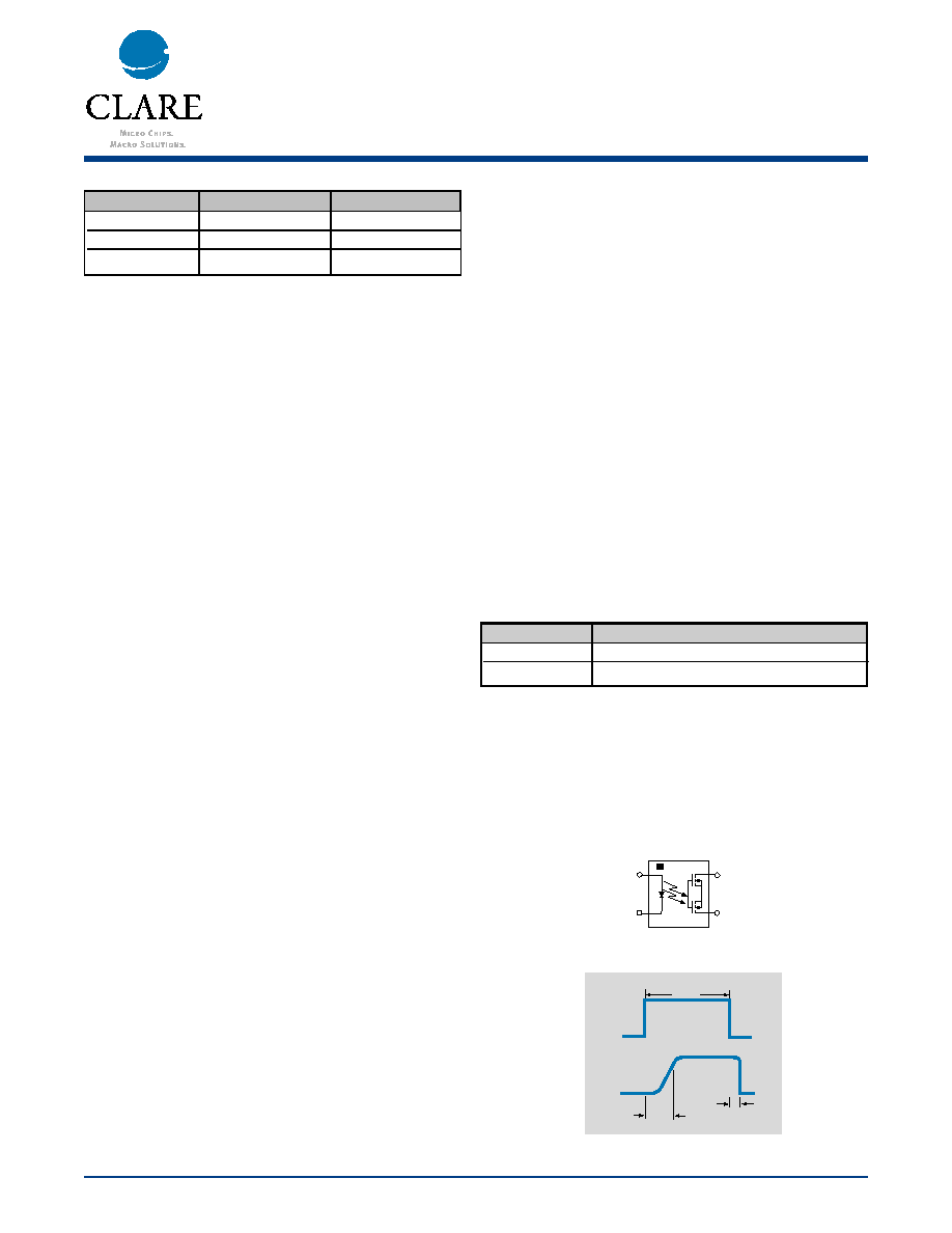
Pin Configuration
CONTROL
LOAD
10ms
10%
10%
90%
+
T
ON
T
OFF
+
+
1
2
3
4
+ Control
– Control
Load
Load
CPC1008N Pinout

www.clare.com
CPC1008N
Rev. 1
Electrical Characteristics
Absolute Maximum Ratings are stress ratings. Stresses
in excess of these ratings can cause permanent damage
to the device. Functional operation of the device at these
or any other conditions beyond those indicated in the
operational sections of this data sheet is not implied.
Exposure of the device to the absolute maximum ratings
for an extended period may degrade the device and effect
its reliability.
Absolute Maximum Ratings (@ 25∞ C)
PARAMETER
CONDITIONS
SYMBOL
MIN
TYP
MAX
UNITS
Output Characteristics @ 25∞C
Load Voltage (Peak)
-
V
L
-
-
100
V
Load Current (Continuous)
1
I
L
-
-
150
mA
Peak Load Current
10ms
I
LPK
-
-
350
mA
On-Resistance
2
I
L
=150mA
R
ON
-
-
8
Off-State Leakage Current
V
L
=100V
I
LEAK
-
-
1
µA
Switching Speeds
Turn-On
I
F
=5mA, V
L
=10V
T
ON
-
-
2
ms
Turn-Off
I
F
=5mA, V
L
=10V
T
OFF
-
0.5
ms
Output Capacitance
50V; f=1MHz
C
OUT
-
25
-
pF
Input Characteristics @ 25∞C
Input Control Current
I
L
=150mA
I
F
2
-
50
mA
Input Dropout Current
-
I
F
0.3
0.9
-
mA
Input Voltage Drop
I
F
=5mA
V
F
0.9
1.2
1.4
V
Reverse Input Voltage
-
V
R
-
-
5
V
Reverse Input Current
V
R
=5V
I
R
-
-
10
µA
1
Load current derates linearly from 150mA @ 25
o
C to 125mA @ 85
o
C.
2
Measurement taken within 1 second of on time.
Parameter
Min
Typ
Max Units
Input Power Dissipation
-
-
70
mW
Input Control Current
-
-
50
mA
Peak (10ms)
-
-
1
A
Reverse Input Voltage
-
-
5
V
Total Power Dissipation
-
-
400
1
mW
Capacitance
Input to Output
-
1
-
pF
Isolation Voltage
Input to Output
1500
-
-
V
RMS
Operational Temperature
-40
-
+85
∞C
Storage Temperature
-40
-
+125
∞C
Soldering Temperature
+220
∞C
(10 Seconds Max.)
1 Derate Linearly 3.33 mw /
o
C
2

CPC1008N
www.clare.com
Rev. 1
PERFORMANCE DATA*
CPC1008N
Typical LED Forward Voltage Drop
(Ambient Temperature = 25 C)
I
F
= 5mADC
35
30
25
20
15
10
5
0
1.17
1.19
1.21
1.23
1.25
LED Forward Voltage Drop (V)
Device Count (N)
o
CPC1008N
Typical On-Resistance Distribution
(Ambient Temperature = 25 C)
(Load Current = 150mA)
35
30
25
20
15
10
5
0
4.40
4.80
5.20
5.60
4.60
5.0
5.40
On-Resistance (
)
Device Count (N)
o
CPC1008N
Typical Blocking Voltage Distribution
(Ambient Temperature = 25 C)
35
30
25
20
15
10
5
0
106
112
118
124
109
115
121
Blocking Voltage (V)
Device Count (N)
o
CPC1008N
Typical I
F
for Switch Operation
(Ambient Temperature = 25 C)
(Load Current = 100mA)
0.75
0.85
0.95
0.70
0.80
0.90
1.0
LED Current (mA)
Device Count (N)
25
20
15
10
5
0
o
CPC1008N
Typical I
F
for Switch Dropout
(Ambient Temperature = 25 C)
(Load Current = 100mA)
25
20
15
10
5
0
0.80
0.90
1.00
0.75
0.85
0.95
1.05
LED Current (mA)
Device Count (N)
o
CPC1008N
Typical Turn-On Time
(Ambient Temperature = 25 C)
(Load Current = 150mA; I
F
= 5mA)
0.25
0.35
0.45
0.55
0.30
0.40
0.50
Turn-On (ms)
Device Count (N)
25
20
15
10
5
0
o
CPC1008N
Typical Turn-Off Time
(Ambient Temperature = 25 C)
(Load Current = 150mA; I
F
= 5mA)
0.21
0.23
0.25
0.27
0.26
0.24
0.22
Turn-Off (ms)
Device Count (N)
25
20
15
10
5
0
o
CPC1008N
Typical MaximumLoad
Current vs. Temperature
Temperature ( C)
Load Current (mA)
190
180
170
160
150
140
130
120
110
100
-40 -20
0
20
40
60
80
120
100
I =5mA
F
I =10mA
F
o
CPC1008N
Typical Leakage vs. Temperature
(Measured across Pins 3 & 4) I
L
= max rated
Temperature ( C)
Leakage (
µ
A)
-40
0.016
0.014
0.012
0.010
0.008
0.006
0.004
0.002
0
-20
0
20
40
60
80
100
o
CPC1008N
Typical Blocking Voltage
vs. Temperature
Temperature ( C)
Blocking Voltage (V
RMS
)
-40
122
121
120
119
118
117
116
115
-20
0
20
40
60
80
100
o
CPC1008N
Typical Turn-On vs. Temperature
(Load Current = 100mA)
Temperature ( C)
5mA
10mA
Turn-On (ms)
-40
5.000
4.500
4.000
3.500
3.000
2.500
2.000
1.500
1.000
0.500
0
-20
0
20
40
60
80
100
o
CPC1008N
Typical Turn-Off vs. Temperature
(Load Current = 100mA)
Temperature ( C)
Turn-Off (ms)
-40
1.000
0.900
0.800
0.700
0.600
0.500
0.400
0.300
0.200
0.100
0
-20
0
20
40
60
80
100
5mA
o
10mA
The Performance data shown in the graphs above is typical of device performance. For guaranteed parameters not indicated in the written specifications, please contact
our application department.
3

www.clare.com
4
CPC1008N
Rev. 1
CPC1008N
Typical LED Forward Voltage Drop
vs. Temperature
Temperature ( C)
LED Forward Voltage Drop (V)
1.8
1.6
1.4
1.2
1.0
0.8
-40 -20
0
20
40
60
80
120
100
50mA
30mA
20mA
10mA
5mA
o
CPC1008N
Typical Turn-On vs. LED Forward Current
(Load Current = 120mA)
LED Forward Current (mA)
Turn-On (ms)
0
5
10 15 20 25 30 35 40 45
2.0
1.8
1.6
1.4
1.2
1.0
0.8
0.6
0.4
0.2
0
50
CPC1008N
Typical Turn-Off vs. LED Forward Current
(Load Current = 120mA)
LED Forward Current (mA)
Turn-Off (ms)
0
5
10 15 20 25 30 35 40 45
0.7
0.6
0.5
0.4
0.3
0.2
0.1
0
50
CPC1008N
Typical On-Resistance vs. Temperature
(Load Current = max rated @ temperature)
Temperature ( C)
On-Resistance ( )
-40
12
10
8
6
4
2
0
-20
0
20
40
60
80
100
o
Steady State
Instantaneous
IF = 5mA
IF = 10mA
IF = 5mA
CPC1008N
Typical I
F
for Switch Operation
vs. Temperature
(Load Current = 100mA)
Temperature ( C)
LED Current (mA)
-40
3.000
2.500
2.000
1.500
1.000
0.500
0
-20
0
20
40
60
80
100
o
CPC1008N
Typical I
F
for Switch Dropout
vs. Temperature
(Load Current = 100mA)
Temperature ( C)
LED Current (mA)
-40
3.000
2.500
2.000
1.500
1.000
0.500
0
-20
0
20
40
60
80
100
o
Load Voltage (V)
Load Current (mA)
150
100
50
0
-50
-100
-150
-1.5
-1.0
-0.5
0
0.5
1.0
1.5
CPC1008N
Typical Load Current vs. Load Voltage
(Ambient Temperature = 25 C)
I
F
= 5mA
o
CPC1008N
Energy Rating Curve
Time
Load Current (A)
10µs
1.0
0.9
0.8
0.7
0.6
0.5
0.4
0.3
0.2
0.1
0
1ms
100µs
100ms 1s
10ms
10s 100s
PERFORMANCE DATA*
*The Performance data shown in the graphs above is typical of device performance. For guaranteed parameters not indicated in the written specifications, please contact
our application department.

CPC1008N
www.clare.com
5
Rev. 1
Dimensions
m m
(inches)
Mechanical Dimensions
PC Board Pattern
(Top View)
2.54
±
0.127
(0.100
±
0.005)
5.66
±
0.14
(0.223
±
0.005)
1.448
(0.057)
0.889
(0.035)
.20 ± .025
(.008 ± .001)
2.54 TYP.
(.100 TYP.)
2.18 MAX.
(.086)
1.01 ± .025
(.040 ± .001)
3.81 ± .13
(.150 ± .005)
6.09 ± .25
(.240 ± .010)
.38 x 45
(.015 x 45 )
.38 TYP.
(.015 TYP.)
4.09 ± 0.20
(0.161 ± 0.008)
4 Pin SOIC Narrow ("N" Suffix)
0.432 ± 0.127
(.017 ± .005)

CLARE LOCATIONS
Clare Headquarters
78 Cherry Hill Drive
Beverly, MA 01915
Tel: 1-978-524-6700
Fax: 1-978-524-4900
Toll Free: 1-800-27-CLARE
Clare Micronix Division
145 Columbia
Aliso Viejo, CA 92656-1490
Tel: 1-949-831-4622
Fax: 1-949-831-4628
SALES OFFICES
AMERICAS
Americas Headquarters
Clare
78 Cherry Hill Drive
Beverly, MA 01915
Tel: 1-978-524-6700
Fax: 1-978-524-4900
Toll Free: 1-800-27-CLARE
Eastern Region
Clare
P.O. Box 856
Mahwah, NJ 07430
Tel: 1-201-236-0101
Fax: 1-201-236-8685
Toll Free: 1-800-27-CLARE
Central Region
Clare Canada Ltd.
3425 Harvester Road, Suite 202
Burlington, Ontario L7N 3N1
Tel: 1-905-333-9066
Fax: 1-905-333-1824
Western Region
Clare
1852 West 11th Street, #348
Tracy, CA 95376
Tel: 1-209-832-4367
Fax: 1-209-832-4732
Toll Free: 1-800-27-CLARE
Canada
Clare Canada Ltd.
3425 Harvester Road, Suite 202
Burlington, Ontario L7N 3N1
Tel: 1-905-333-9066
Fax: 1-905-333-1824
EUROPE
European Headquarters
CP Clare nv
Bampslaan 17
B-3500 Hasselt (Belgium)
Tel: 32-11-300868
Fax: 32-11-300890
France
Clare France Sales
Lead Rep
99 route de Versailles
91160 Champlan
France
Tel: 33 1 69 79 93 50
Fax: 33 1 69 79 93 59
Germany
Clare Germany Sales
ActiveComp Electronic GmbH
Mitterstrasse 12
85077 Manching
Germany
Tel: 49 8459 3214 10
Fax: 49 8459 3214 29
Italy
C.L.A.R.E.s.a.s.
Via C. Colombo 10/A
I-20066 Melzo (Milano)
Tel: 39-02-95737160
Fax: 39-02-95738829
Sweden
Clare Sales
Comptronic AB
Box 167
S-16329 SpÂnga
Tel: 46-862-10370
Fax: 46-862-10371
United Kingdom
Clare UK Sales
Marco Polo House
Cook Way
Bindon Road
Taunton
UK-Somerset TA2 6BG
Tel: 44-1-823 352541
Fax: 44-1-823 352797
ASIA PACIFIC
Asian Headquarters
Clare
Room N1016, Chia-Hsin, Bldg II,
10F, No. 96, Sec. 2
Chung Shan North Road
Taipei, Taiwan R.O.C.
Tel: 886-2-2523-6368
Fax: 886-2-2523-6369
http://www.clare.com
Worldwide Sales Offices
Specification: DS-CPC1008N-R1
©Copyright 2000, Clare, Inc.
OptoMOS
Æ
is a registered trademark of Clare, Inc.
All rights reserved. Printed in USA.
1/12/01
Clare cannot assume responsibility for use of any circuitry other
than circuitry entirely embodied in this Clare product. No circuit
patent licenses nor indemnity are expressed or implied. Clare
reserves the right to change the specification and circuitry, with-
out notice at any time. The products described in this document
are not intended for use in medical implantation or other direct life
support applications where malfunction may result in direct phys-
ical harm, injury or death to a person.