 | –≠–ª–µ–∫—Ç—Ä–æ–Ω–Ω—ã–π –∫–æ–º–ø–æ–Ω–µ–Ω—Ç: CPC1945G | –°–∫–∞—á–∞—Ç—å:  PDF PDF  ZIP ZIP |

1
www.clare.com
CPC1945G
DS-CPC1945G-R1
The CPC1945G is a AC Solid State Switch using patent-
ed waveguide coupling with dual power SCR outputs to
produce an alternative to optocoupler and Triac circuits.
The CPC1945G switches are robust enough to provide a
blocking voltage of up to 400V. In addition, tightly con-
trolled zero cross circuitry ensures switching of AC loads
without the generation of transients. The input and output
circuits are optically coupled to provide 3750V of isolation
and noise immunity between control and load circuits.
As a result the CPC1945G is well suited for industrial
environments where electromagnetic interference would
disrupt the operation of electromechanical relays.
∑
Programmable Control
∑
Process Control
∑
Power Control Panels
∑
Remote Switching
∑
Gas Pump Electronics
∑
Contractors
∑
Large Relays
∑
Solenoids
∑
Motors
∑
Heaters
∑
UL recognized file #: Pending
∑
Load Current up to 1A
∑
Blocking Voltage to 400V
∑
5mA Sensitivity
∑
Zero-Crossing Detection
∑
DC Control, AC Output
∑
Optically Isolated
∑
TTL and CMOS Compatible
∑
Low EMI and RFI Generation
∑
High Noise Immunity
∑
VDE compatible
∑
Machine Insertable, Wave Solderable
Applications
Features
Description
Approvals
AC Solid State Relay
Ordering Information
Part #
Description
CPC1945G
16 Pin DIP (25/Tube)
CPC1945G
Units
AC Operating
120
V
RMS
Voltage
Load Current
1.0 A
On-State 1.6
V
RMS
Voltage Drop
(at IL=1.0A)
Pin Configuration
CPC1965G
16
1
10
+ LED
AC Load
≠ LED
AC Load
8
ZC
www.clare.com
CPC1945G
Rev. 1
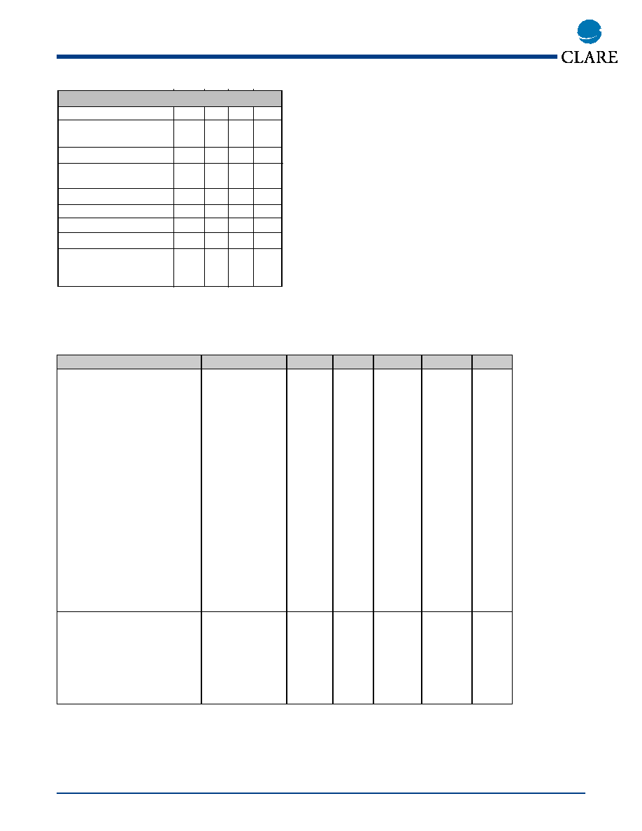
Electrical Characteristics
Absolute Maximum Ratings are stress ratings. Stresses
in excess of these ratings can cause permanent damage
to the device. Functional operation of the device at these
or any other conditions beyond those indicated in the
operational sections of this data sheet is not implied.
Exposure of the device to the absolute maximum ratings
for an extended period may degrade the device and effect
its reliability.
Absolute Maximum Ratings (@ 25∞ C)
2
Parameter
Min
Typ
Max Units
Input Power Dissipation
-
-
150
1
mW
Input Control Current
-
-
50
mA
Peak (10ms)
-
-
1
A
Reverse Input Voltage
-
-
5
V
Total Package Dissipation
PD
-
-
1600
2
mW
Isolation Voltage
Input to Output
3750
-
-
V
RMS
Operational Temperature
-40
-
+85
∞C
Storage Temperature
-40
-
+125
∞C
Soldering Temperature
(10 Seconds Max.)
DIP Package
-
-
+260
∞C
1
Derate Linearly 1.33 mW/∞C
2
Derate Linearly 16.6 mW/∞C
Parameter
Conditions
Symbol
Min
Typ
Max
Units
Output Characteristics @ 25∞C
Operating Voltage Range
V
T
20
-
120
V
RMS
Peak Blocking Voltage
-
V
DRM
-
400
V
Load Current (Continuous)
V
L
=120VAC
I
L
0.005
-
1.0
IA
RMS
Non-repetitive Single Cycle
Surge Current
-
I
TSM
-
-
10
A
Off State Leakage Current
V
DRM
I
LEAK
-
-
1
mA
On-State Voltage Drop
I
L
=1.0A
-
-
1.6
V
RMS
Critical Rate of Rise
3
dv/dt
500
-
-
V/µS
Switching Speeds
Turn-on
I
F
=5 mA
T
ON
-
-
0.5
Cycles
Turn-off
I
F
=5 mA
T
OFF
-
-
0.5
Cycles
Zero-Cross Turn-On Voltage
1st half cycle
-
2
10
V
Sub. half cycle
-
-
1
V
Operating Frequency
1
- 20
-
400
Hz
Load Power Factor for
Guaranteed Turn-On
2
-
PF
0.25
-
-
-
Capacitance
Input to Output
-
-
-
3
-
pF
Input Characteristics @ 25∞C
Input Control Current
For Normal Environment
-
I
F
5
-
50
mA
For High Noise Environment
-
I
F
10
-
100
mA
Input Voltage Drop
I
F
=5mA
V
F
0.9
1.2
1.4
V
Input Drop-out Voltage
-
0.8
-
-
V
Reverse Input Current
V
R
=5V
I
R
-
-
10
uA
1 Zero cross 1st 1/2 cycle @ <100Hz
2 Snubber circuits may be required at low power factors.
3 Tested in accordance with EIA/NARM Standard RS-443.
CPC1945G
www.clare.com
Rev. 1
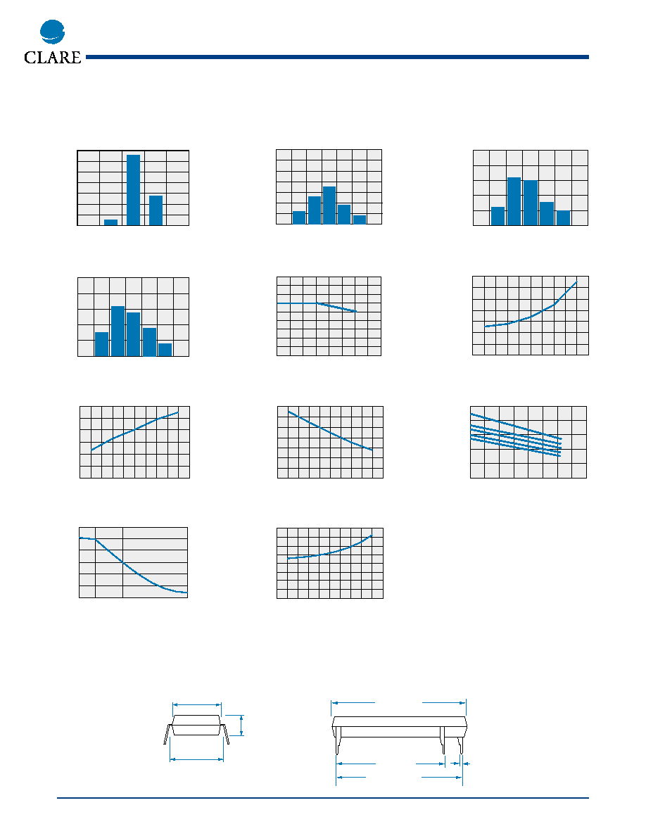
PERFORMANCE DATA*
The Performance data shown in the graphs above is typical of device performance. For guaranteed parameters not indicated in the written specifications, please contact
our application department.
3
16 Pin DIP
7.620 ± .254
(.300 ± .010)
6.350 ± .127
(.250 ± .005)
17.780 TYP.
(.700)
19.202 ± .381
(.756 ± .015)
15.240 TYP.
(.600)
.508 TYP.
(.020)
3.429 TYP.
(.135)
CPC1945G
Typical LED Forward Voltage Drop
(Ambient Temperature = 25 C)
I
F
= 5mADC
35
30
25
20
15
10
5
0
1.17
1.19
1.21
1.23
1.25
LED Forward Voltage Drop (V)
Device Count (N)
o
CPC1945G
Typical On-State Output
Forward Voltage Distribution
(Ambient Temperature = 25 C)
35
30
25
20
15
10
5
0
1.05
1.07
1.09
1.11
1.06
1.08
1.10
Output Forward Voltage
Device Count (N)
o
CPC1945G
Typical I
F
for Switch Operation
(Ambient Temperature = 25∞C)
0.22
0.24
0.26
0.21
0.23
0.25
0.27
LED Current (mA)
Device Count (N)
25
20
15
10
5
0
o
CPC1945G
Typical Blocking Voltage Distribution
(Ambient Temperature = 25∞C)
600
610
620
630
625
615
605
Blocking Voltage
Device Count (N)
25
20
15
10
5
0
o
CPC1945G
Typical Maximum Load
Current vs. Temperature
Temperature ( C)
Load Current (A)
1.6
1.4
1.2
1.0
0.8
0.6
0.4
0.2
0
-40 -20
0
20
40
60
80
120
100
I =5mA
F
o
CPC1945G
Typical Blocking Voltage
vs. Temperature
Temperature (∞C)
Blocking Voltage (V)
#
"
##
%
&#
$#
$"
$!
$
$
$
#'
CPC1945G
Typical Leakage vs. Temperature
@ Maximum Rated Load Voltage
LED Forward Current (mA)
Leakage (mA)
25
40
55
70
85
0.278
0.276
0.274
0.272
0.270
0.268
0.266
0.264
CPC1945G
Typical Output V
F
vs. Temperature
Temperature (∞C)
V-on (V)
25
40
55
70
85
1.100
1.080
1.060
1.040
1.020
1.000
0.980
0.960
CPC1945G
Typical LED Forward Voltage Drop
vs. Temperature
Temperature ( C)
LED Forward Voltage Drop (V)
1.8
1.6
1.4
1.2
1.0
0.8
-40
-20
0
20
40
60
80
120
100
50mA
10mA
5mA
o
30mA
20mA
CPC1945G
Maximum Surge Current (non-repetitive)
(T
J
=50
o
C max)
Pulse Duration (mS)
Peak Surge Current (A)
$
#
&
$
"
CPC1945G
Typical I
F
for Switch Operation
Over Temperature
Temperature (∞C)
Led Current (mA)
25
40
55
70
85
0.400
0.350
0.300
0.250
0.200
0.150
0.100
0.050
0.000
Mechanical Dimensions
Dimensions
mm
(inches)

CLARE LOCATIONS
Clare Headquarters
78 Cherry Hill Drive
Beverly, MA 01915
Tel: 1-978-524-6700
Fax: 1-978-524-4900
Toll Free: 1-800-27-CLARE
Clare Micronix Division
145 Columbia
Aliso Viejo, CA 92656-1490
Tel: 1-949-831-4622
Fax: 1-949-831-4628
SALES OFFICES
AMERICAS
Americas Headquarters
Clare
78 Cherry Hill Drive
Beverly, MA 01915
Tel: 1-978-524-6700
Fax: 1-978-524-4900
Toll Free: 1-800-27-CLARE
Eastern Region
Clare
P.O. Box 856
Mahwah, NJ 07430
Tel: 1-201-236-0101
Fax: 1-201-236-8685
Toll Free: 1-800-27-CLARE
Central Region
Clare Canada Ltd.
3425 Harvester Road, Suite 202
Burlington, Ontario L7N 3N1
Tel: 1-905-333-9066
Fax: 1-905-333-1824
Western Region
Clare
1852 West 11th Street, #348
Tracy, CA 95376
Tel: 1-209-832-4367
Fax: 1-209-832-4732
Toll Free: 1-800-27-CLARE
Canada
Clare Canada Ltd.
3425 Harvester Road, Suite 202
Burlington, Ontario L7N 3N1
Tel: 1-905-333-9066
Fax: 1-905-333-1824
EUROPE
European Headquarters
CP Clare nv
Bampslaan 17
B-3500 Hasselt (Belgium)
Tel: 32-11-300868
Fax: 32-11-300890
France
Clare France Sales
Lead Rep
99 route de Versailles
91160 Champlan
France
Tel: 33 1 69 79 93 50
Fax: 33 1 69 79 93 59
Germany
Clare Germany Sales
ActiveComp Electronic GmbH
Mitterstrasse 12
85077 Manching
Germany
Tel: 49 8459 3214 10
Fax: 49 8459 3214 29
Italy
C.L.A.R.E.s.a.s.
Via C. Colombo 10/A
I-20066 Melzo (Milano)
Tel: 39-02-95737160
Fax: 39-02-95738829
Sweden
Clare Sales
Comptronic AB
Box 167
S-16329 SpÂnga
Tel: 46-862-10370
Fax: 46-862-10371
United Kingdom
Clare UK Sales
Marco Polo House
Cook Way
Bindon Road
Taunton
UK-Somerset TA2 6BG
Tel: 44-1-823 352541
Fax: 44-1-823 352797
ASIA PACIFIC
Asian Headquarters
Clare
Room N1016, Chia-Hsin, Bldg II,
10F, No. 96, Sec. 2
Chung Shan North Road
Taipei, Taiwan R.O.C.
Tel: 886-2-2523-6368
Fax: 886-2-2523-6369
http://www.clare.com
Worldwide Sales Offices
Specification: DS-CPC1945G-R1
©Copyright 2001, Clare, Inc.
All rights reserved. Printed in USA.
1/12/01
Clare cannot assume responsibility for use of any circuitry other
than circuitry entirely embodied in this Clare product. No circuit
patent licenses nor indemnity are expressed or implied. Clare
reserves the right to change the specification and circuitry, with-
out notice at any time. The products described in this document
are not intended for use in medical implantation or other direct life
support applications where malfunction may result in direct phys-
ical harm, injury or death to a person.