 | –≠–ª–µ–∫—Ç—Ä–æ–Ω–Ω—ã–π –∫–æ–º–ø–æ–Ω–µ–Ω—Ç: CPC5710N | –°–∫–∞—á–∞—Ç—å:  PDF PDF  ZIP ZIP |

DS-CPC5710-R1.0
12/16/2002
www.clare.com
1
Features
∑
Excellent common-mode rejection ratio (CMRR),
>40 dB
∑
Supplied application circuits can meet isolation
requirements of worldwide telephony standards
∑
Small 8-pin SOIC
∑
Worldwide telephone network compatibility
∑
Full-wave ringing level detector comparator with
internal threshold, large hysteresis, and logic-level
output
∑
3.3 or 5.0 Volt operation
∑
High differential input impedance, very low common-
mode input impedance
∑
Fixed gain
∑
Differential or single-ended linear output
∑
TTL logic input
∑
CMOS logic output (TTL compatible)
∑
Virtually non-detectable in voice monitoring
applications
Applications
∑
In signal monitoring applications, CPC5710N can be
used for:
∑ Display feature (caller ID) signal processing
∑ Line-in-use detection (another-phone-off-hook)
∑ Ringing signal level detection
∑ Battery presence monitoring
∑ Tip and ring lead voltage monitoring
∑
Line condition detection, including line polarity, tip
and ring lead voltage, and battery presence
Description
The Clare CPC5710N is a CMOS special purpose
fixed-gain amplifier with comparator for telephone line
monitoring. The high (>40 dB) common-mode
rejection ratio makes the CPC5710N an excellent
choice for signal monitoring, discrete voice recording,
and line condition monitoring applications. The
CPC5710N is ideal for modem applications including
embedded modem designs like set-top boxes, and
voice recording applications.
Ordering Information
Figure 1. CPC5710N Block Diagram
Part Number
Description
CPC5710N
Phone line monitor IC, tubed
CPC5710NTR
Phone line monitor IC, tape and reel
IN+
IN-
LIN/CMP
V
DD
V
DD
V
DD
V
SS
V
SS
V
SS
CMPOUT
LINOUT+
LINOUT-
+
+
-
-
-
+
1.625 V
1.25 V
2 V
0 V
A =6
V
3
6
7
1
2
5
4
8
CPC5710N
Phone Line Monitor (PLM) IC

CPC5710N
2
www.clare.com
Rev. 1.0 12/16/2002
1 Specifications . . . . . . . . . . . . . . . . . . . . . . . . . . . . . . . . . . . . . . . . . . . . . . . . . . . . . . . . . . . . . . . . . . . . . . . . . . . . . . . . . . . . . . . . . . . . . . . 3
1.1 Absolute Maximum Ratings . . . . . . . . . . . . . . . . . . . . . . . . . . . . . . . . . . . . . . . . . . . . . . . . . . . . . . . . . . . . . . . . . . . . . . . . . . . . . . . . 3
1.2 Electrical Characteristics . . . . . . . . . . . . . . . . . . . . . . . . . . . . . . . . . . . . . . . . . . . . . . . . . . . . . . . . . . . . . . . . . . . . . . . . . . . . . . . . . . 3
1.3 Environmental Characteristics . . . . . . . . . . . . . . . . . . . . . . . . . . . . . . . . . . . . . . . . . . . . . . . . . . . . . . . . . . . . . . . . . . . . . . . . . . . . . . 4
1.4 Pinout. . . . . . . . . . . . . . . . . . . . . . . . . . . . . . . . . . . . . . . . . . . . . . . . . . . . . . . . . . . . . . . . . . . . . . . . . . . . . . . . . . . . . . . . . . . . . . . . . 4
2 Applications . . . . . . . . . . . . . . . . . . . . . . . . . . . . . . . . . . . . . . . . . . . . . . . . . . . . . . . . . . . . . . . . . . . . . . . . . . . . . . . . . . . . . . . . . . . . . . . . 5
2.1 Another-Phone-Off-Hook (APOH) and Line Polarity Detector . . . . . . . . . . . . . . . . . . . . . . . . . . . . . . . . . . . . . . . . . . . . . . . . . . . . . . 5
2.2 Non-Intrusive Line Monitoring, Display Feature (Caller ID) Signal Reception, and Ring Detection Application . . . . . . . . . . . . . . . . 6
2.2.1 Frequency Response . . . . . . . . . . . . . . . . . . . . . . . . . . . . . . . . . . . . . . . . . . . . . . . . . . . . . . . . . . . . . . . . . . . . . . . . . . . . . . . 6
2.3 Regulatory Issues . . . . . . . . . . . . . . . . . . . . . . . . . . . . . . . . . . . . . . . . . . . . . . . . . . . . . . . . . . . . . . . . . . . . . . . . . . . . . . . . . . . . . . . 6
3 Using CPC5710N. . . . . . . . . . . . . . . . . . . . . . . . . . . . . . . . . . . . . . . . . . . . . . . . . . . . . . . . . . . . . . . . . . . . . . . . . . . . . . . . . . . . . . . . . . . . . 7
3.1 LIN/CMP Input . . . . . . . . . . . . . . . . . . . . . . . . . . . . . . . . . . . . . . . . . . . . . . . . . . . . . . . . . . . . . . . . . . . . . . . . . . . . . . . . . . . . . . . . . . 7
3.2 Amplifier Design Considerations . . . . . . . . . . . . . . . . . . . . . . . . . . . . . . . . . . . . . . . . . . . . . . . . . . . . . . . . . . . . . . . . . . . . . . . . . . . . 7
3.2.1 Linear Amplifier Gain . . . . . . . . . . . . . . . . . . . . . . . . . . . . . . . . . . . . . . . . . . . . . . . . . . . . . . . . . . . . . . . . . . . . . . . . . . . . . . . 7
3.3 Comparator Considerations . . . . . . . . . . . . . . . . . . . . . . . . . . . . . . . . . . . . . . . . . . . . . . . . . . . . . . . . . . . . . . . . . . . . . . . . . . . . . . . . 7
3.3.1 Ringing Signal Detection. . . . . . . . . . . . . . . . . . . . . . . . . . . . . . . . . . . . . . . . . . . . . . . . . . . . . . . . . . . . . . . . . . . . . . . . . . . . . 7
3.3.2 Setting Ring Detection Threshold . . . . . . . . . . . . . . . . . . . . . . . . . . . . . . . . . . . . . . . . . . . . . . . . . . . . . . . . . . . . . . . . . . . . . . 7
4 Power Quality . . . . . . . . . . . . . . . . . . . . . . . . . . . . . . . . . . . . . . . . . . . . . . . . . . . . . . . . . . . . . . . . . . . . . . . . . . . . . . . . . . . . . . . . . . . . . . . 8
5 Manufacturing Information . . . . . . . . . . . . . . . . . . . . . . . . . . . . . . . . . . . . . . . . . . . . . . . . . . . . . . . . . . . . . . . . . . . . . . . . . . . . . . . . . . . . 8
5.1 Package Dimensions . . . . . . . . . . . . . . . . . . . . . . . . . . . . . . . . . . . . . . . . . . . . . . . . . . . . . . . . . . . . . . . . . . . . . . . . . . . . . . . . . . . . . 8
5.2 Soldering . . . . . . . . . . . . . . . . . . . . . . . . . . . . . . . . . . . . . . . . . . . . . . . . . . . . . . . . . . . . . . . . . . . . . . . . . . . . . . . . . . . . . . . . . . . . . . 8
5.2.1 Moisture Reflow Sensitivity . . . . . . . . . . . . . . . . . . . . . . . . . . . . . . . . . . . . . . . . . . . . . . . . . . . . . . . . . . . . . . . . . . . . . . . . . . . 8
5.2.2 Reflow Profile . . . . . . . . . . . . . . . . . . . . . . . . . . . . . . . . . . . . . . . . . . . . . . . . . . . . . . . . . . . . . . . . . . . . . . . . . . . . . . . . . . . . . 9

CPC5710N
Rev. 1.0 12/16/2002
www.clare.com
3
1. Specifications
1.1 Absolute Maximum Ratings
1.2 Electrical Characteristics
V
DD
= 5V, temperature = 25 ∞C unless otherwise indicated.
Parameter
Minimum Maximum
Unit
V
DD
-0.3
6
V
Storage temperature
-40
+125
∞C
Total package power
dissipation
300
mW
Logic input voltage
-0.3
V
DD
+ 0.3
V
Absolute maximum ratings are stress ratings. Stresses in excess of these
ratings can cause permanent damage to the device. Functional operation
of the device at these or any other conditions beyond those indicated in the
operational sections of this data sheet is not implied. Exposure of the
device to the absolute maximum ratings for an extended period may
degrade the device and affect its reliability.
Parameter
Conditions
Minimum
Typical
Maximum
Unit
DC Characteristics
Supply voltage, V
DD
3.0
-
5.5
V
Supply current, I
DD
-
-
10
mA
AC Characteristics
Input Impedance
10
-
-
M
Input offset voltage, V
IO
-
-
40
mV
Input offset current, I
IO
No common-mode signal applied
-
-
35
nA
Input offset current. I
IO
With 12
µA of common-mode signal applied
-
-
125
nA
Output DC bias level
At LINOUT+ or LINOUT-, I
O
@ 0.5 mA
0.9
1.0
1.1
V
Output Low Voltage
Swing
I
O
= 0.5 mA
-
-
50
mV
Gain, A
V
0 to 20 kHz
5.88
6
6.12
-
Common-mode
rejection ratio, CMRR
Using supplied application circuits, with common-mode
current
12
µA, 0 to 120 Hz
40
-
-
dB
Equivalent input noise
voltage, V
N
-
-90
-
dBm/Hz

CPC5710N
4
www.clare.com
Rev. 1.0 12/16/2002
1.3 Environmental Characteristics
1.4 Pinout
Figure 2. Package Pinout
Comparator Threshold Characteristics
Comparator detection
threshold voltage
I
CM
= 0
675
750
850
mV
Comparator detection
threshold voltage
I
CM
= ±12
µA
488
750
1012
mV
Comparator hysteresis
voltage
I
CM
= 0
300
375
450
mV
LIN/CMP Input Characteristics
Input low voltage
V
IL
-
-
0.8
V
Input high voltage
V
IH
2.0
-
-
V
Input high leakage
current (I
IH
)
V
IH
= 2.4 V
-
-
-120
µA
Input low leakage
current (I
IL
)
V
IL
= 0.4 V
-
-
-120
µA
Unless otherwise specified, minimum and maximum values are production testing requirements. Typical values are characteristic of the device and are the result of
engineering evaluations. Typical values are provided for information purposes only and are not part of the testing requirements.
Parameter
Conditions
Minimum
Typical
Maximum
Unit
Parameter
Conditions
Minimum
Typical
Maximum
Unit
Operating temperature
-40
-
+85
∞C
Operating humidity
non-condensing
5
-
95
%
Pin
Name
Description
1
VDD
Power supply
2
CMPOUT
Comparator output, active low
3
LIN/CMP
Output select, low for linear output or high for
comparator output
4
LINOUT-
Negative differential linear output
5
LINOUT+
Positive differential linear output
6
IN+
Positive differential input
7
IN-
Negative differential input
8
VSS
Ground
1
2
3
4
8
7
6
5
VDD
CMPOUT
LIN/CMP
LINOUT-
VSS
IN-
IN+
LINOUT+

CPC5710N
Rev. 1.0 12/16/2002
www.clare.com
5
2. Applications
2.1 Another-Phone-Off-Hook (APOH) and Line Polarity Detector
This circuit performs two additional phone line
interface functions, APOH and line polarity detection.
The APOH output is logic low if another phone
connected in parallel to the detector is off-hook,
specifically, if the tip lead to ring lead voltage is less
than approximately 18 V.
The polarity output indicates the polarity of the phone
line. If tip is positive with respect to ring, polarity out
will be high.
Figure 3. APOH and Polarity Detection Application Circuit
IN+
IN-
LIN/CMP
V
DD
V
DD
V
DD
V
SS
V
SS
V
SS
CMPOUT
LINOUT+
+V
+V
+V
IN-
IN+
IN-
IN+
IN-
IN+
OUT
OUT
OUT
LINOUT-
A
A
A
A
A
+
+
-
-
-
+
1.625 V
1.25 V
A =6
V
U1 CPC5710
1/4 U2
LM339
1/4 U2
LM339
1/4 U2
LM339
APOH
OUT
Polarity
OUT
R1-4
8.06 M
1% EIA
1206
R5
604 K
R17
4.7 M
R10
21 K
R15
10 K
R14
4.7 M
R16
10 K
R6
4.7 M
R7
21 K
R8
20 K
R12
20 K
R13
20 K
R9
499 K
R11
499 K
C1
1 nF
TIP
RING
Unless noted otherwise:
All resistors 1%, 1/16 W.
All capacitors 16 V 10%.
2 V
0 V

CPC5710N
6
www.clare.com
Rev. 1.0 12/16/2002
2.2 Non-Intrusive Line Monitoring, Display Feature (Caller ID) Signal
Reception, and Ring Detection Application
This application uses the logic input LIN/CMP to select
between detecting ringing or passing through display
feature (caller-ID) and voice signals. Note the AC
coupling of the tip and ring signals.
With this circuit, set LIN/CMP high to detect ringing.
After a valid ring, set LIN/CMP low to couple the audio
channel signal to the output pins.
Please see
"Comparator Considerations" on page 7
for
more information on ringing detection.
Figure 4. Non-Intrusive Line Monitoring, Display Feature (Caller ID) Signal Reception, and Ring Detection
Application Circuit
2.2.1 Frequency Response
The blocking capacitors used in this application circuit
affect the frequency response of the system. With the
components shown, response rolls off 3 dB @ 166 Hz.
Other values can be used for different response
characteristics.
2.3 Regulatory Issues
Component sizing and value recommendations shown
in the application circuits above will need to be
reviewed with regard to the regulatory requirements of
any particular application.
IN+
IN-
LIN/CMP
V
DD
V
DD
V
DD
V
SS
V
SS
V
SS
CMPOUT
RING DETECT
(to ring parser)
LINOUT+
Display Feature Output
V
= V at 500 Hz
OUT
IN
3.3 or 5 V
LINOUT-
A
+
+
-
-
-
+
1.625 V
1.25 V
A =6
V
U1 CPC5710
R1-4
1.8 M
(R
)
SNP
C1,2
220 pF
(C
)
SNP
R5
(R
)
1.5 M, 1%
0603
SNPD
TIP
RING
From
Control
Logic
2 V
0 V
Unless noted otherwise:
1/8 W,
All resistors are
1%, 1206.
All capacitors are 2 kV, 10%.
CPC5710N
Rev. 1.0 12/16/2002
www.clare.com
7
3. Using CPC5710N
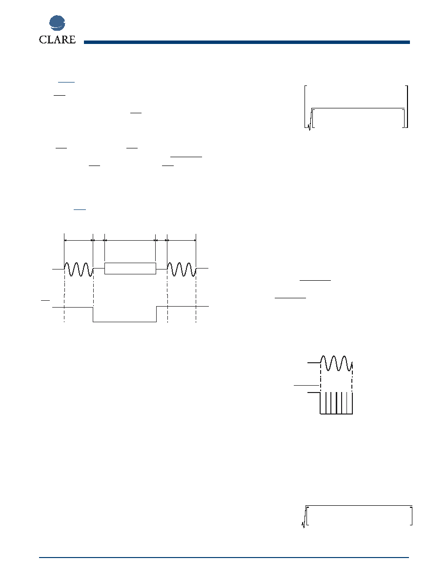
3.1 LIN/CMP Input
The LIN/CMP input selects the active output, either
the comparator output CMPOUT or the linear outputs,
LINOUT- and LINOUT+. Set LIN/CMP low for linear
output and high for comparator output. Note that both
outputs cannot be used at once.
With LIN/CMP at logic low (LIN/CMP = 0), the
amplifier outputs are biased at 1 Vdc and CMPOUT is
held high. With LIN/CMP at logic high (LIN/CMP = 1),
LINOUT+ is 0 V and LINOUT- is 2 V.
Figure 5. LIN/CMP Timing for Caller-ID Signal
Reception
3.2 Amplifier Design
Considerations
Amplifier inputs are biased at 1.25 Vdc, the internal
voltage references. The internal common-mode
circuitry maintains the average of the inputs at 1.25
Vdc. For example, if one input reaches 1.3 V, the
common-mode circuit drives the other input to 1.2 V.
3.2.1 Linear Amplifier Gain
Display feature information (caller ID) and voice
signals are coupled through the linear amplifier. In
North America, CID data signals are typically sent
between the first and second ringing signal burst.
Referring to Figure 4, signal gain from tip and ring to
LINOUT+ and LINOUT- is determined by:
where
is the frequency of the signal.
Clare Application Note AN-117
Customize Caller ID Gain
and Ring Detect Voltage Threshold
is a spreadsheet for
trying different component values in this type of circuit.
3.3 Comparator Considerations
3.3.1 Ringing Signal Detection
The CPC5710N comparator is a full-wave
configuration. Ringing signals will assert the output on
positive and negative parts of the ringing waveform.
Hysteresis is employed in the internal comparator
circuit to provide noise immunity. The set-up of the
comparator causes CMPOUT output pulses to remain
low for most of the ringing signal positive and negative
half-cycles. CMPOUT returns high when the ringing
signal is near the zero-voltage crossing.
Figure 6. CMPOUT Relative to Ring Signal
3.3.2 Setting Ring Detection Threshold
The ring detection threshold depends on the
component values of the input network. The values for
these components shown in the typical application
circuits are recommended for typical operation.
Referring to Figure 4, the ring detection threshold can
be changed according to the following formula:
Caller ID data
LIN/CMP
Signal levels not to scale
2s
500 ms
3s
475 ms
2s
GAIN
CID
dB
(
)
20
6R
SNPD
4R
SNP
R
SNPD
+
(
)
2
1
fC
SNP
(
)
2
--------------------------
+
-----------------------------------------------------------------------------------------
log
=
CMPOUT
Ring Signal
V
RINGPK
750mV
R
RSNPD
-------------------
4R
SNP
R
SNPD
+
(
)
2
1
f
RING
C
SNP
(
)
2
--------------------------------------
+
=

CPC5710N
8
www.clare.com
Rev. 1.0 12/16/2002
With the application circuit in Figure 4, the series
capacitors serve to reduce the magnitude of high-
amplitude, low-frequency ring signals, making the ring
detection threshold of the CPC5710N variable with the
frequency the ringing signal. With the circuit as given,
CMPOUT will change states with a 15 Hz ringing
signal at approximately 48 V
PEAK
. For a 68 Hz ring
signal, CMPOUT will change states with a ringing
signal amplitude of approximately 11.5 V
PEAK
.
In applications where CPC5710N will be used only as
a ring level detector, or if significant attenuation of the
amplified signal can be tolerated, the frequency
variability of the ring detection threshold can be
reduced by increasing the value of the resistors and
capacitors in series with the input.
Clare Application Note AN-117
Customize Caller ID Gain
and Ring Detect Voltage Threshold
is a spreadsheet for
trying different component values in this circuit for
LITELINK snoop circuit applications.
4. Power Quality
CPC5710N works best with a clean power supply. To
clean up power supply noise, Clare, Inc., recommends
using a pi network on the V
DD
pin as shown in
Figure 7, if needed.
Figure 7. Optional Power Supply pi Network
Note: For lower-frequency noise, use a 220
µ
H
inductor in series with R100.
5. Manufacturing Information
The CPC5710N branding (package imprinting) leaves
off the last character of the part number due to
package space limitations.
5.1 Package Dimensions
CPC5710N uses JEDEC standard 8-pin SOIC
packaging. See
JEDEC Publication 95, MS-012
for 3.75
(0.150) small-outline package dimensions.
5.2 Soldering
5.2.1 Moisture Reflow Sensitivity
Clare has characterized the moisture reflow sensitivity
of this product using IPC/JEDEC standard J-STD-
020A and classifies it as MSL (Moisture Sensitivity
Level) 1, not moisture sensitive.
3.3 or 5 V
R100
10
To V
Pin 1
DD
A
A
C101
10
FB100
600
200 mA
C100
1

5.2.2 Reflow Profile
The maximum ramp rates, dwell times, and
temperatures of the assembly reflow profile should not
exceed those specified in IPC/JEDEC standard J-
STD-020A, which were used to determine the
moisture sensitivity level of this component.
For additional information please visit
www.clare.com
Clare, Inc. makes no representations or warranties with respect to the accuracy or completeness of the contents of this publication and reserves the right to make
changes to specifications and product descriptions at any time without notice. Neither circuit patent licenses or indemnity are expressed or implied. Except as set
forth in Clare's Standard Terms and Conditions of Sale, Clare, Inc. assumes no liability whatsoever, and disclaims any express or implied warranty relating to its
products, including, but not limited to, the implied warranty of merchantability, fitness for a particular purpose, or infringement of any intellectual property right.
The products described in this document are not designed, intended, authorized, or warranted for use as components in systems intended for surgical implant into
the body, or in other applications intended to support or sustain life, or where malfunction of Clare's product may result in direct physical harm, injury, or death to a
person or severe property or environmental damage. Clare, Inc. reserves the right to discontinue or make changes to its products at any time without notice.
Specification: DS-CPC5710N-R1.0
© Copyright 2002, Clare, Inc.
All rights reserved. Printed in USA.
12/16/2002