 | –≠–ª–µ–∫—Ç—Ä–æ–Ω–Ω—ã–π –∫–æ–º–ø–æ–Ω–µ–Ω—Ç: CYG2030 | –°–∫–∞—á–∞—Ç—å:  PDF PDF  ZIP ZIP |
1
www.clare.com
CYG20XX
DS-CYG20XX-R1
The CYG2000/2001/2010/2011/2020/2021/2030/2031
are Data Access Arrangement (DAA) modules featuring
a 350V, 120mA, 15
relay used for hookswitch, optocou-
pler with minimum CTR of 33% for ring detection, and a
low distortion transformer with 28.8kbps capabilities.
∑
Modems
∑
Fax machines
∑
Remote data acquisition
∑
Security systems
∑
Voice mail systems
∑
PC motherboard
∑
Computer telephony
∑
Process control
∑
Medical
∑
PBX
∑
Direct broadcast satellite
∑
UL recognized file #: E174201
∑
Low distortion transformer signal coupling
(0.01% max)
∑
Complete ring detector circuit
∑
Low power hookswitch
∑
Electronic inductor/gyrator circuit
∑
Surge protection
∑
Transient protection zeners
∑
Half- (20X0) or Full- (20X1) Wave Detection
∑
V.32 bis /V.34 compatible
∑
FCC Compatible
∑
Compatible with U.S. and Canadian dial up
phone lines
∑
Supports leased-line operation
∑
PC board mountable
Applications
Features
Description
Approvals
Cybergate
TM
Ordering Information
Part #
Description
CYG2000
DAA Module, Half Wave Ring Detection
CYG2001
DAA Module, Full Wave Ring Detection
CYG2010
DAA Module, Half Wave Ring Detection,
Loop Current Detection
CYG2011
DAA Module, Full Wave Ring Detection
Loop Current Detection
CYG2020
DAA Module, Half Wave Ring Detection,
CID
CYG2021
DAA Module, Full Wave Ring Detection,
CID
CYG2030
DAA Module, Half Wave Ring Detection,
CID and Loop Current Detection
CYG2031
DAA Module, Full Wave Ring Detection,
CID and Loop Current Detection
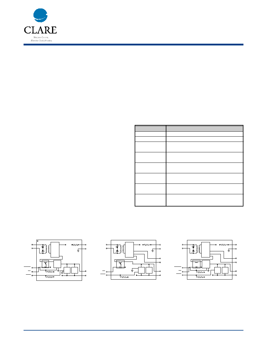
Block Diagrams
8
7
9
RING
OH
LOOPI
1
2
17
18
11
10
HOOKSWITCH
LINE 2
LINE 1
RING
GND
V
CC
GND
470
V
CC
TIP
RING
GYRATOR
V
CC
RING
V
CC
V
CC
2.2k
47k
LOOP
CURRENT
DETECT
RING
DETEC-
TION
SURGE
PROTEC-
TION
CYG2010/CYG2011
R_LIM
R_LIM
8
9
RING
OH
1
2
17
18
11
10
14
13
HOOKSWITCH
LINE 2
LINE 1
RING
GND
V
CC
V
CC
TIP
RING
GYRATOR/
CALLER ID
RING
R_LIM
R_LIM
V
CC
47k
RING
DETEC-
TION
SURGE
PROTEC-
TION
CID1
CID2
CYG2020/CYG2021
470
8
7
9
RING
OH
LOOPI
1
2
17
18
11
10
14
13
HOOKSWITCH
LINE 2
LINE 1
RING
GND
V
CC
V
CC
TIP
RING
GYRATOR/
CALLER ID
V
CC
RING
R_LIM
R_LIM
V
CC
2.2k
47k
LOOP
CURRENT
DETECT
RING
DETEC-
TION
SURGE
PROTEC-
TION
CID1
CID2
CYG2030/CYG2031
470
Handling and Assembly Recommendations
The CYG20XX products are not hermetically sealed and should not be exposed to any liquid-based rinsing processes. Clare recommends two (2) approaches. The
modem should either use a no clean soldering flux that would mostly evaporate during the normal wave soldering processes, or be soldered in by hand after the
rest of the card is wave soldered.
www.clare.com
CYG20XX
Rev. 1
Electrical Characteristics
Absolute Maximum Ratings are stress ratings. Stresses in
excess of these ratings can cause permanent damage to
the device. Functional operation of the device at these or
any other conditions beyond those indicated in the opera-
tional sections of this data sheet is not implied. Exposure
of the device to the absolute maximum ratings for an
extended period may degrade the device and effect its
reliability.
Absolute Maximum Ratings (@ 25∞ C)
2
Parameter
Conditions
Min
Typ
Max
Unit
DC Electrical Characteristics
On-Hook Impedance
@100VDC across pins
10
-
-
M
10,11 (R,T), per FCC 68.312
Off-Hook Line Leakage Current
@100VDC across pins
-
-
10
µA
10,11 (R,T), per FCC 68.312
Hookswitch Resistance
-
-
-
15
Off-Hook Supply Current
@+5V, V
CC
7
8
9
mA
Hookswitch Power Source, Pin 8
-
4.75
5.0
20
V
DC Loop Current
-
20
-
120
mA
AC Signal Path Electrical Characteristics
Return Loss
300-3500Hz
18
25
-
dB
Insertion Loss
300-3500Hz
Transmit
Test Circuit 1
-
-
7
dB
Receive
Test Circuit 2
-
-
7
dB
Frequency Response
300-3500Hz
-0.25
-
+0.25
dB
Longitudinal Balance
On-Hook
Per FCC 68.310
60
-
-
dB
Off-Hook
Per FCC 68.310
40
-
-
dB
DC Loop Current
-
20
-
120
mA
Total Harmonic Distortion
@600Hz and -10dBm
-
-
0.01
%
Secondary Load Impedance
Line 1 and Line 2
-
294
-
Primary Source Impedance
Tip and Ring
-
600
-
Ring Detection Circuit Characteristics
Ringing Voltage Detection Range
-
20
-
150
Vrms
Ringing Frequency Detection Range
-
15
-
70
Hz
Ringer Equivalence Number
-
-
0.8B
-
RING (Pin 9) Output Voltage (Pulsed)
V
CC
@+5V
Logic `0', Ring present
-
-
0.8
V
Logic `1', Ring not present
-
-
Vcc
V
Parameter
Min
Typ
Max Units
Isolation Voltage
-
-
1000 V
RMS
Operational Temperature
0
-
70
∞C
Storage Temperature
0
-
70
∞C
Relative Humidity
(Non-Condensing)
10
-
85
%
Soldering Temperature
-
-
260
∞C
Tip/Ring (5, 6) Load
current (continuous)
-
-
120
mA
Hookswitch LED
Drive Current
-
-
50
mA
Hookswitch LED
Reverse Voltage
-
-
5
V
Ring Detect
Phototransistor Voltage V
CC
-
-
20
V
CYG20XX
www.clare.com
Rev. 1
3
Electrical Characteristics (Continued)
Parameter
Conditions
Min
Typ
Max
Unit
Surge, Transient, and
Isolation Characteristics
Surge Protection Voltage Tip and Ring
-
-
-
300
V
(Pins 11,10)
Transient Voltage Protection on
Line 1 and Line 2 (Pins 1,2)
-
-5
-
+5
V
Isolation Voltage
(Pins 1,2,7,8,9,17,18 to10,11,13,14)
Per FCC 68.302
-
-
1000
V
RMS
Loop Detection Characteristics
(CYG2010/CYG2011/CYG2030/CYG2031)
Loop Current Detection Threshold
Internal optocoupler with
9
10
11
mA
2.2K Pull-up resistor
Test Circuits
LINE1
LINE2
+V
BATT
-V
BATT
OH
RING
10H
600
10H
TIP
RING
V
CC
GND
CID1
CID2
V
R
+5V
V
LR
I
LOOP
G
Log
V
V
RC
R
LR
=
20
Receive Insertion Loss =
2. CYG20XX Receive Insertion Loss
AC
Source
Rm
294
LINE1
LINE2
+5V
+V
BATT
-V
BATT
OH
RING
10H
600
10H
TIP
RING
V
CC
GND
CID1
CID2
LOOP
Rm
294
V
T
V
LT
I
LOOP
G
Log
V
V
TR
LT
T
=
20
Transmit Insertion Loss =
1. CYG20XX Transmit Insertion Loss
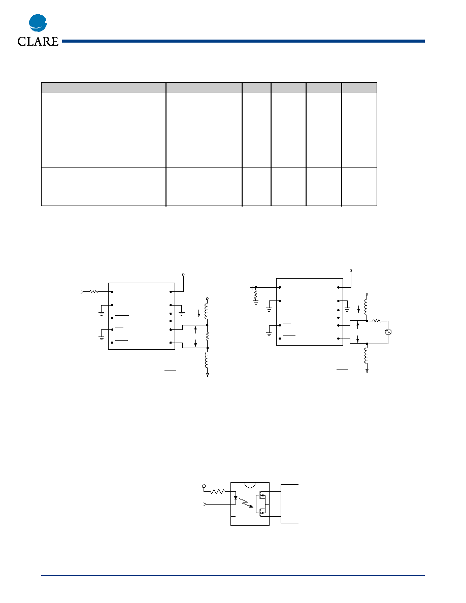
1
2
4
6
V
CC
µ
P Control
(Active Low)
CID1
CID2
CYG2020/2021/2030/2031
Caller ID Connections
Pins 13 & 14 should be connected to a 1-Form-A solid state relay (Clare LCA110), as follows:

www.clare.com
4
CYG20XX
Rev. 1
Package Pinouts
Top View
18
17
1
2
8
7
9
11
10
V
CC
GND
TIP
RING
LINE 1
LINE 2
DO NOT USE
OH
RING
CYG2000/CYG2001
Top View
18
17
1
2
8
9
11
10
V
CC
GND
TIP
RING
14
13
CID1
CID2
LINE 1
LINE 2
OH
RING
CYG2020/CYG2021
Top View
18
17
1
2
8
7
9
11
10
V
CC
GND
TIP
RING
LINE 1
LINE 2
LOOPI
OH
RING
CYG2010/CYG2011
Top View
18
17
1
2
8
7
9
11
10
V
CC
GND
TIP
RING
14
13
CID1
CID2
LINE 1
LINE 2
LOOPI
OH
RING
CYG2030/CYG2031
CYG20XX Pinouts & Definitions
PIN#
I/O
Name
Function
1
I/O
LINE1
Transformer isolated audio signal coupling path for the telephone line.
2
I/O
LINE2
Transformer isolated audio signal coupling path for the telephone line.
7
I
LOOPI
When system is off-hook (OH driven LOW) LOOPI is driven LOW continuously
on CYG2010/2011/2030/2031 devices.
N/C
Keying pin for CYG2000/CYG2001, do not use.
8
I
OH
Driving this pin LOW asserts the off-hook condition. The hookswitch LED is cur-
rent limited by an internal 470
resistor.
9
O
RING
Active LOW indicates an incoming ring signal. This is pulsed LOW by the AC
ring signal at the ring frequency from 15-40Hz.
10
I/O
RING
Connection to telephone line Ring conductor.
11
I/O
TIP
Connection to telephone line Tip conductor.
13
O
CID2
Caller ID connection on CYG2020/2021/2030/2031. CID1/CID2 connect to an
external 1-Form-A solid state relay (CP Clare LCA110). When the SSR is closed
(connecting CID1 to CID2) Caller ID information is presented to LINE1/LINE2
after the first telephone ring burst.
14
O
CID1
Caller ID connection. See CID2 above.
17
I
GND
Connected to host system ground.
18
I
V
CC
Provides power to the hookswitch LED. Typically +5V for
8mA LED current.
LED is current limited by an internal 470
resistor. V
CC
should not exceed 20V.

CYG20XX
www.clare.com
5
Rev. 1
HYBRID
CIRCUIT
8
9
RING
OH
294
1
2
10
+5V
18
11
17
TO TELEPHONE LINE
GYRATOR
SURGE
PROTECTOR
RING
DETECT
NETWORK
V
CC
V
CC
470
56k
HOOKSWITCH
V
CC
LINE 2
LINE 1
RING
GND
GND
V
CC
TX1
TX2
RX
OH RELAY
RING
TIP
CYG2000/CYG2001
Typical Application