ITC117PL
Units
Relay Blocking Voltage
350
V
Relay Load Current
120
mA
Relay Max R
ON
20
Bridge Rectifier Reverse
Voltage
100
V
Darlington Collector Current
120
mA
Darlington Current Gain
10,000
-
Part #
Description
ITC117PL
16 Pin SOIC (50/Tube)
ITC117PLTR
16 Pin SOIC (1000/Reel)
www.clare.com
DS-ITC117PL-R1.0
ITC117PL
Integrated Telecom Circuits
1
Applications
Features
Description
Approvals
Ordering Information
Pin Configuration
The Integrated Telecom Circuit combines a 1-Form-A
solid state relay, bridge rectifier, Darlington transistor
and optocoupler into one 16 pin SOIC package, con-
solidating designs and reducing component count in
telecom applications. The relay features the added
benefit of current limiting. The ITC117's optocoupler
provides for full wave detection of ring signals.
�
Data/Fax Modem
�
Voice Mail Systems
�
Telephone Sets
�
Computer Telephony Integration
�
Set Top Box Modems
�
UL Recognized: File Number E76270
�
CSA Certified: File Number LR 43639-12
�
Certified to:
�
EN 60950
�
EN 41003
�
IEC 950
�
AS/NZS 3260
�
Small 16 Pin SOIC Package (PCMCIA Compatible)
�
Board Space and Cost Savings
�
2mW Hookswitch Drive Power (Logic Compatible)
�
No Moving Parts
�
3750V
RMS
Input/Output Isolation
�
Full-Wave Bridge Rectifier
�
Darlington Transistor for Electronic Inductor "Dry"
Circuits
�
Full Wave Current Detector for Ring Signal or Loop
Current Detect
�
Current Limiting
�
JEDEC Standard Lead Configuration
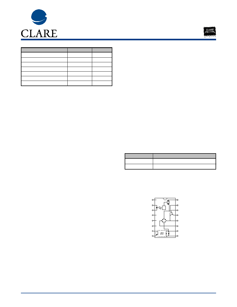
ITC117PL
PV
1
2
3
4
16
15
14
13
5
6
7
8
(N/C)
� LED - Form A Relay
� LED - Form A Relay
(N/C)
(N/C)
(N/C)
Collector - Phototransistor
Emitter - Phototransistor
Output Form A
Output Form A/Bridge Input �/+
Darlington Base
Darlington Emitter
Bridge Output +/Darlington Collector
Bridge Output �
LED - Phototransistor �/+
LED - Phototransistor +/�
12
11
10
9
**
**
Denotes full-wave detection
Parameter
Conditions
Symbol
Min
Typ
Max
Units
Relay Portion (Pins 15,16)
Output Characteristics @ 25�C
Load Current (Continuous)
-
I
L
-
-
120
mA
On-Resistance
I
L
=120mA
R
ON
-
-
20
Off-State Leakage Current
V
L
=350, T
J
=25�C
I
LEAK
-
-
1
�A
Switching Speeds
Turn-On
I
F
=5mA, V
L
=10V
T
ON
-
-
5
ms
Turn-Off
I
F
=5mA, V
L
=10V
T
OFF
-
-
3
ms
Output Capacitance
50V, f=1MHz
C
OUT
-
25
-
pF
Current Limit
I
F
=5mA
I
CL
190
235
280
mA
Relay Portion (Pins 2,3)
Input Characteristics @ 25�C
Input Control Current
I
L
=120mA
I
F
5
-
50
mA
Input Voltage Drop
I
F
=5mA
V
F
0.9
1.2
1.4
V
Reverse Input Voltage
-
V
R
-
-
5
V
Reverse Input Current
V
R
=5V
I
R
-
-
10
�A
Detector Portion (Pins 7,8)
Output Characteristics @ 25�C
Phototransistor Blocking
Voltage
I
C
=10�A
BV
CEO
20
50
-
V
Phototransistor Dark Current
V
CE
=5V, I
F
=0mA
I
CEO
-
50
500
A
Saturation Voltage
I
C
=2mA, I
F
=16mA
V
SAT
-
0.3
0.5
V
Current Transfer Ratio
IF=6mA, V
CE
=0.5V
CTR
33
400
-
%
Detector Portion (Pins 9,10)
Input Characteristics @ 25�C
Input Control Current
I
C
=2mA, V
CE
=0.5V
I
F
6
2
100
mA
Input Voltage Drop
I
F
=5mA
V
F
0.9
1.2
1.4
V
Input Current
I
C
=1�A, V
CE
=5V
I
F
5
25
-
�A
(Detector must be off)
Parameter
Min
Typ Max Units
Total Package Dissipation
-
-
1
1
W
Isolation Voltage
Input to Output
3750
-
-
V
RMS
Relay Blocking Voltage
-
-
350
V
Operational Temperature
-40
-
+85
�C
Storage Temperature
-40
-
+125
�C
Soldering Temperature
-
-
+220
�C
(10 Seconds Max.)
1
Above 25� derate linerity 8.33mw/�C
Total Power Dissipation (PD):
P
D
=P
HOOKSWITCH
+ P
BRIDGE
+ P
DARLINGTON
+ P
LED
P
D
=(R
DS
(on)) (I
2
L
) + 2(V
F
)(I
L
) + (V
CE
)(I
L
) + (V
LED
)(I
F
)
WHERE:
R
DS
(on) = Maximum realy on resistance
I
L
= Maximum loop current
V
F
= Maximum diode forward voltage
V
CE
= Maximum voltage collector to emitter
V
LED
= Maximum LED forward voltage
I
F
= Maximum LED current
www.clare.com
2
ITC117PL
Rev. 1.0
Absolute Maximum Ratings are stress ratings. Stresses in
excess of these ratings can cause permanent damage to
the device. Functional operation of the device at these or
any other conditions beyond those indicated in the opera-
tional sections of this data sheet is not implied. Exposure
of the device to the absolute maximum ratings for an
extended period may degrade the device and effect its
reliability.
Absolute Maximum Ratings (@ 25� C)
Electrical Characteristics
Parameter
Conditions
Symbol
Min
Typ
Max
Units
Bridge Rectifier Electrical
Ratings @ 25�C
Reverse Voltage
-
V
RD
-
-
100
V
Forward Drop Voltage
I
FD
=120mA
V
FD
-
-
1.5
V
Reverse Leakage Current
T
J
=25�C, V
R
=100V
I
RD
-
-
10
�A
T
J
=85�C
-
-
50
-
Forward Current (Continuous)
I
FD
-
-
140
mA
Forward Current (Peak)
t=10mS
I
FD
-
-
0.5
A
Darlington Electrical
Ratings @ 25�C
Collector-Emitter Voltage
I
c
=10mA DC, I
B
=0
V
CEO
40
-
-
V
Collector-Current Continuous
V
C
=3.5V
I
C
-
-
120
mA
Power Dissipation @ 25�C
-
P
d
-
-
500
mW
Off-State Collector Emitter
Leakage Current
V
CE
=10V; I
B
=0mA
I
CEX
-
-
1
�A
DC Current Gain
I
C
=120mA,
h
FE
10,000
-
-
V
CE
=10VDC
Saturation Voltage
I
C
=120mA
V
CE(SAT)
-
-
1.5
V
Total Harmonic Distortion
fo=300Hz @ -10dBm
-
-
-
-80
dB
I
C
=40mA
ITC117PL
www.clare.com
3
Rev. 1.0
Electrical Characteristics
www.clare.com
4
ITC117PL
Rev. 1.0
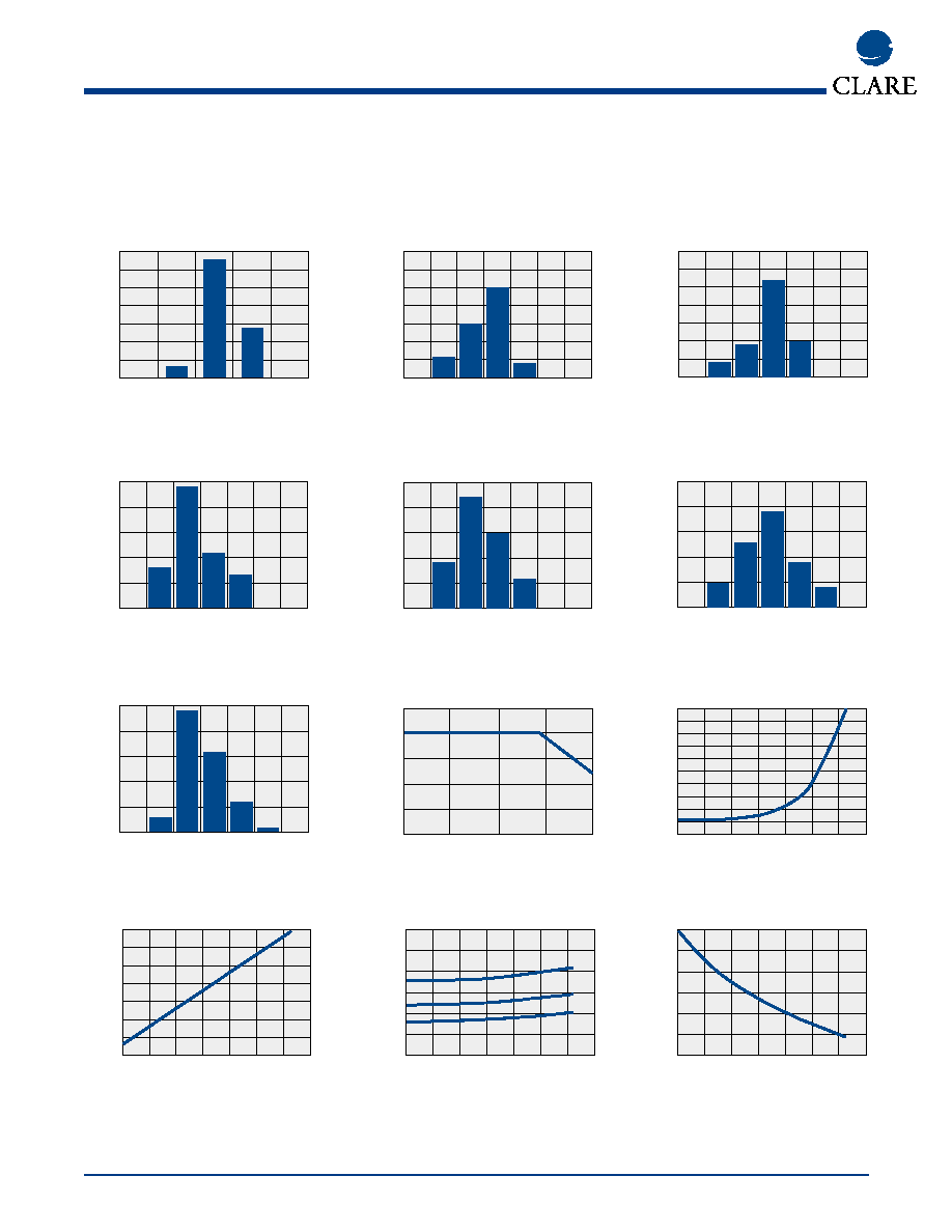
PERFORMANCE DATA*
* The Performance data shown in the graphs above is typical of device performance. For guaranteed parameters not indicated in the written specifications, please contact our application
department.
ITC117PL
Typical LED Forward Voltage Drop
(N=50 Ambient Temperature = 25
�C)
I
F
= 5mADC
35
30
25
20
15
10
5
0
1.17
1.19
1.21
1.23
1.25
LED Forward Voltage Drop (V)
Device Count (N)
ITC117PL
Typical On-Resistance Distribution
(N=50 Ambient Temperature = 25
�C)
(Load Current = 120mADC; I
F
=2mADC)
35
30
25
20
15
10
5
0
17.0
17.8
18.6
19.4
17.4
18.2
19.0
On-Resistance (
)
Device Count (N)
ITC117PL
Typical Blocking Voltage Distribution
(N=50 Ambient Temperature = 25
�C)
35
30
25
20
15
10
5
0
365
385
405
425
375
395
415
Blocking Voltage (V)
Device Count (N)
ITC117PL
Typical I
F
for Switch Operation
(N=50 Ambient Temperature = 25
�C)
(Load Current = 120mADC)
0.42
0.66
0.90
0.30
0.54
0.78
1.02
LED Current (mA)
Device Count (N)
25
20
15
10
5
0
ITC117PL
Typical I
F
for Switch Dropout
(N=50 Ambient Temperature = 25
�C)
(Load Current = 120mADC
25
20
15
10
5
0
0.30
0.54
0.78
0.18
0.42
0.66
0.90
LED Current (mA)
Device Count (N)
)
ITC117PL
Typical Turn-On Time
(N=50 Ambient Temperature = 25
�C)
(Load Current = 120mADC; I
F
= 2mADC)
0.88
1.58
2.28
2.98
1.23
1.93
2.63
Turn-On (ms)
Device Count (N)
25
20
15
10
5
0
ITC117PL
Typical Turn-Off Time
(N=50 Ambient Temperature = 25
�C)
(Load Current = 120mADC; I
F
= 2mADC)
0.06
0.14
0.22
0.30
0.26
0.18
0.10
Turn-Off (ms)
Device Count (N)
25
20
15
10
5
0
ITC117PL
Load Current vs. Ambient Temperature
Ambient Temperature (
�C)
Percent of Maximum
Load Rating (Typical) (%)
-40
100
75
50
25
0
0
25
50
85
I
F
= 5mA
ITC117PL
Typical Leakage vs. Temperature
(Measured across Pins 15 & 16)
Temperature (
�C)
Leakage (
�
A)
-40
0.10
0.09
0.08
0.07
0.06
0.05
0.04
0.03
0.02
0.01
0
-20
0
20
40
60
80
100
ITC117PL
Typical Blocking Voltage
vs. Temperature
Temperature (
�C)
Blocking Voltage (V
RMS
)
-40
415
410
405
400
395
390
385
380
-20
0
20
40
60
80
100
ITC117PL
Typical Turn-On vs. Temperature
(Load Current = 120mADC)
Temperature (
�C)
Turn-On (ms)
-40
3.0
2.5
2.0
1.5
1.0
0.5
0
-20
0
20
40
60
80
100
5mA
10mA
20mA
ITC117PL
Typical Turn-Off vs. Temperature
(Load Current = 120mA)
Temperature (
�C)
Turn-Off (ms)
-40
0.30
0.25
0.20
0.15
0.10
0.05
0
-20
0
20
40
60
80
100
5mA

ITC117PL
www.clare.com
5
Rev. 1.0
PERFORMANCE DATA*
* The Performance data shown in the graphs above is typical of device performance. For guaranteed parameters not indicated in the written specifications, please contact our application
department.
ITC117PL
Typical LED Forward Voltage Drop
vs. Temperature
Temperature (
�C)
LED Forward Voltage Drop (V)
1.8
1.6
1.4
1.2
1.0
0.8
-40
-20
0
20
40
60
80
120
100
50mA
30mA
20mA
10mA
5mA
ITC117PL
Typical Turn-On vs.
LED Forward Current
(Load Current = 120mADC)
LED Forward Current (mA)
Turn-On (ms)
0
5
10
15
20
25
30
35
40
45
2.0
1.8
1.6
1.4
1.2
1.0
0.8
0.6
0.4
0.2
0
50
ITC117PL
Typical Turn-Off vs. LED Forward Current
(Load Current = 120mADC)
LED Forward Current (mA)
Turn-Off (ms)
0
5
10
15
20
25
30
35
40
45
0.18
0.16
0.14
0.12
0.10
0.08
0.06
0.04
50
ITC117PL
Typical On-Resistance vs. Temperature
(Load Current = 120mADC; I
F
= 5mADC)
Temperature (
�C)
On-Resistance (
)
-40
60
50
40
30
20
10
0
-20
0
20
40
60
80
100
ITC117PL
Package Power Derating
Temperature (
�C)
Power Dissipation (Watts)
25
1.00
0.95
0.90
0.85
0.80
0.75
0.70
0.65
0.60
0.55
0.50
30 35 40 45 50 55 60 65 70 75 80 85
Operating Area
ITC117PL
Typical Load Current vs. Load Voltage
(Ambient Temperature = 25
�C)
I
F
= 2mADC
Load Voltage (V)
Load Current (mA)
150
100
50
0
-50
-100
-150
-3
-2
-1
0
1
2
3
ITC117PL
Energy Rating Curve
Time
Load Current (A)
10
�s
1.2
1.0
0.8
0.6
0.4
0.2
0
1ms
100
�s
100ms
1s
10ms
10s
100s
ITC117PL
Single Transistor
Typical Normalized CTR vs. Temperature
(V
CE
= 0.5V)
Temperature (
�C)
Normalized CTR (%)
8
7
6
5
4
3
2
1
0
-40
-20
0
20
40
60
80
120
100
1mA
2mA
5mA
10mA
15mA
20mA
ITC117PL
V-I Characteristics for Test Circuit
I
OUT
(mA)
V
IN
(Volts)
20
10
9
8
7
6
5
4
40
60
80
100
120
ITC117PL
Typical I
F
for Switch Dropout
vs. Temperature
(Load Current = 120mADC)
Temperature (
�C)
LED Current (mA)
-40
1.8
1.6
1.4
1.2
1.0
0.8
0.6
0.4
0.2
0
-20
0
20
40
60
80
100
ITC117PL
Typical I
F
for Switch Operation
vs. Temperature
(Load Current = 120mADC)
Temperature (
�C)
LED Current (mA)
-40
1.8
1.6
1.4
1.2
1.0
0.8
0.6
0.4
0.2
0
-20
0
20
40
60
80
100
ITC117PL
Single Transistor
Typical Normalized CTR vs. Forward Current
(V
CE
= 0.5V)
I
F
(mA)
Normalized CTR (%)
0
2
4
6
8
10
12
14
16
18
4.5
4.0
3.5
3.0
2.5
2.0
1.5
1.0
0.5
0
20