
M-888
0 DTMF Transceiver
∑
Advanced CMOS technology for low power consump-
tion and increased noise immunity
∑
Complete DTMF transmitter/receiver in a single chip
∑
Standard 6500/6800 series microprocessor port
∑
Central office quality and performance
∑
Adjustable guard time
∑
Automatic tone burst mode
∑
Call progress mode
∑
Single +5 Volt power supply
∑
20-pin DIP and SOIC packages
∑
2 MHz microprocessor port operation
∑
Inexpensive 3.58 MHz crystal
∑
No continuous
f
2 clock required, only strobe
∑
Applications include: paging systems, repeater sys-
tems/mobile radio, interconnect dialers, PBX systems,
computer systems, fax machines, pay telephones,
credit card verification
The M-8880 is a complete DTMF Transmitter/Receiver that fea-
tures adjustable guard time, automatic tone burst mode, call
progress mode, and a fully compatible 6500/6800 microproces-
sor interface. The receiver portion is based on the industry stan-
dard M-8870 DTMF Receiver, while the transmitter uses a
switched-capacitor digital-to-analog converter for
low-distortion, highly accurate DTMF signaling. Tone bursts can
be transmitted with precise timing by making use of the auto-
matic tone burst mode. To analyze call progress tones, a call
progress filter can be selected by an external microprocessor.
Functional Description
M-8880 functions consist of a high-performance DTMF receiver
with an internal gain setting amplifier and a DTMF generator that
contains a tone burst counter for generating precise tone bursts
and pauses. The call progress mode, when selected, allows the
detection of call progress tones. A standard 6500/6800 series
microprocessor interface allows access to an internal status
register, two control registers, and two data registers.
Input Configuration
The input arrangement consists of a differential input opera-
tional amplifier and bias sources (V
REF
) for biasing the amplifier
inputs at V
DD
/2. Provisions are made for the connection of a
feedback resistor to the op-amp output (GS) for gain adjust-
Page 1
40-406-00012, Rev. G www.clare.com
Figure 2 Block Diagram
Figure 1 Pin Diagram

ment. In a single-ended configuration, the input pins should be
connected as shown in Figure 3. Figure 4 shows the necessary
connections for a differential input configuration.
Receiver Section
The low and high group tones are separated by applying the
DTMF signal to the inputs of two sixth-order switched capacitor
bandpass filters with bandwidths that correspond to the low and
high group frequencies listed in Table 2. The low group filter in-
corporates notches at 350 and 440 Hz, providing excellent dial
tone rejection. Each filter output is followed by a single-order
switched capacitor filter that smooths the signals prior to limiting.
Limiting is performed by high-gain comparators with hysteresis
to prevent detection of unwanted low-level signals. The com-
parator outputs provide full-rail logic swings at the incoming
DTMF signal frequencies.
A decoder employs digital counting techniques to determine the
frequencies of the incoming tones, and to verify that they corre-
spond to standard DTMF frequencies. A complex averaging al-
gorithm protects against tone simulation by extraneous signals
(such as voice), while tolerating small deviations in frequency.
The algorithm provides an optimum combination of immunity to
talkoff with tolerance to interfering frequencies (third tones) and
noise. When the detector recognizes the presence of two valid
tones (referred to as "signal condition"), the early steering (ESt)
output goes to an active state. Any subsequent loss of signal
condition will cause ESt to assume an inactive state.
Steering Circuit: Before a decoded tone pair is registered, the
receiver checks for a valid signal duration (referred to as "char-
acter recognition condition"). This check is performed by an ex-
ternal RC time constant driven by ESt. A logic high on ESt
Page 2
M-8880
40-406-00012, Rev. G www.clare.com
Figure 3 Single-Ended Input Configuration
Figure 4 Differential Input Configuration
Name Description
IN+ Noninverting op-amp input.
IN- Inverting op-amp input.
GS Gain select. Gives access to output of front end differential amplifier for connection of feedback resistor.
V
REF
Reference voltage output. Nominally V
DD
/2 is used to bias inputs at mid-rail.
V
SS
Negative power supply input.
OSC1 DTMF clock/oscillator input.
OSC2 Clock output. A 3.5795 MHz crystal connected between OSC1 and OSC2 completes the internal oscillator circuit.
TONE Dual tone multifrequency (DTMF) output.
R/W
Read/write input. Controls the direction of data transfer to and from the microprocessor and the receiver/transmitter. TTL
compatible.
CS
Chip select. TTL input (CS = 0 to select the chip).
RS0 Register select input. See Table 6. TTL compatible.
2 System clock input. May be continuous or strobed only during read or write. TTL compatible.
IRQ/CP Interrupt request to microprocessor (open-drain output). Also, when call progress (CP) mode has been selected and inter-
rupt enabled, the IRQ/CP pin will output a rectangular wave signal representative of the input signal applied at the input
op-amp. The input signal must be within the bandwidth limits of the call progress filter. See Figure 11
D0 - D3 Microprocessor data bus. TTL compatible.
ESt Early steering output. Presents a logic high once the digital algorithm has detected a valid tone pair (signal condition). Any
momentary loss of signal condition will cause ESt to return to a logic low.
St/GT Steering input/guard time output (bidirectional). A voltage greater than V
TSt
detected at St causes the device to register the
detected tone pair and update the output latch. A voltage less than V
TSt
frees the device to accept a new tone pair. The
GT output acts to reset the external steering time-constant; its state is a funciton of ESt and the voltage on St.
V
DD
Positive power supply input.
Table 1 Pin Functions

causes V
C
(see Figure 5) to rise as the capacitor discharges.
Provided that the signal condition is maintained (ESt remains
high) for the validation period (t
GTP
), V
C
reaches the threshold
(V
TSt
) of the steering logic to register the tone pair, latching its
corresponding 4-bit code (see Table 2) into the receive data reg-
ister.
At this point the StGT output is activated and drives V
C
to V
DD
.
StGT continues to drive high as long as ESt remains high.
Finally, after a short delay to allow the output latch to settle, the
delayed steering output flag goes high, signaling that a received
tone pair has been registered. It is possible to monitor the status
of the delayed steering flag by checking the appropriate bit in the
status register. If interrupt mode has been selected, the IRQ/CP
pin will pull low when the delayed steering flag is active.
The contents of the output latch are updated on an active de-
layed steering transition. This data is presented to the 4-bit
bidirectional data bus when the receive data register is read.
The steering circuit works in reverse to validate the interdigit
pause between signals. Thus, as well as rejecting signals too
short to be considered valid, the receiver will tolerate signal in-
terruptions (dropout) too short to be considered a valid pause.
This capability, together with the ability to select the steering
time constants externally, allows the designer to tailor perfor-
mance to meet a wide variety of system requirements.
Guard Time Adjustment: The simple steering circuit shown in
Figure 5 is adequate for most applications. Component values
are chosen according to the formula:
t
REC
= t
DP
+ t
GTP
T
ID
= t
DA
+ t
GTA
The value of t
DP
is a device parameter and t
REC
is the minimum
signal duration to be recognized by the receiver. A value for C1
of 0.1
µ
F is recommended for most applications, leaving R1 to
be selected by the designer. Different steering arrangements
may be used to select independently the guard times for tone
present (t
GTP
) and tone absent (t
GTA
). This may be necessary to
meet system specifications that place both accept and reject
limits on both tone duration and interdigit pause. Guard time ad-
justment also allows the designer to tailor system parameters
such as talkoff and noise immunity. Increasing t
REC
improves
talkoff performance since it reduces the probability that tones
simulated by speech will maintain signal condition long enough
to be registered. Alternatively, a relatively short t
REC
with a long
t
DO
would be appropriate for extremely noisy environments
where fast acquisition time and immunity to tone dropouts are
required. Design information for guard time adjustment is shown
in Figure 6.
Call Progress Filter
A call progress (CP) mode can be selected, allowing the detec-
tion of various tones that identify the progress of a telephone call
on the network. The call progress tone input and DTMF input are
common; however, call progress tones can only be detected
when the CP mode has been selected. DTMF signals cannot be
Page 3
M-8880
40-406-00012, Rev. G www.clare.com
F
LOW
F
HIGH
Digit D3 D2 D1 D0
697 1209 1
0
0
0
1
697 1336 2
0
0
1
0
697 1477 3
0
0
1
1
770 1209 4
0
1
0
0
770 1336 5
0
1
0
1
770 1477 6
0
1
1
0
852 1209 7
0
1
1
1
852 1336 8
1
0
0
0
852 1477 9
1
0
0
1
941 1336 0
1
0
1
0
941 1209
*
1
0
1
1
941 1477 #
1
1
0
0
697 1633 A 1
1
0
1
770 1633 B 1
1
1
0
852 1633 C 1
1
1
1
941 1633 D 0
0
0
0
0 = logic low, 1 = logic high
Table 2 Tone Encoding/Decoding
Figure 5 Basic Steering Circuit
Figure 6 Guard Time Adjustment

detected if the CP mode has been selected (see Table 3). Fig-
ure 7 indicates the useful detect bandwidth of the call progress
filter. Frequencies presented to the input (IN+ and IN-) that are
within the "accept" bandwidth limits of the filter are hard-limited
by a high-gain comparator with the IRQ /CP pin serving as the
output. The square wave output obtained from the schmitt trig-
ger can be analyzed by a microprocessor or counter arrange-
ment to determine the nature of the call progress tone being
detected. Frequencies in the "reject" area will not be detected,
and consequently there will be no activity on IRQ /CP as a result
of these frequencies.
DTMF Generator
The DTMF transmitter used in the M-8880 is capable of generat-
ing all 16 standard DTMF tone pairs with low distortion and high
accuracy. All frequencies are derived from an external 3.58
MHz crystal. The sinusoidal waveforms for the individual tones
are digitally synthesized using row and column programmable
dividers and switched capacitor digital-to-analog converters.
The row and column tones are mixed and filtered, providing a
DTMF signal with low total harmonic distortion and high accu-
racy. To specify a DTMF signal, data conforming to the encod-
ing format shown in Table 2 must be written to the transmit data
register. Note that this is the same as the receiver output code.
The individual tones that are generated (f
LOW
and f
HIGH
) are re-
ferred to as low-group and high-group tones. Typically, the
high-group to low-group amplitude ratio (twist) is 2 dB to com-
pensate for high-group attenuation on long loops.
Operation: During write operations to the transmit data register,
4-bit data on the bus is latched and converted to a 2 of 8 code for
use by the programmable divider circuitry to specify a time seg-
ment length that will ultimately determine the tone frequency.
The number of time segments is fixed at 32, but the frequency is
varied by varying the segment length. When the divider reaches
the appropriate count as determined by the input code, a reset
pulse is issued and the counter starts again. The divider output
clocks another counter that addresses the sinewave lookup
ROM. The lookup table contains codes used by the switched
capacitor D/A converter to obtain discrete and highly accurate
DC voltage levels. Two identical circuits are used to produce
row and column tones, which are then mixed using a low-noise
summing amplifier. The oscillator described needs no "startup"
time as in other DTMF generators, since the crystal oscillator is
running continuously, thus providing a high degree of tone burst
accuracy. When there is no tone output signal, the TONE pin
assumes a DC level of 2.5 volts (typically). A bandwidth limiting
filter is incorporated to attenuate distortion products above 4
KHz.
Burst Mode: Certain telephony applications require that gener-
ated DTMF signals be of a specific duration, determined either
by the application or by any of the existing exchange transmitter
specifications. Standard DTMF signal timing can be accom-
plished by making use of the burst mode. The transmitter is ca-
pable of issuing symmetric bursts/pauses of predetermined
duration. This burst/pause duration is 51 ms
±
1 ms, a standard
interval for autodialer and central office applications. After the
burst/pause has been issued, the appropriate bit is set in the sta-
tus register, indicating that the transmitter is ready for more data.
The timing described is available when the DTMF mode has
been selected. However, when call progress (CP) mode is se-
lected, a secondary burst/pause time is available that extends
this interval to 102 ms
±
2 ms. The extended interval is useful
when precise tone bursts of longer than 51 ms duration and 51
ms pause are desired. Note that when CP mode and burst mode
have been selected, DTMF tones may be transmitted only and
not received. In applications requiring a nonstandard
burst/pause time, use a software timing loop or external timer.
This provides the timing pulses when the burst mode is disabled
by enabling and disabling the transmitter.
The M-8880 is initialized on powerup sequence with DTMF
mode and burst mode selected.
Single-Tone Generation: A single-tone mode is available
whereby individual tones from the low group or high group can
be generated. This mode can be used for DTMF test equipment
applications, acknowledgment tone generation, and distortion
measurements. Refer to Table 4 for details.
Distortion Calculations: The M-8880 is capable of producing
precise tone bursts with minimal error in frequency (see Table
3). The internal summing amplifier is followed by a first-order
low-pass switched capacitor filter to minimize harmonic compo-
nents and intermodulation products. The total harmonic distor-
tion for a
single tone can be calculated using Equation 1, (see
Figure 9) which is the ratio of the total power of all the extrane-
ous frequencies to the power of the fundamental frequency ex-
pressed as a percentage. The Fourier components of the tone
output correspond to V2f... Vnf as measured on the output
waveform. The total harmonic distortion for a
dual tone can be
calculated using Equation 2 (see Figure 9).
Page 4
M-8880
40-406-00012, Rev. G www.clare.com
Figure 7 Call Progress Response
Active
Cell
Output Frequency (Hz)
Specified Actual
% Error
L1 697 699.1 + 0.30
L2 770 766.2 - 0.49
L3 852 847.4 - 0.54
L4 941 948.0 + 0.74
H1 1209 1215.9 + 0.57
H2 1336 1331.7 - 0.32
H3 1447 1471.9 - 0.35
H4 1633 1645.0 + 0.73
Table 3 Actual Frequencies vs. Standard
Requirements
V
L
and V
H
correspond to the low-group and high-group ampli-
tude, respectively, and V
2
IMD
is the sum of all the intermodulation
components. The internal switched capacitor filter following the
D/A converter keeps distortion products down to a very low
level.
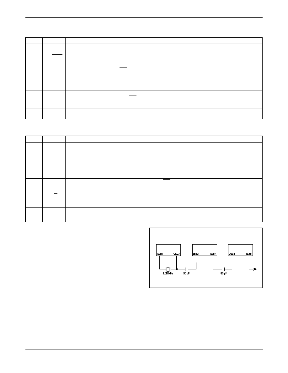
DTMF Clock Circuit
The internal clock circuit is completed with the addition of a stan-
dard 3.579545 MHz television color burst crystal. A number of
M-8880 devices can be connected as shown in Figure 8 using
only one crystal.
Microprocessor Interface
The M-8880 uses a microprocessor interface that allows pre-
cise control of transmitter and receiver functions. Five internal
registers are associated with the microprocessor interface,
which can be subdivided into three categories: data transfer,
transceiver control, and transceiver status. Two registers are
associated with data transfer operations. The receive data,
read-only, contains the output code of the last valid DTMF tone
pair to be decoded. The data entered in the transmit data regis-
ter determines which tone pair is to be generated (see Table 2).
Data can only be written to the transmit data register. Trans-
ceiver control is accomplished with two control registers (CRA
and CRB), occupying the same address space. A write opera-
tion to CRB can be executed by setting the appropriate bit in
CRA. The following write operation to the same address will
then be directed to CRB, and subsequent write cycles will then
be redirected to CRA. Internal reset circuitry clears the control
Page 5
M-8880
40-406-00012, Rev. G www.clare.com
Bit Name Function Description
b0 TOUT Tone output A logic 1 enables the tone output. This function can be implemented in either the burst mode or
nonburst mode.
b1 CP/DTMF
Mode control In DTMF mode (logic 0), the device is capable of generating and receiving DTMF signals. When
the call progress (CP) mode is selected (logic 1), a 6th-order bandpass filter is enabled to allow
call progress tones to be detected. Call progress tones within the specified bandwidth will be pre-
sented at the IRQ/CP pin in rectangular wave format if the IRQ bit has been enabled (b2 =1). Also,
when the CP mode and burst mode have both been selected, the transmitter will issue DTMF sig-
nals with a burst and pause of 102 ms (typ) duration. This signal duration is twice that obtained
from the DTMF transmitter, if DTMF mode had been selected. Note that DTMF signals cannot be
decoded when the CP mode has been selected.
b2 IRQ Interrupt enable A logic 1 enables the interrupt mode. When this mode is active and the DTMF mode has been se-
lected (b1 = 0), the IRQ/CP pin will pull to a logic 0 condition when either (1) a valid DTMF signal
has been received and has been present for the guard time or (2) the transmitter is ready for more
data (burst mode only).
b3 RSET Register select
A logic 1 selects control register B on the next write cycle to the control register address. Subse-
quent write cycles to the control register are directed back to control register A.
Table 4 Control Register A Description
Bit Name Function Description
b0 BURST
Burst mode A logic 0 enables the burst mode. When this mode is selected, data corresponding to the desired
DTMF tone pair can be written to the transmit data register, resulting in a tone burst of a specific
duration (see Table 12). Subsequently, a pause of the same duration is induced. Immediately fol-
lowing the pause, the status register is updated indicating that the transmit data register is ready
for further instructions, and an interrupt will be generated if the interrupt mode has been enabled.
Additionally, if call progress (CP) mode has been enabled, the burst and pause duration is increed
by a factor of two. When the burst mode is not selected (logic 1), tone bursts of any desired dura-
tion may be generated.
b1 TEST Test mode By enabling the test mode (logic 1), the IRQ/CP pin will present the delayed steering (inverted)
signal from the DTMF receiver. Refer to Figure 11 (b3 waveform) for details concerning the output
waveform. DTMF mode must be selected (CRA b1 = 0) before test mode can be implemented.
b2 S/D
Single/dual tone
generation
A logic 0 will allow DTMF signals to be produced. If single-tone generation is enabled (logic 1), ei-
ther now or column tones (low or high group) can be generated depending on the state of b3 in
control register B.
b3 C/R
Column/row
tones
When used in conjunction with b2 (above), the transmitter can be made to generate single-row or
single-column frequencies. A logic0 will select row frequencies and a logic 1 will select column fre-
quencies.
Table 5 Control Register B Description
Figure 8 Common Crystal Connection

registers on powerup; however, as a precautionary measure the
initialization software should include a routine to clear the regis-
ters. Refer to Tables 3 and 4 for details on the control registers.
The IRQ/CP pin can be programmed to provide an interrupt re-
quest signal on validation of DTMF signals, or when the trans-
mitter is ready for more data (burst mode only). The IRQ/CP pin
is configured as an open-drain output device and as such re-
quires a pullup resistor (see Figure 10).
Ordering Information
M-888001P 20-pin plastic DIP
M-8880-01SM 20-pin plastic SOIC
M-8880-01T 20-pin plastic SOIC,Tape and Reel
Page 6
M-8880
40-406-00012, Rev. G www.clare.com
RS0 R/W
Function
0 0 Write to transmitter
0 1 Read from receiver
1 0 Write to control register
1 1 Read from status register
Table 6 Internal Register Functions
Figure 9 Equations
b3 b2 b1 b0
RSEL IRQ CP/DTMF
TOUT
Table 7 CRA Bit Postions
b3 b2 b1 b0
C/R S/D TEST BURST
Table 8 CRB Bit Positions
Figure 10 Application Circuit (Single-Ended Input)

Page 7
M-8880
40-406-00012, Rev. G www.clare.com
Parameter Symbol Min Typ* Max Units
Operating supply voltage V
DD
4.75 5.0 5.25 V
Operating supply current I
DD
--
10
15
mA
Power consumption P
O
-- 50 78.75 mW
Inputs
High-level input voltage, OSC1 V
IHO
3.5 -- -- V
Low-level input voltage, OSC1 V
ILO
-- -- 1.5 V
Input impedance (@ 1 kHz), IN+, IN- R
IN
--
10
--
M
Steering threshold voltage V
TSt
2.2 2.3 2.5 V
Outputs
High-level output voltage (no load), OSC2 V
OHO
V
DD
- 0.1V -- -- V
Low-level output voltage (no load), OSC2 V
OLO
-- -- 0.1 V
Output leakage current (V
OH
= 2.4V), IRQ I
OZ
-- 1.0 10.0
µ
A
V
REF
output voltage (no load) V
REF
2.4 -- 2.7 V
V
REF
output resistance R
OR
-- 1.0 k
Data Bus
Low-level input voltage V
IL
-- -- 0.8 V
High-level input voltage V
IH
2.0 -- -- V
Low-level output voltage (I
OL
= 1.6 mA) V
OL
-- -- 0.4 V
High-level output voltage (I
OH
= 400
µ
A) V
OH
2.4 -- -- V
Input leakage current (V
IN
= 0.4 to 2.4 V) I
IZ
-- -- 10.0
µ
A
All voltages referenced to V
SS
unless otherwise noted. V
DD
= 5.0 V
±
5%; f
C
= 3.579545 MHz;
A
= -40∞C to +85
∞
C, unless otherwise
noted. *Typical values are for use as design aids only, and are not guaranteed or subject to production testing.
Table 11 DC Characteristics
BIT Name Status Flag Set Status Flag Cleared
b0 IRQ Interrupt has occurred. Bi tone (b1) and/or bit 2 (b2)
is set.
Interrupt is inactive. Cleared after status register is
read.
b1 Transmit data register
empty (burst mode only)
Pause duration has terminated and transmitter is
ready for new data.
Cleared after status register is read or when not in
burst mode.
b2 Receive data register
full
Valid data is in the receive data register. Cleared after status register is read.
b3 Delayed steering
Set on valid detection of the absence of a DTMF sig-
nal.
Cleared on detection of a valid DTMF signal.
Table 9 Status Register Description
Parameter Symbol Value
Power supply voltage (V
DD
- V
SS
) V
DD
+ 6.0 V max
Voltage on any pin V
dc
V
SS
-0.3 V to V
DD
+ 0.3 V
Current on any pin I
DD
10 mA max
Operating temperature T
A
-40∞C to +85∞C
Storage temperature T
S
-65∞C to +150∞C
Note: Exceeding these ratings may cause permanent damage. Functional operation under these conditions is not implied.
Table 10 Absolute Maximum Ratings

M-8880
40-406-00012, Rev. G www.clare.com
Page 8
PARAMETER SYMBOL MIN TYP* MAX UNITS
Receive signal conditions
Valid input signal levels
(each tone of composite signal; Notes 1, 2, 3, 5, 6, 9)
-29
27.5
--
--
+1
869
dBm
mV
RMS
Positive twist accept (Notes 2, 3, 6, 9) --
6
dB
Negative twist accept (Notes 2, 3, 6, 9) --
6
dB
Frequency deviation accept (Notes 2, 3, 5, 9) ± 1.5% ± 2 Hz -- -- Nom.
Frequency deviation reject (Notes 2, 3, 5)
±
3.5% -- -- Nom.
Third tone tolerance (Notes 2, 3, 4, 5, 9, 10) -- -16 -- dB
Noise tolerance (Notes 2, 3, 4, 5, 7, 9, 10) -- -12 -- dB
Dial tone tolerance (Notes 2, 3, 4, 5, 8, 9, 11) -- +22 -- dB
Call progress
Lower frequency (@ -25 dBm) accept f
LA
-- 320 -- Hz
Upper frequency (@ -25 dBm) accept f
HA
-- 510 -- Hz
Lower frequency (@ -25 dBm) reject f
LR
-- 290 -- Hz
Upper frequency (@ -25 dBm) reject f
HR
-- 540 -- Hz
Receive timing
Tone present detect time t
DP
5
11
14
ms
Tone absent detect time t
DA
0.5 4 8.5 ms
Tone duration accept (ref. Figure 12) t
REC
-- -- 40 ms
Tone duration reject (ref. Figure 12) t
REC
20 -- -- ms
Interdigit pause accept (ref. Figure 12) t
ID
-- -- 40 ms
Interdigit pause reject (ref. Figure 12) t
DO
20 -- -- ms
Delay St to b3 t
PStb3
--
13
--
µ
s
Delay St to RX
O
--RX
3
t
PStRX
--
8
--
µ
s
Transmit timing
Tone burst duration (DTMF mode) t
BST
50 -- 52 ms
Tone pause duration (DTMF mode) t
PS
50 -- 52 ms
Tone burst duration (extended, call progress mode) t
BSTE
100 -- 104 ms
Tone pause duration (extended, call progress mode) t
PSE
100 -- 104 ms
Tone output
High group output level (R
L
= 10 k
) V
HOUT
-6.1 -- -2.1 dBm
Low group output level (R
L
= 10 k
W
) V
LOUT
-8.1 -- -4.1 dBm
Pre-emphasis (R
L
= 10 k
W
) dB
P
0
2
3
dB
Output distortion (R
L
= 10 k
, 3.4 kHz bandwidth) THD -- -25 -- dB
Frequency deviation (f = 3.5795 MHz) f
D
-- ± 0.7 ± 1.5 %
Output load resistance R
LT
10 -- 50 k
Microprocessor interface
2 cycle period t
CYC
0.5 -- --
µ
s
2 high pulse width t
CH
200 -- -- ns
2 low pulse width t
CL
180 -- ns
2 rise and fall time t
R
, t
F
-- -- 25 ns
Address, R/W hold time t
AH
, t
RWH
10 -- -- ns
Address, R/W setup time (prior to
2) t
AS
, t
RWS
23 -- -- ns
Table 12 AC Characteristics

Page 9
M-8880
40-406-00012, Rev. G www.clare.com
Parameter Symbol Min Typ* Max Units
Microprocessor interface (continued)
Data hold time (read) t
DHR
22 -- -- ns
f
2 to valid data delay (read) (200 pF load) t
DDR
-- -- 150 ns
Data setup time (write) t
DSW
45 -- -- ns
Data hold time (write) t
DHW
10 -- -- ns
Input capacitance, D0--D3 C
IN
--
5
--
pF
Output capacitance, IRQ/CP C/
OUT
--
5
--
pF
DTMF clock
Crystal clock frequency f
C
3.5759 3.5795 3.5831 MHz
Clock input rise time (external clock) t
LHCL
-- -- 110 ns
Clock input fall time (external clock) t
HLCL
-- -- 110 ns
Clock input duty cycle (external clock) DC
CL
40 50 60 %
Capacitive load, OSC2 C
LO
-- -- 30 pF
All voltages referenced to unless otherwise noted. V
DD
= 5.0 V
±
5%; V
SS
= 0 V; f
C
= 3.579545 MHz; T
A
= -40
∞
C to +85
∞
C
*Typical values are for use as design aids only, and are not guaranteed or subject to production testing.
Notes:
1. dBm = decibels above or below a reference power of 1 mW into a 600
W
load.
2. Digit sequence consists of all 16 DTMF tones.
3. Tone duration = 40 ms. Tone pause = 40 ms.
4. Nominal DTMF frequencies are used.
5. Both tones in the composite signal have an equal amplitude.
6. The tone pair is deviated by
±
1.5%
±
2 Hz.
7. Bandwidth limited (3 kHz) Gaussian noise.
8. The precise dial tone frequencies are 350 and 440 Hz (
±
2%).
9. For an error rate of less than 1 in 10,000.
10. Referenced to the lowest amplitude tone in the DTMF signal.
11. Referenced to the minimum valid accept level.
Table 12 AC Characteristics (continued)
Parameter Symbol Min Typ* Max Units
Input leakage current (V
SS
£
V
IN
£
V
DD
) I
IN
-- 100 -- nA
Input resistance R
IN
--
10
--
M
Input offset voltage V
OS
--
25
--
mV
Power supply rejection (1 KHz) PSRR -- 60 -- dB
Common mode rejection (-3.0 V
£
V
IN
£
3.0 V
)
CMRR -- 60 -- dB
DC open-loop voltage gain A
VOL
--
65
--
dB
Unity gain bandwidth BW -- 1.5 -- MHz
Output voltage swing (R
L
≥
100 K
to V
SS
) V
O
-- 4.5 -- V
PP
Maximum capacitive load, GS C
L
-- 100 -- pF
Maximum resistive load, GS R
L
--
50
--
K
Common mode range (no load) V
CM
-- 3.0 -- V
PP
All voltages referenced to unless otherwise noted. V
DD
= 5.0 V; V
SS
= 0 V; T
A
= 25
∞
C
*Typical values are for use as design aids only, and are not guaranteed or subject to production testing.
Table 13 Electrical Characteristics - Gain Setting Amplifier

Page 10
M-8880
40-406-00012, Rev. G www.clare.com
Figure 11 Timing Diagrams
Figure 12 Test Loads

Page 11
M-8880
40-406-00012, Rev. G www.clare.com
Explanation of Events
(A) Tone bursts detected, tone duration invalid, RX Data Register not updated.
(B) Tone #n detected, tone duration valid, tone decoded and latched in RX Data Register.
(C) End of tone #n detected, tone absent duration valid, RX Data Register remain latched until next valid tone.
(D) Tone #n + 1 detected, tone duration valid, tone decoded and latched in RX Data Register.
(E) Acceptable dropout of tone #n + 1, tone absent duration invalid, RX Data Register remain latched.
(F) End of tone #n + 1 detected, tone absent duration valid, RX Data Register remain latched until next valid tone.
Explanation of Symbols
V
IN
DTMF composite input signal.
ESt Early steering output. Indicates detection of valid tone frequencies.
St/GT Steering input/guard time output. Drives external RC timing circuit.
RX
0
-RX
3
4-bit decoded data in receive data register.
b3 Delayed steering output. Indicates that valid frequencies have been present/absent for the
required guard time, thus constituting a valid DTMF signal.
b2 Output enable (input). A low level shifts Q1 - Q4 to its high impedance state.
IRQ/CP Interrupt is active indicating that new data is in the RX data register. The interrupt is cleared
after the status register is ready.
t
REC
Maximum DTMF signal duration not detected as valid.
t
REC
Minimum DTMF signal duration required for valid recognition.
t
ID
Minimum time between valid DTMF signals.
t
DO
Maximum allowable dropout during valid DTMF signal.
t
DP
Time to detect the presence of valid DTMF signals.
t
DA
Time to detect the absence of valid DTMF signals.
T
GTP
Guard time, tone present.
t
GTA
Guard time, tone absent.
Figure 13 Timing Diagrams

Page 12
M-8880
40-406-00012, Rev. G www.clare.com
Figure 14 Package Dimensions
Tolerances
Inches Metric (mm)
Min Max Min Max
A .093 .104 2.35 2.65
A1 .004 .012 .10 .30
b .013 .020 .33 .51
D .496 .512 12.60 13.00
E .291 .299 7.39 7.59
e .050 BSC 1.27 BSC
H .394 .419 10.00 10.65
L .016 .050 .40 1.27
Tolerances
Inches Metric (mm)
Min Max Min Max
A .210 5.33
A1 .015 .38
b .014 .022 .36 .56
b
2
.045 .070 1.14 1.78
C .008 .014 .20 .36
D .980 1.060 24.89 26.92
E .300 .325 7.62 8.26
E1 .240 .280 6.10 7.11
e .100 BSC 2.54 BSC
e
c
0
∞
15∞ 0∞ 15∞
L .115 .150 2.92 3.81

Worldwide Sales Offices
CLARE LOCATIONS
Clare Headquarters
78 Cherry Hill Drive
Beverly, MA 01915
Tel: 1-978-524-6700
Fax: 1-978-524-4900
Toll Free: 1-800-27-CLARE
Clare Micronix Division
145 Columbia
Aliso Viejo, CA 92656-1490
Tel: 1-949-831-4622
Fax: 1-949-831-4628
SALES OFFICES
AMERICAS
Americas Headquarters
Clare
78 Cherry Hill Drive
Beverly, MA 01915
Tel: 1-978-524-6700
Fax: 1-978-524-4900
Toll Free: 1-800-27-CLARE
Eastern Region
Clare
P.O. Box 856
Mahwah, NJ 07430
Tel: 1-201-236-0101
Fax: 1-201-236-8685
Toll Free: 1-800-27-CLARE
Central Region
Clare Canada Ltd.
3425 Harvester Road, Suite 202
Burlington, Ontario L7N 3N1
Tel: 1-905-333-9066
Fax: 1-905-333-1824
Northwestern Region
Clare
1852 West 11th Street, #348
Tracy, CA 95376
Tel: 1-209-832-4367
Fax: 1-209-832-4732
Toll Free: 1-800-27-CLARE
Southwestern Region
Clare
2816 Nevis Circle
Costa Mesa, CA 92626
Tel: 1-714-556-3661
Fax: 1-714-546-4254
Toll Free: 1-800-27-CLARE
Canada
Clare Canada Ltd.
3425 Harvester Road, Suite 202
Burlington, Ontario L7N 3N1
Tel: 1-905-333-9066
Fax: 1-905-333-1824
EUROPE
European Headquarters
CP Clare nv
Bampslaan 17
B-3500 Hasselt (Belgium)
Tel: 32-11-300868
Fax: 32-11-300890
France
Clare France Sales
Lead Rep
99 route de Versailles
91160 Champlan
France
Tel: 33 1 69 79 93 50
Fax: 33 1 69 79 93 59
Germany
Clare Germany Sales
ActiveComp Electronic GmbH
Mitterstrasse 12
85077 Manching
Germany
Tel: 49 8459 3214 10
Fax: 49 8459 3214 29
Italy
C.L.A.R.E.s.a.s.
Via C. Colombo 10/A
I-20066 Melzo (Milano)
Tel: 39-02-95737160
Fax: 39-02-95738829
Sweden
Clare Sales
Comptronic AB
Box 167
S-16329 SpÂnga
Tel: 46-862-10370
Fax: 46-862-10371
United Kingdom
Clare UK Sales
Marco Polo House
Cook Way
Bindon Road
Taunton
UK-Somerset TA2 6BG
Tel: 44-1-823 352541
Fax: 44-1-823 352797
Specification: 40-406-00012, Rev. G
© Copyright 2000, CP Clare Corporation d/b/a Clare
All rights reserved. Printed in USA.
07/28/00
Clare cannot assume responsibility for use of any circuitry other then cir-
cuitry entirely embodied in this Clare product. No circuit patent licenses nor
indemnity are expressed or implied. Clare reserves the right to change the
specification and circuitry, without notice at an y time.
The products de-
scribed in this document are not intended for use in medical implantation
or other direct life support applications where malfunction may result in
direct physical harm, injury or death to a person.
ASIA PACIFIC
Asian Headquarters
Clare
Room N1016, Chia-Hsin, Bldg II,
10F, No. 96, Sec. 2
Chung Shan North Road
Taipei, Taiwan R.O.C.
Tel: 886-2-2523-6368
Fax: 886-2-2523-6369
http://www.clare.com