1
www.clare.com
M-88L70
DS-M88L70-R1
The M-88L70 monolithic DTMF receiver offers small size,
low power consumption and high performance, with 3 volt
operation. Its architecture consists of a bandsplit filter
section, which separates the high and low group tones,
followed by a digital counting section which verifies the
frequency and duration of the received tones before
passing the corresponding code to the output bus.
∑
Telephone switch equipment
∑
Mobile radio
∑
Remote control
∑
Paging systems
∑
PCMCIA
∑
Portable TAD
∑
Remote data entry
∑
Operates between 2.7 and 3.6 volts
∑
Low power consumption
∑
Power-down mode
∑
Inhibit mode
∑
Central office quality and performance
∑
Inexpensive 3.58 MHz time base
∑
Adjustable acquisition and release times
∑
Dial tone suppression
∑
Functionally compatible with Clare's M-8870
Applications
Features
Description
3V DTMF Receiver
Ordering Information
Part #
Description
M-88L70-01P
18-pin plastic DIP
M-88L70-01S 18-pin
SOIC
M-88L70-01T
18-pin SOIC, Tape and Reel
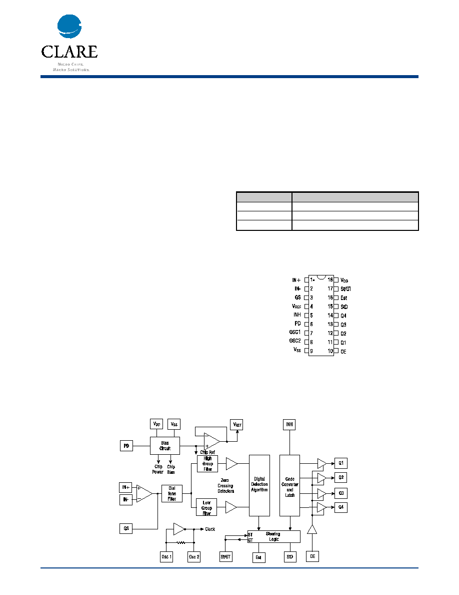
Figure 2 Block Diagram
Figure 1 Pin Connections
The M-88L70 is a full DTMF Receiver that integrates
both bandsplit filter and decoder functions into a single
18-pin DIP or SOIC package. Manufactured using
CMOS process technology, the M-88L70 offers low
power consumption (18 mW max), precise data handling
and 3V operation. Its filter section uses switched capaci-
tor technology for both the high and low group filters and
for dial tone rejection. Its decoder uses digital counting
techniques to detect and decode all 16 DTMF tone pairs
into a 4-bit code. External component count is minimized
by provision of an on-chip differential input amplifier,
clock generator, and latched tri-state interface bus.
Minimal external components required include a low-cost
3.579545 MHz color burst crystal, a timing resistor, and a
timing capacitor.
www.clare.com
M-88L70
Rev. 1
2
Filter
The low and high group tones are separated by applying
the dual-tone signal to the inputs of two 9th order
switched capacitor bandpass filters with bandwidths that
correspond to the bands enclosing the low and high
group tones. The filter also incorporates notches at 350
and 440 Hz, providing excellent dial tone rejection. Each
filter output is followed by a single-order switched capac-
itor section that smoothes the signals prior to limiting.
Signal limiting is performed by high-gain comparators
provided with hysteresis to prevent detection of unwant-
ed low-level signals and noise. The comparator outputs
provide full-rail logic swings at the frequencies of the
incoming tones.
Decoder
The M-88L70 decoder uses a digital counting technique
to determine the frequencies of the limited tones and to
verify that they correspond to standard DTMF frequen-
cies. A complex averaging algorithm is used to protect
against tone simulation by extraneous signals (such as
voice) while tolerating small frequency variations. The
algorithm ensures an optimum combination of immunity
to talkoff and tolerance to interfering signals (third tones)
and noise. When the detector recognizes the simultane-
ous presence of two valid tones (known as "signal condi-
tion"), it raises the Early Steering flag (ESt). Any subse-
quent loss of signal condition will cause ESt to fall.
Steering Circuit
Before a decoded tone pair is registered, the receiver
checks for a valid signal duration (referred to as "char-
acter-recognition-condition"). This check is performed
by an external RC time constant driven by ESt. A logic
high on ESt causes V
C
(see Figure 3) to rise as the
capacitor discharges. Provided that signal condition is
maintained (ESt remains high) for the validation period
(t
GTP
), VC reaches the threshold (V
TSt
) of the steering
logic to register the tone pair, thus latching its corre-
sponding 4-bit code (see Table 2) into the output latch.
At this point, the GT output is activated and drives V
C
to
V
DD
. GT continues to drive high as long as ESt remains
high. Finally, after a short delay to allow the output latch
to settle, the "delayed steering" output flag (StD) goes
high, signaling that a received tone pair has been reg-
istered. The contents of the output latch are made
available on the 4-bit output bus by raising the three-
state control input (OE) to a logic high. The steering cir-
cuit works in reverse to validate the interdigit pause
between signals. Thus, as well as rejecting signals too
short to be considered valid, the receiver will tolerate
signal interruptions (dropouts) too short to be consid-
Table 1 Pin Functions
Pin
Name
Description
1
IN+
Non-inverting input
2
IN
-Inverting input
3
GS
Gain select. Gives access to output of front-end amplifier for connection of feedback resistor.
4
V
REF
Reference voltage output (nominally V
DD
/2). May be used to bias the inputs at mid-rail.
5
INH
Inhibits detection of tones representing keys A, B, C, and D. This input is internally pulled down.
6
PD
Power down. Logic high powers down the device and inhibits the oscillator. This input is internally pulled down.
7
OSC1
Clock input
8
OSC2
Clock output
9
V
SS
Negative power supply (normally connected to 0 V).
10
OE
Tri-state output enable (input). Logic high enables the outputs Q1 - Q4. Internal pullup.
11-14
Q1, Q2,
Tri-state outputs. When enabled by OE, provides the code corresponding to the last valid tone pair received
Q3, Q4
(see Table 5.)
15
StD
Delayed steering output. Presents a logic high when a received tone pair has been registered and the output latch is
updated. Returns to logic low when the voltage on St/GT falls below V
TSt
16
ESt
Early steering output. Presents a logic high immediately when the digital algorithm detects a recognizable tone pair
(signal condition). Any momentary loss of signal condition will cause ESt to return to a logic low.
17
St/GT
Steering input/guard time output (bidirectional). A voltage greater than V
TSt
detected at St causes the device to
register the detected tone pair and update the output latch. A voltage less than V
TSt
frees the device to accept a new
tone pair. The GT output acts to reset the external steering time constant, and its state is a function of ESt and the
voltage on St. (See Figure 5).
18
V
DD
Positive power supply
Connections to the front-end differential amplifier
3.579545 MHz crystal connected between these pins completes internal oscillator.

M-88L70
www.clare.com
Rev. 1
3
ered a valid pause. This capability, together with the
ability to select the steering time constants externally,
allows the designer to tailor performance to meet a wide
variety of system requirements.
Guard Time Adjustment
Where independent selection of receive and pause are
not required, the simple steering circuit of Figure 3 is
applicable. Component values are chosen according to
the formula:
t
REC
= t
DP
+ t
GTP
t
GTP
@ 0.67 RC
The value of t
DP
is a parameter of the device and t
REC
is
the minimum signal duration to be recognized by the
receiver. A value for C of 0.1
µ
F is recommended for
most applications, leaving R to be selected by the
designer. For example, a suitable value of R for a t
REC
of
40 ms would be 300 K ohm. A typical circuit using this
steering configuration is shown in Figure 4. The timing
requirements for most telecommunication applications
are satisfied with this circuit. Different steering arrange-
ments may be used to select independently the guard
times for tone-present (t
GTP
) and tone-absent (t
GTA
). This
may be necessary to meet system specifications that
place both accept and reject limits on both tone duration
and interdigit pause.
Guard time adjustment also allows the designer to tailor
system parameters such as talkoff and noise immunity.
Increasing t
REC
improves talkoff performance, since it
reduces the probability that tones simulated by speech
will maintain signal condition long enough to be regis-
tered. On the other hand, a relatively short t
REC
with a
long t
DO
would be appropriate for extremely noisy envi-
ronments where fast acquisition time and immunity to
dropouts would be required. Design information for
guard time adjustment is shown in Figure 5.
Input Configuration
The input arrangement of the M-88L70 provides a dif-
ferential input operational amplifier as well as a bias
source (V
REF
) to bias the inputs at mid-rail. Provision is
made for connection of a feedback resistor to the op-
amp output (GS) for gain adjustment.
In a single-ended configuration, the input pins are con-
nected as shown in Figure 4 with the op-amp connect-
ed for unity gain and V
REF
biasing the input at 1/2V
DD
.
Figure 7 shows the differential configuration, which per-
mits gain adjustment with the feedback resistor R5.
Figure 3 Basic Steering Circuit
F
LOW
F
HIGH
Key OE
INH
ESt
Q4
Q3
Q2
Q1
(ref.)
ANY
ANY
ANY
L
X
H
Z
Z
Z
Z
697
1209
1
H
X
H
0
0
0
1
697
1336
2
H
X
H
0
0
1
0
697
1477
3
H
X
H
0
0
1
1
770
1209
4
H
X
H
0
1
0
0
770
1336
5
H
X
H
0
1
0
1
770
1477
6
H
X
H
0
1
1
0
852
1209
7
H
X
H
0
1
1
1
852
1336
8
H
X
H
1
0
0
0
852
1477
9
H
X
H
1
0
0
1
941
1336
0
H
X
H
1
0
1
0
941
1209
*
H
X
H
1
0
1
1
941
1477
#
H
X
H
1
1
0
0
697
1633
A
H
L
H
1
1
0
1
770
1633
B
H
L
H
1
1
1
0
852
1633
C
H
L
H
1
1
1
1
941
1633
D
H
L
H
0
0
0
0
697
1633
A
H
H
L Undetected, the output
770
1633
B
H
H
L code will remain the
852
1633
C
H
H
L same as the previous
941
1633
D
D
H
L
detected code.
L = logic low, H = logic high, Z = high impedance, X = don't care
Table 2 Tone Decoding

www.clare.com
4
M-88L70
Rev. 1
Parameter
Symbol
Value
Power supply voltage
V
DD
6.0 V max
(V
DD
- V
SS
)
Voltage on any pin
V
dc
V
SS
-0.3 Min,
V
DD
+0.3 Max
Current on any pin
I
DD
10 mA max
Operating temperature
T
A
-40∞C to + 85∞C
Storage temperature
T
S
-65∞C to + 150∞C
Note:
Exceeding these ratings may cause permanent damage. Functional operation under these condi-
tions is not implied.
Table 4 DC Characteristics
PARAMETER
SYMBOL
MIN
TYP
MAX
UNITS
TEST CONDITIONS
Operating supply voltage
V
DD
2.7
3.0
3.6
V
Operating supply current
I
DD
-
3.0
5.0
mA
Standby supply current
I
DDS
-
5.0
10
µ
A
PD=V
DD
Power consumption
P
O
-
9
18
mW
Low level input voltage
V
IL
-v
-
1.0
V
V
DD
= 3.0 V
High level input voltage
V
IH
2
-
-
V
V
DD
= 3.0 V
Input leakage current
I
IH
/I
IL
-
0.1
-
µ
A
V
IN
= V
SS
or V
DD
(see Note 2)
Pullup (source) current on OE
I
SO
-12
-
-
µ
A
OE = 0 V
Pull down (sink) Curent PD
I
PD
-
1.0
45
µ
A
PD = 3.0 V
Pull down (sink) Current INH
I
INH
-
1.0
45
µ
A
INH = 3.0 V
Input impedance, signal inputs 1, 2
R
IN
-
10
-
M
@ 1 kHz
Steering threshold voltage
V
TSt
-
1.5
-
V
Low level output voltage
V
OL
-
0.1
0.4
V
I
OL
= 1.0 mA
High level output voltage
V
OH
2.4
2.6
-
V
I
OH
= -400 mA
Output high (source) current
I
OH
1.0
-
mA
V
OUT
= 2.5 V @ V
DD
= 2.7 V
Output voltage V
REF
V
REF
-
1.5
-
V
No load
Output resistance V
REF
R
OR
-
10
-
k
Notes:
1. All voltages referenced to V
SS
unless otherwise noted. For typical values, V
DD
= 3.0 V + 20%/-10%, V
SS
= 0 V, T
A
= 25∞C
2. Input pins defined as IN+, IN-, and OE.
Absolute Maximum Ratings are stress ratings. Stresses
in excess of these ratings can cause permanent dam-
age to the device. Functional operation of the device at
these or any other conditions beyond those indicated in
the operational sections of this data sheet is not implied.
Exposure of the device to the absolute maximum ratings
for an extended period may degrade the device and
effect its reliability.
Absolute Maximum Ratings

M-88L70
www.clare.com
5
Rev. 1
Table 5 Operating Characteristics - Gain Setting Amplifier
PARAMETER
SYMBOL
MIN
TYP
MAX
UNITS
TEST CONDITIONS
Input leakage current
I
N
-
100
-
nA
V
SS
< V
IN
< V
DD
Input resistance
R
IN
-
10
-
M
Input offset voltage
V
OS
-
15
25
mV
Power supply rejection
PSRR
50
60
-
dB
1 kHz
Common mode rejection
CMRR
40
60
-
dB
-3.0V < V
IN
< 3.0V
DC open loop voltage gain
A
VOL
32
65
-
dB
Open loop unity gain bandwidth
f
C
0.3
1.0
-
MHz
Output voltage swing
V
O
-
2.2
-
V
P-P
RL 3 100 k
to V
SS
Tolerable capacitive load (GS)
C
L
-
-
100
pF
Tolerable resistive load (GS)
R
L
50
-
-
k
Common mode range
V
CM
-
1.5
-
V
P-P
No load
All voltages referenced to V
SS
unless otherwise noted. V
DD
= 3.0 V +20%/-10%, V
SS
= 0 V, TA = -40∞C to + +85∞C
Table 6 AC Characteristics
PARAMETER
SYMBOL
MIN
TYP
MAX
UNITS
NOTES
Valid input signal levels
-
-36
-
-6.4
dBm
1,2,3,4,5,8
(each tone of composite signal)
-
12.3
-
370
mVRMS
Positive twist accept
-
-
-
6
dB
Negative twist accept
-
-
-
6
dB
Frequency deviation accept limit
-
-
-
1.5% ±2 Hz
Nom.
2,3,5,8,10
Frequency deviation reject limit
-
±3.5%
-
-
Nom.
2,3,5
Third tone tolerance
-
-
-16
-
dB
2,3,4,5,8,9,13,14
Noise tolerance
-
-
-12
-
dB
2,3,4,5,6,8,9
Dial tone tolerance
-
-
+22
-
dB
2,3,4,5,7,8,9
Tone present detection time
t
DP
5
8
14
ms
See Figure 8
Tone absent detection time
t
DA
0.5
3
8.5
ms
Minimum tone duration accept
t
REC
-
40
ms
User adjustable (see Figures 3
Maximum tone duration reject
t
REC
20
-
-
ms
and Figure 5)
Minimum interdigit pause accept
t
ID
-
-
40
ms
Maximum interdigit pause reject
t
DO
20
-
-
ms
Propagation delay (St to Q)
t
PQ
-
13
-
µ
s
OE = V
DD
Propagation delay (St to StD)
t
PStD
-
8
-
µ
s
Output data setup (Q to StD)
t
QStD
-
3.4
-
µ
s
Propagation delay (OE to Q), enable
t
PTE
-
200
-
ns
R
L
= 10k
, CL = 50 pF
Propagation delay (OE to Q), disable
t
PTD
-
500
-
ns
Crystal clock frequency
f
CLK
3.5759
3.5795
3.5831
MHz
Clock output (OSC2), capacitive load
C
LO
-
-
30
pF
All voltages referenced to VSS unless otherwise noted. For typical values V
DD
= 3.0 V, V
SS
= 0 V, T
A
= -40∞C to +85∞C, f
CLK
= 3.579545 MHz. Notes:
1. dBm = decibels above or below a reference power of 1 mW into a 600
load.
2. Digit sequence consists of all 16 DTMF tones.
3. Tone duration = 40 ms. Tone pause = 40 ms.
4. Nominal DTMF frequencies are used, measured at GS.
5. Both tones in the composite signal have an equal amplitude.
6. Bandwidth limited (0 to 3 kHz) Gaussian noise.
7. The precise dial tone frequencies are (350 and 440 Hz) ± 2%.
8. For an error rate of better than 1 in 10,000.
9. Referenced to lowest level frequency component in DTMF signal.
10. Minimum signal acceptance level is measured with specified maximum frequency deviation.
11. Input pins defined as IN+, IN-, and OE.
12. External voltage source used to bias VREF.
13. This parameter also applies to a third tone injected onto the power supply.
14. Referenced to Figure 4. Input DTMF tone level at -28 dBm.