
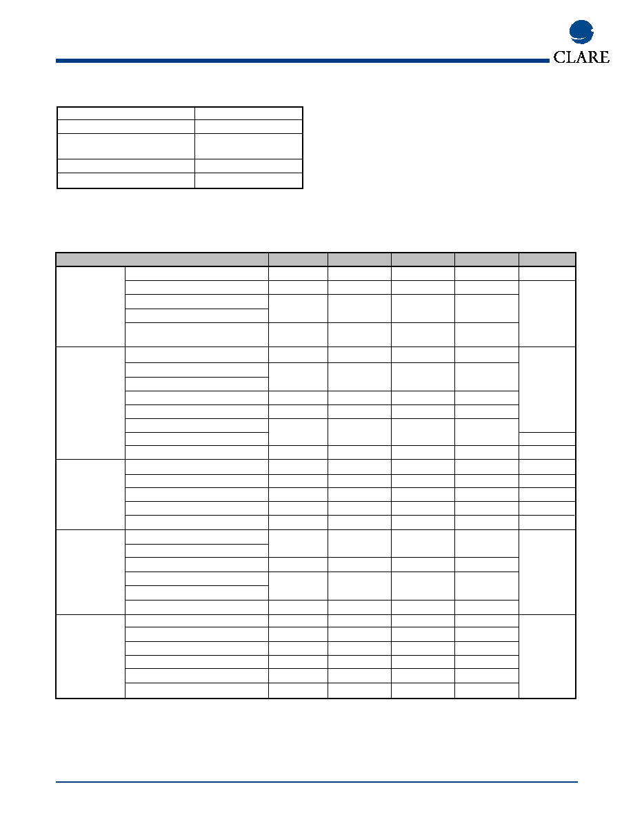
Part #
Description
M-991
14-pin plastic DIP
M-991-01SM
16-pin SOIC
M-991-01SMTR
16-pin SOIC Tape and Reel
M-991-02SM
16-pin SOIC, Extended
Temperature Range
M-991-02SMTR
16-pin SOIC, Extended
Temperature Range, Tape and
Reel
www.clare.com
DS-M991-R1
M-991
Call Progress Tone Generator
1
Block Diagram
Pin Assignments
Ordering Information
Features
∑
Generates standard call progress tones
∑
Digital input control
∑
Linear (analog) output
∑
Power output capable of driving standard line
∑
14-pin DIP and 16-pin SOIC package types
∑
Single supply 5V CMOS (low power)
∑
Inexpensive 3.58 MHz time base
∑
Temperature range from -25∫C to 70∫C (-01 ver-
sion)
∑
Temperature range from -40∫C to 85∫C (-02 ver-
sion)
Applications
∑
Telephone systems
∑
Test equipment
∑
Callback
∑
Security systems
∑
Billing systems
Description
The M-991 is a call progress tone generator integrated
circuit for use in telephone systems. The circuit uses
low-power CMOS techniques to generate tones which
are digitally controlled and highly linear. The M-991 is
designed to permit operation with almost any system.
The use of integrated circuit techniques allows the M-
991 to incorporate the control, tone generating, and
power output buffer into a single 14-pin DIP or a 16-pin
SOIC. A 3.58-MHz (color burst) crystal-controlled time
base guarantees accuracy and repeatability.
Absolute Maximum Ratings
Storage Temperature
-55∞ to 125∞ C
Operating Ambient Temperature
-25∞ to 70∞ C
Operating Ambient Temperature
-40∞ to 85∞ C
for the M-991-02SM
V
DD
7.0V
Any Input Voltage
V
SS
-0.6 to V
DD
+0.6V
Note:
1. Exceeding these ratings may permanently damage the M-991.
www.clare.com
2
M-991
Rev. 1
7. At XOUT pin as compared to 3.579545 MHz.
8. OUTDRIVE with load >5 KW/OUTDRIVE with
540 W load.
9. Resistance at V
REF
to V
DD
or V
SS
> 1 MW.
10. Crystal oscillator active.
11. Measured 90% to 10%.
Absolute Maximum Ratings are stress ratings. Stresses in
excess of these ratings can cause permanent damage to
the device. Functional operation of the device at these or
any other conditions beyond those indicated in the opera-
tional sections of this data sheet is not implied. Exposure of
the device to the absolute maximum ratings for an extend-
ed period may degrade the device and effect its reliability.
Specifications
Parameter
Min
Typ
Max
Units
Notes
Power Supply
V
DD
4.75
-
5.25
V
1
and Reference
Current Drain, IDD
-
2.0/4.0
-
mA
8
V
REF
Pin:
Deviation from (V
DD
+ V
SS
)/2
-2
-
+2
%
Internal Resistance from V
REF
3.25
-
6.75
k
to V
DD
, V
SS
Oscillator
Frequency Deviation
-0.01
-
+0.01
%
7
External Clock: (XOUT open)
V
IL
0
-
0.2
V
V
IH
V
DD
- 0.2
-
V
DD
V
Duty Cycle
40
-
60
%
XIN, XOUT Loading:
Capacitance
-
-
10
pF
10
Resistance
20
-
-
M
-
Tone Output
Frequency Deviation
-0.5
-
+0.5
%
-
Level
100
-
180
mV
2
Distorting Components
-35
-
-
dB
3
Idle
-
-
-60
dBm
4
OUTDRIVE Envelope Rise Time
-
-
4
ms
5
Control
DX, CE Pns:
V
IL
-
-
0.5
V
6
V
IH
2.5
-
-
V
Mute Pins:
VOL (I
SINK
= -100 µA)
-
-
1.5
V
V
OH
(I
SOURCE
= 100 µA)
V
DD
- 1.5
-
-
V
Timing
Data Setup (t
DS
)
200
-
-
ns
11
Data Hold (t
DH
)
10
-
-
ns
Chip Enable Fall (t
PL
)
-
-
90
ns
Tone On Delay (t
TO
)
-
-
5
ms
Tone Off Delay (t
TD
)
-
-
5
ms
Mute Delay from Outdrive (t
MO
)
-
-
200
ns
Notes: (unless otherwise specified)
1. All DC voltages are referenced to V
SS
.
2. Vrms per tone, 540 W load.
3. Any one frequency relative to the lowest level output tone (f<4000 Hz).
4. 0 dBm = 0.775 Vrms.
5. To 90% maximum amplitude.
6. For all supply voltages in the operating range.

Data/Tone Selection
D0
D1
D2 D3 Frequency (Hz)
Use
1
2
0
0
0
0
350
440
Dial Tone
0 0
0
1
400
off
Special
0
0
1
0
440
off
Alert Tone
0
0
1
1
440
480
Audible Ring
0
1
0
0
440
620
Pre-empt
0
1
0
1
480
off
Bell high tone
0
1
1
0
480
620
Reorder(Bell low)
0
1
1
1
350
off
Special
1
0
0
0
620
off
Special
1
0
0
1
941
1209
DTMF "
*
"
Pin Function
Pin
Function
CE
Latches data and enables output (active
low input).
D0 - D3
Data input pins. (See Data/Tone Selection.)
D4-D5
Leave open.
MUTE
Output indicates that a signal is being generated at
OUTDRIVE.
OUTDRIVE
Linear buffered tone output.
V
DD
Most positive power supply input pin.
V
REF
Internally generated mid-power supply voltage
(output).
V
SS
Most negative power supply input pin.
X
IN
Crystal oscillator or digital clock input.
X
OUT
Crystal oscillator output.
M-991
www.clare.com
3
Rev. 1
Call Progress Tone Generation
Call progress tones are audible tones sent from
switching systems to calling parties (or equipment) to
indicate the status of calls. Calling parties can identify
the success of a placed call by what is heard after dial-
ing. The M-991 series utilizes a highly linear tone gen-
erator that produces the unique frequencies (singly or
in pairs) that are common to call progress signals.
Duration and frequency selection are digitally con-
trolled (see the Data/Tone Selection table below for
data settings for a particular tone output). A typical
control sequence for the M-991 is: (1) set data lines to
desired frequency selection, (2) wait for data lines to
settle, (3) drive the chip enable (CE) low, (4) maintain
CE low for desired tone duration (Note: data lines may
be changed after data hold time), and (4) return CE to
a logic high. (Commonly used call progress tones are
shown in the Data/Tone Selection table below.) In a
bus-oriented system, noise on the data lines may
propagate through the device and appear at the out-
put. To safeguard against this, use an external latch to
lock the data into the device. In addition, it is good
practice to bypass the V
REF
pin to ground with a small
capacitor (0.01 mF) to reduce power supply noise. The
designer should be aware of device timing require-
ments and design accordingly. The data input pins
may be tied high (+5 VDC) or low (ground) as required,
but D4 and D5 must be left open. Beware of hardwiring
the CE pin for dedicated tone generation. This input is
edge triggered. An RC network like that shown in the
Power-on Reset Circuit on Page 4 should be used to
momentarily reset the device immediately following
power-up to ensure proper operation.
Standard Call Progress Tones
Tone Name
Frequency (Hz)
Interruption Rate
1
2
Dial 350
440
Steady
Reorder
480
620
Repeat, tones on and off 250 ms ± 25 ms each.
Busy
480
620
Repeat, tones on and off 500 ms ± 50 ms each.
Audible Ring
440
480
Reat, tones on 2 ± 0.2 s, tones off 4 ± 0.4 s
Recall Dial
350
440
Three bursts tones on and off 100 ms ± 20 ms each followed by dial tone.
Special AR
440
480
Tones on 1 ± 0.2s, followed by single 440 Hz on for 0.2s on, and silence for 3 ±
0.3 s, repeat.
Intercept
440
620
Repeat alternating tones, each on for 230 ms ± 70 ms with total cycle of 500 ±
50 ms.
Call Waiting
440
Off
One burst 200 ± 100 ms
Busy Verification
440
Off
One burst of tone on 1.75 ± 0.25 s before attendant intrudes, followed by burst
of tone 0.65 ± 0.15 s on, 8 to 20 s apart for as long as the call lasts
Executive Override
440
Off
One burst of tone for 3 ± 1 s before overriding station intrudes
Confirmation
350
440
Three bursts on and off 100 ms each or 100 ms on, 100 ms off, 300 ms on

