
COMPOSITE MODULES INCORPORATED
61 Union Street
∑∑
Attleboro, Massachusetts
∑
∑
02703
Phone: (508) 226-6969
∑∑
Fax: (508) 226-0938
∑∑
E-Mail: sales@cmodules.com
CMI-4H054Features:
PACKAGE DIMENSIONS: (Dimensions in inches)
PRELIMINARY
POWER MOSFET
MODULE
The CMI-4H054 consists of 4 paralled 60 Volt
MOSFET's that features high input impedance, fast
switching, and extremly low series resistance. This iso-
lated base package is ideally suited for Power supplies,
motor drive controls switching power supplies and
welders.
V
DS
= 60V
RDSON = .004 Ohms
150 Amps
u
SMALL CASE SIZE
u
HIGH INPUT IMPEDANCE
u
ISOLATED PACKAGE
u
LOW RDSON
u
FAST SWITCHING DIODE
u
HIGH CURRENT CAPABILITY
Description:
1
3
2
4
5
PIN OUT
1 Drain
2 Blank
3 Source
4 Source Sense
5 Gate
Similar to JEDEC Outline TO- 240AA
COMPOSITE MODULES INCORPORATED
61 Union Street Attleboro, Massachusetts 02703
Phone: (508) 226-6969
∑∑
Fax: (508) 226-0938
∑∑
E-Mail: sales@cmodules.com
CMI has made every effort to insure the accuracy of this specification. However, no responsibility is assumed for possible omissions and /or inaccuracies. CMI
reserves the right to make changes to this specification without further notice to improve reliability, function, or design. Changes and additions made after the pub-
lication of this data sheet will be reflected in updated sheets. CMI does not assume any liability arising out of the application or use of circuit described herein; nei-
CMI4H054
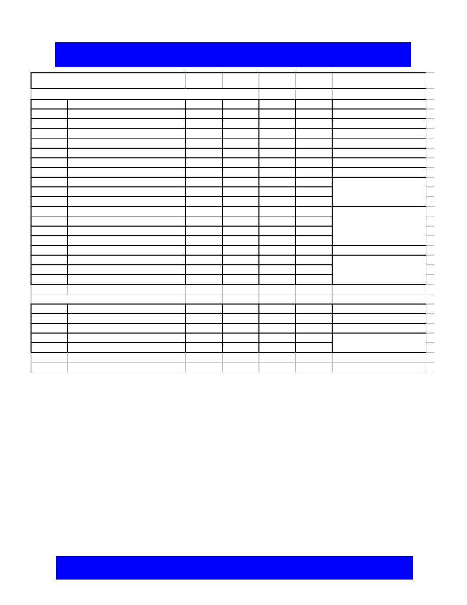
Electrical Characteristics @T
J
25∫C (Unless otherwise specified)
Symbol
Parameter
Min.
Typ.
Max.
Units
Test Conditions
BVDSS
Drain to Source Breakdown Voltage
60
V
V
GS
=0V, I
D
=1.0mA
Rds(on)
Static Drain to Source On Resistance
4
5
m Ohms
V
GS
=10V,I
D
=76Amps
ID(on)
On-State Drain Current
150
A
V
DS
>I
D(on)x
RD
S(on)
max V
GS
=10V
V
GS (th)
Gate threshold Voltage
2
4
V
V
DS
=V
GS
I
D
=1.0mA
Gfs
Forward Transconductance
124
188
S
V
DS
>50V I
D
=150A
I
DSS
Zero Gate Voltage Drain Current
1
mA
V
DS
=V
DS
max V
GS
=0V
I
GSS
Gate to Source Leakage
±400
nA
V
GS
=20V
Qg
Total Gate Charge
520
600
nC
Qgs
Gate to Source Charge
100
148
nC
Qgd
Gate to drain Charge
180
272
nC
t
d(on)
Turn on Delay
110
ns
t
r
Rise Time
700
ns
t
d(off)
Turn off Delay Time
400
ns
t
f
Fall Time
260
ns
L
DS
Drain to Source Inductance
18
nH
C
iss
Input Capacitance
9.3
nF
C
oss
Output Capacitance
1.7
nF
C
rss
Reverse Transfer Capacitance
0.5
nF
Source-Drain Diode Ratings and Characteristics
I
S
Continuous Source Current
150
A
I
SM
Pulse Source Current
800
A
V
SD
Diode Forward Votage
2.5
V
V
GS
=0V I
S
=150A
t
rr
Reverse Recovery Time
71
150
320
ns
Qrr
Reverse Recovery Charge
4.4
10
23
µC
V
DD
=25V I
D
=150A V
GS
=10V
R
source
=3.3 OHMs
V
GS
=0V,V
DS
=25, f=1MHz
di/dt=400A/µs I
S
=150A
I
D
=150A V
GS
=10V V
DS
=V
DSmaxX
0.80
