
752B\X]X
8B3=!13B
8B3=73;2585>R^]ca^[[Ta
fXcW
BCX]cTaUPRT
P]S
X]cTVaPcTS585>b
0dVdbc!
Copyright 1994-2001 Cologne Chip AG
All Rights Reserved
The information presented can not be considered as assured characteristics. Data can change without notice. Parts of the
information presented may be protected by patent or other rights. Cologne Chip products are not designed, intended, or
authorized for use in any application intended to support or sustain life, or for any other application in which the failure of
the Cologne Chip product could create a situation where personal injury or death may occur.
"3@3
+:77@
Cologne
Chip
863C ]Y^Y
" _V '(
1eWecd " !
Cologne
Chip
Revision History
Date
Remarks
Aug. 2001
Chapters added: Timing diagrams for Motorala mode (mode2), Sample circuitries.
Jul. 2001
Information added to: Register description.
Jan. 2001
Information added to: Microprocessor access, PCM/GCI/IOM2 timing.
Nov. 2000
preliminary edition.
Cologne
Chip
Cologne Chip AG
Eintrachtstrasse 113
D-50668 K�ln
Germany
Tel.: +49 (0) 221 / 91 24-0
Fax: +49 (0) 221 / 91 24-100
http://www.CologneChip.com
http://www.CologneChip.de
info@CologneChip.com

863C ]Y^Y
1eWecd " !
# _V '(
Cologne
Chip
Contents
Features........................................................................................................................................................ 6
1
General description............................................................................................................................ 6
1.1
Block diagram.................................................................................................................................. 7
1.2
Applications ..................................................................................................................................... 7
1.3
Processor interface modes ............................................................................................................... 8
2
Pin description.................................................................................................................................... 9
2.1
S/T interface transmit signals .......................................................................................................... 9
2.2
S/T interface receive signals............................................................................................................ 9
2.3
PCM bus interface signals ............................................................................................................. 10
2.4
Processor interface signals............................................................................................................. 10
2.5
Miscellaneous pins......................................................................................................................... 11
2.6
Oscillator........................................................................................................................................ 11
2.7
Power supply.................................................................................................................................. 11
3
Functional description ..................................................................................................................... 12
3.1
Microprocessor interface ............................................................................................................... 12
3.1.1
Register access ...................................................................................................................... 12
3.2
FIFOs ............................................................................................................................................. 13
3.2.1
FIFO channel operation......................................................................................................... 14
3.2.1.1
Send channels (B1, B2, D and PCM transmit) ................................................................. 15
3.2.1.2
Automatically D-channel frame repetition ....................................................................... 15
3.2.1.3
FIFO full condition in send channels................................................................................ 16
3.2.1.4
Receive Channels (B1, B2, D and PCM receive) ............................................................. 16
3.2.1.5
FIFO full condition in receive channels ........................................................................... 17
3.2.2
FIFO initialization................................................................................................................. 18
3.2.3
FIFO reset.............................................................................................................................. 18
3.3
Transparent mode of HFC-S mini.................................................................................................. 19
3.4
Correspondency between FIFOs, CHANNELs and SLOTs .......................................................... 20
3.5
Subchannel Processing .................................................................................................................. 25
3.6
PCM Interface Function................................................................................................................. 26
3.7
Configuring test loops.................................................................................................................... 28
4
Register description ......................................................................................................................... 29
4.1
Register reference list .................................................................................................................... 29
4.1.1
Registers by address.............................................................................................................. 29
4.1.2
Registers by name ................................................................................................................. 30
4.2
FIFO, interrupt, status and control registers .................................................................................. 31
4.3
PCM/GCI/IOM2 bus section registers........................................................................................... 39
4.4
S/T section registers....................................................................................................................... 43
5
Electrical characteristics ................................................................................................................. 47
6
Timing characteristics ..................................................................................................................... 50
6.1
Microprocessor access ................................................................................................................... 50
6.1.1
Register read access in de-multiplexed Motorola mode (mode 2)........................................ 50
6.1.2
Register write access in de-multiplexed Motorola mode (mode 2) ...................................... 51
6.1.3
Register read access in de-multiplexed Intel mode (mode 3) ............................................... 52
6.1.4
Register write access in de-multiplexed Intel mode (mode 3) .............................................. 53

863C ]Y^Y
$ _V '(
1eWecd " !
Cologne
Chip
6.1.5
Register read access in multiplexed mode (mode 4)............................................................. 54
6.1.6
Register write access in multiplexed mode (mode 4) ........................................................... 55
6.2
PCM/GCI/IOM2 timing................................................................................................................. 56
6.2.1
Master mode.......................................................................................................................... 57
6.2.2
Slave mode ............................................................................................................................ 58
7
External circuitries........................................................................................................................... 59
7.1
S/T interface circuitry .................................................................................................................... 59
7.1.1
External receiver circuitry..................................................................................................... 59
7.1.2
External wake-up circuitry.................................................................................................... 60
7.1.3
External transmitter circuitry ................................................................................................ 61
7.2
Oscillator circuitry for S/T clock................................................................................................... 64
8
State matrices for NT and TE ......................................................................................................... 65
8.1
S/T interface activation/deactivation layer 1 for finite state matrix for NT .................................. 65
8.2
Activation/deactivation layer 1 for finite state matrix for TE ....................................................... 66
9
Binary organisation of the frames .................................................................................................. 67
9.1
S/T frame structure ........................................................................................................................ 67
9.2
GCI frame structure ....................................................................................................................... 68
10
Clock synchronisation...................................................................................................................... 69
10.1
Clock synchronisation in NT-mode........................................................................................... 69
10.2
Clock synchronisation in TE-mode ........................................................................................... 70
10.3
Multiple HFC-S mini SYNC scheme ........................................................................................ 71
11
HFC-S mini package dimensions.................................................................................................... 72
12
Sample circuitries............................................................................................................................. 73
12.1
HFC-S mini in mode 2 (Motorola bus) ..................................................................................... 73
12.2
HFC-S mini in mode 3 (Intel bus with separated address bus/data bus)................................... 75
12.3
HFC-S mini in mode 4 (Intel bus with multiplexed address bus/data bus)............................... 77

863C ]Y^Y
1eWecd " !
% _V '(
Cologne
Chip
Figures
Figure 1: HFC-S mini block diagram............................................................................................................ 7
Figure 2: Pin Connection .............................................................................................................................. 9
Figure 3: FIFO Organisation....................................................................................................................... 14
Figure 4: FIFO Data Organisation .............................................................................................................. 16
Figure 5: FIFOs, CHANNELs and SLOTs in Transmit Direction ............................................................. 22
Figure 6: FIFOs, CHANNELs and SLOTs in Receive Direction............................................................... 23
Figure 7: Example for Subchannel Processing ........................................................................................... 25
Figure 8: PCM Interface Function Block Diagram..................................................................................... 26
Figure 9: Function of CON_HDLC register bits 7..5 ................................................................................. 37
Figure 10: External receiver circuitry......................................................................................................... 59
Figure 11: External wake-up circuitry ........................................................................................................ 60
Figure 12: External transmitter circuitry .................................................................................................... 61
Figure 13: Oscillator circuitry for S/T clock .............................................................................................. 64
Figure 14: Frame structure at reference point S and T ............................................................................... 67
Figure 15: Single channel GCI format........................................................................................................ 68
Figure 16: Clock synchronisation in NT-mode .......................................................................................... 69
Figure 17: Clock synchronisation in TE-mode ........................................................................................... 70
Figure 18: Multiple HFC-S mini SYNC scheme ........................................................................................ 71
Figure 19: HFC-S mini package dimensions .............................................................................................. 72
Tables
Table 1: Function of the microprocessor interface control signals ............................................................ 12
Table 2: Possible connections of FIFOs and CHANNELs in Simple Mode (SM)..................................... 20
Table 3: CHANNEL Numbers on the S/T Interface and PCM Interface ................................................... 21
Table 4: S/T module part numbers and manufacturers............................................................................... 63
Table 5: Activation/deactivation layer 1 for finite state matrix for NT ..................................................... 65
Table 6: Activation/deactivation layer 1 for finite state matrix for TE ...................................................... 66
Timing diagrams
Timing diagram 1: Register read access in de-multiplexed Motorola mode (mode 2) .............................. 50
Timing diagram 2: Register write access in de-multiplexed Motorola mode (mode 2) ............................. 51
Timing diagram 3: Register read access in de-multiplexed Intel mode (mode 3) ...................................... 52
Timing diagram 4: Register write access in de-multiplexed Intel mode (mode 3)..................................... 53
Timing diagram 5: Register read access in multiplexed mode (mode 4) ................................................... 54
Timing diagram 6: Register write access in multiplexed mode (mode 4) .................................................. 55
Timing diagram 7: PCM/GCI/IOM2 timing ............................................................................................... 56

863C ]Y^Y
& _V '(
1eWecd " !
Cologne
Chip
Features
single chip ISDN-S/T-controller with B- and D-channel HDLC support
integrated S/T interface
full I.430 ITU S/T ISDN support in TE and NT mode for 3.3V and 5V power supply
independent read and write HDLC-channels for 2 ISDN B-channels, one ISDN D-channel and
one PCM timeslot (or E-channel)
B1- and B2-channel transparent mode independently selectable
integrated FIFOs for B1, B2, D and PCM (or E)
FIFO size: 128 bytes per channel and direction; up to 7 HDLC frames per FIFO
56 kbit/s restricted mode for U.S. ISDN lines selectable by software
PCM128 / PCM64 / PCM30 interface configurable to interface MITEL ST
TM
bus (MVIP
TM
),
Siemens IOM2
TM
or GCI
TM
for interface to U-chip or external CODECs
H.100 data rate supported
microprocessor interface compatible to Motorola bus and Intel bus
Timer with interrupt capability
CMOS technology, 3V - 5V
PQFP 48 case
1
General description
The HFC-S mini is a single-chip ISDN S/T HDLC basic rate controller for embedded applications.
The S/T interface, HDLC-controllers, FIFOs and a microprocessor interface are integrated in the HFC-S
mini. A PCM128 / PCM64 / PCM30 interface is also implemented which can be connected to many
telecom serial busses. CODECs are usually connected to this interface. All ISDN channels (2B+1D) and
the PCM interface are served fully duplex by the 8 integrated FIFOs.
HDLC controllers are implemented in hardware so there is no need to implement HDLC on the host
processor.

863C ]Y^Y
1eWecd " !
' _V '(
Cologne
Chip
1.1
Block diagram
S/T-
controller
4x HDLC B-channel
2x HDLC D-channel
2x HDLC
microprocessor interface
FIFOs
U-chip
PCM128
PCM64
PCM30
MST
IOM2
GCI
CODEC
select
S/
T
U
HFC
-
S
mini
TM
microprocessor
D-transmit
D-receive
B1-transmit
B1-receive
B2-transmit
B2-receive
PCM-trans.
PCM-rec.
PCM128/
PCM64/
PCM30
interface
Figure 1: HFC-S mini block diagram
1.2
Applications
The HFC-S mini can be used for all kinds of ISDN equipment with ISDN basic rate S/T interface.
ISDN terminal adapters (for Internet access)
ISDN terminal adapters (with POTS interfaces)
ISDN
PABX
ISDN SoHo PABX (switching done by HFC-S mini)
ISDN
telephones
ISDN video conferencing equipment
ISDN dialers / LCR (Least Cost Routers)
ISDN LAN Routers
ISDN protocol analyzers
ISDN smart NTs

863C ]Y^Y
( _V '(
1eWecd " !
Cologne
Chip
1.3
Processor interface modes
The HFC-S mini has an integrated 8-bit microprocessor interface which can be configured into Motorola
bus, de-multiplexed Intel bus and multiplexed Intel bus. The different interface modes are selected during
power on by ALE.
Mode 2:
Motorola bus with control signals /CS, R/W, /DS is selected by setting ALE to VDD.
Mode 3:
Intel bus with seperated address bus (A0) and data bus (D[7:0]) and control signals /CS,
/WR, /RD is selected by setting ALE to GND.
Mode 4:
Intel bus with multiplexed address bus and data bus with control signals /CS, /WR, /RD,
ALE. ALE must be '0' during power on to select this mode. A0 must be '0'.
ALE latches the address. The multiplexed address/data bus is D[7:0].
In mode 4 all internal registers can be directly accessed. In mode 2 and mode 3 first the address of the
desired register must be written to the address with A0 = '1'. Afterwards data can be read/written from/to
that register by reading/writing the address with A0 = '0'.
In mode 4 A0 must be '0'.

863C ]Y^Y
1eWecd " !
) _V '(
Cologne
Chip
2
Pin description
Figure 2: Pin Connection
2.1
S/T interface transmit signals
Pin No.
Pin Name
Input
Output
Function
13
TX2_HI
O
Transmit output 2
14
/TX1_LO
O
GND driver for transmitter 1
15
/TX_EN
O
Transmit enable
16
/TX2_LO
O
GND driver for transmitter 2
17
TX1_HI
O
Transmit output 1
2.2
S/T interface receive signals
20
R2
I
Receive data 2
21
LEV_R2
I
Level detect for R2
22
LEV_R1
I
Level detect for R1
23
R1
I
Receive data 1
25
ADJ_LEV
O
Level generator
28
AWAKE
I
Awake input pin for external awake circuitry

863C ]Y^Y
! _V '(
1eWecd " !
Cologne
Chip
2.3
PCM bus interface signals
30
C4IO
I/O
u)
4.096 MHz / 8.192 MHz / 16.384 MHz clock
PCM/GCI/IOM2 bus clock master: output
PCM/GCI/IOM2 bus clock slave: input (reset default)
31
F0IO
I/O
u)
Frame synchronisation, 8kHz pulse for PCM/GCI/IOM2 bus
frame synchronisation
PCM/GCI/IOM2 bus master: output
PCM/GCI/IOM2 bus slave: input (reset default)
32
STIO1
I/O
u)
PCM/GCI/IOM2 bus data line I
Slotwise programmable as input or output
33
STIO2
I/O
u)
PCM/GCI/IOM2 bus data line II
Slotwise programmable as input or output
34
F1_A
O
enable signal for external CODEC A or C2IO clock (bit clock)
Programmable as positive (reset default) or negative pulse.
35
F1_B
O
enable signal for external CODEC B
Programmable as positive (reset default) or negative pulse.
u)
internal pull up
2.4
Processor interface signals
Pin No.
Pin Name
Input
Output
Mode Function
4
D0
I/O
all
Data bus (bit 0)
5
D1
I/O
all
Data bus (bit 1)
6
D2
I/O
all
Data bus (bit 2)
7
D3
I/O
all
Data bus (bit 3)
8
D4
I/O
all
Data bus (bit 4)
9
D5
I/O
all
Data bus (bit 5)
10
D6
I/O
all
Data bus (bit 6)
11
D7
I/O
all
Data bus (bit 7)
47
A0
I
2, 3
Address bit 0 from external processor
2
/WR
R/W
I
I
3, 4
2
Write signal from external processor (low active)
Read/Write select (WR='0')
1
/RD
/DS
I
I
3, 4
2
Read signal from external processor (low active)
I/O data strobe
46
/CS
I
u)
all
Chip select (low active)
45
ALE
I
u)
Address latch enable
ALE is also used for mode selection during power on
(see also 1.3 Processor interface mode on page 8).
36
/WAIT
O
e)
all
Wait signal for external processor (low active)
u)
internal pull up
e)
external pull up required

863C ]Y^Y
1eWecd " !
!! _V '(
Cologne
Chip
2.5
Miscellaneous pins
Pin No.
Pin Name
Input
Output
Function
38
SYNC_I
I
8 kHz sync input
43
SYNC_O
O
8 kHz sync output
42
NC
Not connected (pin must be left open)
44
/INT
O
Interrupt request for external processor (low active)
48
/RES
I
u)
Reset (low active)
u)
internal pull up
2.6
Oscillator
Pin No.
Pin Name
Input
Output
Function
26
CLKI
I
24.576 MHz clock input or 24.576 MHz crystal
27
CLKO
O
24.576 MHz clock output or 24.576 MHz crystal
2.7
Power supply
Pin No.
Pin Name
Function
3, 19, 40
VDD
VDD (3.3V or 5V)
12, 18, 24, 29, 37, 39, 41
GND
GND

863C ]Y^Y
!" _V '(
1eWecd " !
Cologne
Chip
3
Functional description
3.1
Microprocessor interface
The HFC-S mini has an integrated 8 bit microprocessor interface. It is compatibel with Motorola bus and
Intel bus. The different microprocessor interface modes are selected during power on by ALE (see also
1.3 Processor interface modes on page 8).
In mode 2 (Motorola bus mode) and mode 3 (de-multiplexed Intel bus mode) pin A0 is the address input.
The data bus is D[7:0].
In mode 4 (multiplexed Intel bus mode) D[7:0] is the multiplexed address/data bus. A0 must be '0' in this
mode.
3.1.1
Register access
In mode 2 and mode 3 the HFC-S mini has 2 addresses. The lower address (A0 = '0') is used for data
read/write. The higher address (A0 = '1') is write only and is used for register selection. Registers are
selected by first setting A0 to '1' and then writing the address of the desired register to the data bus
D[7:0]. All following accesses to the HFC-S mini with A0 = '0' are read/write operations to this register.
In mode 4 all registers can be directly accessed by their address.
The function of the control signals is shown in the table below.
/RD
/DS
/WR
R/W
/CS
ALE
Operation
Mode
X
X
1
X
no access
all
1
1
X
X
no access
all
0
1
0
1
read data
2
0
0
0
1
write data
2
0
1
0
0
read data
3
1
0
0
0
write data
3
0
1
0
0
*)
read data
4
1
0
0
0
*)
write data
4
Table 1: Function of the microprocessor interface control signals
X = don't care
*)
1-pulse latches register address.
Except in mode 4 ALE is assumed to be stable after RESET.

863C ]Y^Y
1eWecd " !
!# _V '(
Cologne
Chip
3.2
FIFOs
There is a transmit and a receive FIFO with HDLC-controller for each of the two B-channels, for the D-
channel and for the PCM interface in the HFC-S mini. Each FIFO has 128 bytes length in each direction.
Up to 7 frames can be stored in each FIFO.
The HDLC circuits are located on the S/T device side of the HFC-S mini. So always plain data is stored
in the FIFOs. Zero insertion and CRC checksum processing for receive and transmit data is done by the
HFC-S mini automatically.
A FIFO can be selected for access by writing its number in the FIFO select register (FIFO#).
The FIFOs are ring buffers. To control them there are some counters. Z1 is the FIFO input counter and
Z2 is the FIFO output counter.
Each counter points to a byte position in the SRAM. On a FIFO input operation Z1 is incremented. On an
output operation Z2 is incremented.
After every pulse on the F0IO signal two HDLC-bytes are written into the S/T interface (FIFOs with
even numbers) and two HDLC-bytes are read from the S/T interface (FIFOs with odd numbers).
D-channel data is handled in a similar way but only 2 bits are processed.
*
important!
Instead of the S/T interface also PCM bus is selectable for each B-channel (see CON_HDLC
register).
If Z1 = Z2 the FIFO is empty.
Additionally there are two counters F1 and F2 for every FIFO channel (3 bits for each channel). They
count the HDLC-frames in the FIFOs and form a ring buffer as Z1 and Z2 do, too.
F1 is incremented when a complete frame has been received and stored in the FIFO. F2 is incremented
when a complete frame has been read from the FIFO.
If F1 = F2 there is no complete frame in the FIFO.
When the RESET line is active or software reset is active Z1, Z2, F1 and F2 are all initialized to all 1s
(so Z-counters are initialized to 7Fh and F-counters are initialized to 07h).
The access to a FIFO is selected by writing the FIFO number into the FIFO select register (FIFO#).

863C ]Y^Y
!$ _V '(
1eWecd " !
Cologne
Chip
*
important!
FIFO change, FIFO reset and F1/F2 incrementation
Changing the FIFO, reseting the FIFO or incrementing the frame counters causes a short BUSY
period of the HFC-S mini. This means an access to FIFO control registers is NOT allowed until
BUSY status is reset (bit 0 of STATUS register). This has a maximum duration of 25 clock cycles
(2�s). Status, interrupt and control registers can be read and written at any time.
*
important!
The counter state 00h of the Z-counters follows counter state 7Fh in the B-, D- and PCM FIFOs.
The counter state 00h of the F-counters follows counter state 07h in the B-, D- and PCM FIFOs.
3.2.1
FIFO channel operation
Figure 3: FIFO Organisation

863C ]Y^Y
1eWecd " !
!% _V '(
Cologne
Chip
3.2.1.1
Send channels (B1, B2, D and PCM transmit)
The send channels send data from the host bus interface to the FIFO and the HFC-S mini converts the
data into HDLC code and tranfers it from the FIFO into the S/T or/and the PCM bus interface write
registers.
The HFC-S mini checks Z1 and Z2. If Z1=Z2 (FIFO empty) the HFC-S mini generates a HDLC-Flag
(01111110) or idle pattern (1111 1111) and sends it to the S/T device. In this case Z2 is not incremented.
If also F1=F2 only HDLC flags are sent to the S/T interface and all counters remain unchanged. If the
frame counters are unequal F2 is incremented and the HFC-S mini tries to send the next frame to the
output device. After the end of a frame (Z2 reaches Z1) it automatically generates the 16 bit CRC
checksum and adds the ending flag. If there is another frame in the FIFO (F1
F2) the F2 counter is
incremented.
With every byte being sent from the host bus side to the FIFO Z1 is incremented automatically. If a
complete frame has been sent F1 must be incremented to send the next frame. If the frame counter F1 is
incremented also the Z-counters may change because Z1 and Z2 are functions of F1 and F2. So there are
Z1(F1), Z2(F1), Z1(F2) and Z2(F2) (see Figure 3).
Z1(F1) is used for the frame which is just written from the microprocessor bus side. Z2(F2) is used for
the frame which is just beeing transmitted to the S/T device side of the HFC-S mini. Z1(F2) is the end of
frame pointer of the current output frame.
In the send channels F1 is only changed from the microprocessor interface side if the software driver
wants to say ,,end of send frame". Then the current value of Z1 is stored, F1 is incremented and Z1 is
used as start address of the next frame. Z1(F2) and Z2(F2) can not be accessed.
* important!
The HFC-S mini begins to transmit the bytes from a FIFO at the moment the FIFO is changed or
the F1 counter is incremented. Also changing to the FIFO that is already selected starts the
transmission. So by selecting the same FIFO again transmission can be started. This is required if a
HDLC frame is longer than 128 bytes.
3.2.1.2
Automatically D-channel frame repetition
The D-channel send FIFO has a special feature. If the S/T interface signals a D-channel contention
before the CRC is sent the Z2 counter is set to the starting address of the current frame and the HFC-S
mini tries to repeat the frame automatically.

863C ]Y^Y
!& _V '(
1eWecd " !
Cologne
Chip
3.2.1.3
FIFO full condition in send channels
There are two different FIFO full conditions. The first one is met when the FIFO contents comes up to 7
frames. There is no possibility for the HFC-S mini to manage more frames even if the frames are very
small. The driver software must check that there are never more than 7 HDLC frames in a FIFO.
The second limitation is the size of the FIFO (128 bytes each). FIFO full condition can be checked by
reading the F_USAGE register. It shows the actually occupied FIFO space in bytes.
Furthermore a threshold value can be set for all transmit and receive FIFOs in the F_THRES register.
Then the F_FILL register shows an indication for the filling level for each FIFO.
3.2.1.4
Receive Channels (B1, B2, D and PCM receive)
The receive channels receive data from the S/T or PCM bus interface read registers. The data is
converted from HDLC into plain data and sent to the FIFO. The data can then be read via the
microprocessor bus interface.
The HFC-S mini checks the HDLC data coming in. If it finds a flag or more than 5 consecutive 1s it does
not generate any output data. In this case Z1 is not incremented. Proper HDLC data being received is
converted by the HFC-S mini into plain data. After the ending flag of a frame the HFC-S mini checks the
HDLC CRC checksum. If it is correct one byte with all 0s is inserted behind the CRC data in the FIFO
named STAT. This last byte of a frame in the FIFO is different from all 0s if there is no correct CRC
field at the end of the frame.
Figure 4: FIFO Data Organisation

863C ]Y^Y
1eWecd " !
!' _V '(
Cologne
Chip
The ending flag of a HDLC-frame can also be the starting flag of the next frame.
After a frame is received completely F1 is incremented by the HFC-S mini automatically and the next
frame can be received.
After reading a frame via the microprocessor bus interface F2 must be incremented. If the frame counter
F2 is incremented also the Z-counters may change because Z1 and Z2 are functions of F1 and F2. So
there are Z1(F1), Z2(F1), Z1(F2) and Z2(F2) (see Figure 3).
Z1(F1) is used for the frame which is just received from the S/T device side of the HFC-S mini. Z2(F2) is
used for the frame which is just beeing transmitted to the microprocessor bus interface. Z1(F2) is the end
of frame pointer of the current output frame.
To calculate the length of the current receive frame the software has to evaluate Z1-Z2+1. When Z2
reaches Z1 the complete frame has been read.
In the receive channels F2 must be incremented from the microprocessor bus interface side after the
software detects an end of receive frame (Z1=Z2) and F1
F2. Then the current value of Z2 is stored, F2
is incremented and Z2 is copied as start address of the next frame. If Z1 = Z2 and F1 = F2 the FIFO is
totally empty. Z1(F1) can not be accessed.
* important!
Before reading a FIFO a change FIFO operation (see also: FIFO# register) must be done even if
the desired FIFO is already selected. The change FIFO operation is required to update the internal
buffer of the HFC-S mini. Otherwise the first byte of the FIFO will be taken from the internal
buffer and may be invalid.
3.2.1.5
FIFO full condition in receive channels
Because the ISDN-B-channels and the ISDN-D-channels have no hardware based flow control there is no
possibility to stop input data if a receive FIFO is full.
So there is no FIFO full condition implemented in the HFC-S mini. The HFC-S mini assumes that the
FIFOs are so deep that the host processors hard- and software is able to avoid any overflow of the receive
FIFOs. Overflow conditions are again more than 7 input frames or a real overflow of the FIFO because
of excessive data (more than 128 bytes).
Because HDLC procedures only know a window size of 7 frames no more than 7 frames are sent without
software intervention.
The register F_FILL indicates if the fill level of some FIFOs exceeds the number of bytes defined in the
F_THRES register. A byte overflow can be avoided by polling this register.
However to avoid any undetected FIFO overflows the software driver should check the number of frames
in the FIFO which is F1-F2. An overflow exists if the number (F1-F2) is less than the number in the last
reading even if there was no reading of a frame in between.
After a detected FIFO overflow condition this FIFO must be reset by setting the FIFO reset bit in the
INC_RES_F register.

863C ]Y^Y
!( _V '(
1eWecd " !
Cologne
Chip
3.2.2
FIFO initialization
After reset all FIFOs are disabled. To enable a FIFO at least one of bits[4:1] of the CON_HDLC register
for the corresponding FIFO must be set to '1'.
For D-channel FIFOs the inter frame fill bit (bit 0 of CON_HDLC register) must be set to '1'. The
HDLC_PAR register must be set to 02h ('0000 0010').
3.2.3
FIFO reset
All counters Z1, Z2, F1 and F2 of all FIFOs are initialized to all 1s after a RESET.
Then the result is Z1 = Z2 = 7Fh and F1 = F2 = 07h.
The same initialisation is done if the bit 3 in the CIRM register is set (soft reset).
Single FIFOs can be reset by setting bit 1 of INC_RES_F register.

863C ]Y^Y
1eWecd " !
!) _V '(
Cologne
Chip
3.3
Transparent mode of HFC-S mini
You can switch off HDLC operation for each B-channel independently. There is one bit for each B-
channel in the CON_HDLC control register. If this bit is set data in the FIFO is sent directly to the S/T or
PCM bus interface and data from the S/T or PCM bus interface is sent directly to the FIFO.
The FIFOs should be empty when switching into transparent mode.
If a send FIFO channel changes to FIFO empty condition no CRC is generated and the last data byte in
the FIFO memory is repeated until there is new data. If the last data byte which was written to the
selected FIFO should be repeated the last byte must be written without increment of Z-counter
(FIF_DATA register, address 84h).
In receive channels there is no check on flags or correct CRCs and no status byte is added.
The byte bounderies are not arbitrary like in HDLC mode where byte synchronisation is achieved with
HDLC-flags. The data is just the same as it comes from the S/T or PCM bus interface or is sent to this.
Send and receive transparent data can be handled in two ways. The usual way is transporting B-channel
data with the LSB first as it is usual in HDLC mode. The second way is sending the bytes in reverse bit
order as it is usual for PWM data. So the first bit is the MSB. The bit order can be reversed by setting the
corresponding bit in the F_CROSS register.

863C ]Y^Y
" _V '(
1eWecd " !
Cologne
Chip
3.4
Correspondency between FIFOs, CHANNELs and SLOTs
For the data processing of the HFC-S mini you must distinguish between FIFOs, CHANNELs and
SLOTs.
The FIFOs are buffers between the microprocessor interface and the data interfaces PCM and/or S/T.
The HDLC controllers are located on the non host bus side of the FIFOs.
The CHANNELs are either mapped to the data channels on the S/T interface (then the CHANNEL
selects the S/T channel as shown in Table 3) or they can be connected to arbitrary timeslots on the PCM
interface. SLOTs are 8 bit timeslots on the PCM interface.
The following values (registers) characterise FIFOs, CHANNELs and SLOTs:
FIFO:
FIFO#
CHANNEL: CHANNEL#
SLOT:
B1_RSL, B1_SSL, B2_RSL, B2_SSL, AUX1_RSL, AUX1_SSL, AUX2_RSL and
AUX2_SSL
Even numbers (LSB = '0') always belong to a transmit FIFO, transmit CHANNEL (see also: Table 3).
Odd numbers (LSB = '1') always belong to a receive FIFO, receive CHANNEL (see also: Table 3).
In Simple Mode (F_MODE register bit 7 = '0', SM) the CHANNEL number equals the FIFO number. But
it is possible to connect each FIFO to a PCM timeslot instead of the S/T interface in this mode (see table
below).
FIFO-No.
(FIFO#, bits 2..0)
CHANNEL after RESET Possible Connections in Simple Mode (SM)
(CON_HDLC, bits 7..5)
'000'
B1-transmit channel (S/T)
B1-transmit channel (S/T)
PCM-transmit timeslot selected by B1_SSL
'001'
B1-receive channel (S/T)
B1-receive channel (S/T)
PCM-receive timeslot selected by B1_RSL
'010'
B2-transmit channel (S/T)
B2-transmit channel (S/T)
PCM-transmit timeslot selected by B2_SSL
'011'
B2-receive channel (S/T)
B1-receive channel (S/T)
PCM-receive timeslot selected by B2_RSL
'100'
D-transmit channel (S/T)
D-transmit channel (S/T)
PCM-transmit timeslot selected by AUX1_SSL
'101'
D-receive channel (S/T)
D-receive channel (S/T)
PCM-receive timeslot selected by AUX1_RSL
'110'
invalid (E is receive only)
PCM-transmit timeslot selected by AUX2_SSL
'111'
E-receive channel (S/T)
E-receive channel (S/T)
PCM-receive timeslot selected by AUX2_RSL
Table 2: Possible connections of FIFOs and CHANNELs in Simple Mode (SM)

863C ]Y^Y
1eWecd " !
"! _V '(
Cologne
Chip
In Channel Select Mode (F_MODE register bit 7 = '1', CSM) FIFOs can be associated with arbitrary
CHANNELs.
FIFOs are selected by writing their number in the FIFO# register. All FIFOs are disabled after
initialization (reset). By setting at least one of the CON_HDLC register bits 3..1 to '1' the selected FIFO
is enabled.
The connection between a FIFO and a CHANNEL can be established by the CHANNEL# register for
each FIFO if Channel Select Mode is enabled (F_MODE register bit 7 = '1', CSM). Otherwise the
CHANNEL number equals the FIFO number.
The channels on the S/T interface (B1, B2, D and E) and PCM interface (B1, B2, AUX1 and AUX2) are
numbered as follows:
CHANNEL Number
(CHANNEL#, bits 2..0)
ISDN Channel on the
S/T Interface
ISDN Channel on the
PCM Interface
'000'
'001'
'010'
'011'
'100'
'101'
'110'
'111'
B1-transmit
B1-receive
B2-transmit
B2-receive
D-transmit
D-receive
invalid (E is receive only)
E-receive
B1-transmit
B1-receive
B2-transmit
B2-receive
AUX1-transmit
AUX1-receive
AUX2-transmit
AUX2-receive
Table 3: CHANNEL Numbers on the S/T Interface and PCM Interface
The data flow between the HFC part (FIFOs), S/T interface and PCM interface can be selected by the
CON_HDLC register (bits 7..5) for each FIFO.
The PCM timeslot for B1, B2, AUX1 and AUX2 can be specified by the timeslot assigner (registers
B1_RSL, B1_SSL, B2_RSL, B2_SSL, AUX1_RSL, AUX1_SSL, AUX2_RSL and AUX2_SSL).
Data of a CHANNEL can furthermore be looped over the PCM interface (and the timeslot assigner).

863C ]Y^Y
"" _V '(
1eWecd " !
Cologne
Chip
CHANNEL
SLOT
FIFO
Number
CHANNEL
Number
Sub-
Channel
Processing
HDLC
Data
Transparent
Data
PCM
S/T
[T1]
Transmit Channel
for FIFO
[T2]
Bit Count / Start Bit /
Mask Bits
for Transmit Channel
[T3]
Select Data
Flow for
Transmit Channel
[T4]
Select PCM Slot No.
for Transmit Channel
see also: PCM Interface Function
FIFOs
CONNECT
MEMORY
Figure 5: FIFOs, CHANNELs and SLOTs in Transmit Direction
[T1]
In Simple Mode (SM) the CHANNEL number is the same as the FIFO number. If Channel Select
Mode (CSM) is enabled the transmit CHANNEL for a FIFO can be selected by
1)
writing the FIFO number (0..7) in the FIFO# register
2)
writing the desired CHANNEL number (0..7) to the CHANNEL# register (bits 2..0)
Please note that transmit CHANNELs are even numbered (bit 0 of CHANNEL# register = '0').
[T2]
The bit values for the not processed bits of the transmit CHANNEL are read from the
CH_MASK register. The processed bits are taken from the FIFO (see also: Subchannel
Processing). Please note that more than one FIFO can transmit data to the same CHANNEL. This
is useful to combine subchannels and transmit them in one ISDN channel.
[T3]
Data can either be transmitted to the S/T interface or the PCM interface.
1)
write the FIFO number (0..7) in the FIFO# register
2)
write the desired connection to the CON_HDLC register bits 7..5
The CON_HDLC register bits 7..5 settings must be the same for corresponding receive and
transmit FIFOs.

863C ]Y^Y
1eWecd " !
"# _V '(
Cologne
Chip
[T4]
A PCM SLOT can be connected to a CHANNEL.
FIFO-No.
(FIFO#, bits 2..0)
Register for
Timeslot
Selection
'000'
B1_SSL
'001'
B1_RSL
'010'
B2_SSL
'011'
B2_RSL
'100'
AUX1_SSL
'101'
AUX1_RSL
'110'
AUX2_SSL
'111'
AUX2_RSL
The PCM SLOT number for a FIFO can be selected by writing the desired SLOT number to its
timeslot selection register shown in the table above. Please note that only the *_SSL registers are
for transmit slots.
CHANNEL
SLOT
FIFO
Number
CHANNEL
Number
Sub-
Channel
Processing
HDLC
Data
Transparent
Data
PCM
S/T
[R1]
Receive Channel
for FIFO
[R2]
Bit Count / Start Bit /
Mask Bits
for Receive Channel
[R3]
Select Data
Flow for
Receive Channel
[R4]
Select PCM Slot No.
for Receive Channel
see also: PCM Interface Function
FIFOs
CONNECT
MEMORY
Figure 6: FIFOs, CHANNELs and SLOTs in Receive Direction

863C ]Y^Y
"$ _V '(
1eWecd " !
Cologne
Chip
[R1]
In Simple Mode (SM) the CHANNEL number is the same as the FIFO number. If Channel Select
Mode (CSM) is enabled the transmit CHANNEL for a FIFO can be selected by
1)
writing the FIFO number (0..7) in the FIFO# register
2)
writing the desired CHANNEL number (0..7) to the CHANNEL# register (bits 2..0)
Please note that receive CHANNELs are odd numbered (bit 0 of CHANNEL# register = '1').
[R2]
The bit values of the not processed bits of the receive CHANNEL are ignored. The processed
bits are taken from the CHANNEL (see also: Subchannel Processing). Please note that more than
one FIFO can receive data from the same CHANNEL (e.g. bits 1..0 are processed by FIFO 1 and
bits 3..2 by FIFO 3). This is useful to split subchannels that have been combined to be
transmitted in one ISDN channel.
[R3]
Data can either be received from the S/T interface or the PCM interface.
1)
write the FIFO number (0..7) in the FIFO# register
2)
write the desired connection to the CON_HDLC register bits 7..5
The CON_HDLC register bits 7..5 settings must be the same for corresponding receive and
transmit FIFOs.
[R4]
A PCM SLOT can be connected to a CHANNEL.
FIFO-No.
(FIFO#, bits 2..0)
Register for
Timeslot
Selection
'000'
B1_SSL
'001'
B1_RSL
'010'
B2_SSL
'011'
B2_RSL
'100'
AUX1_SSL
'101'
AUX1_RSL
'110'
AUX2_SSL
'111'
AUX2_RSL
The PCM SLOT number for a FIFO can be selected by writing the desired SLOT number to its
timeslot selection register shown in the table above. Please note that only the *_RSL registers are
for receive slots.

863C ]Y^Y
1eWecd " !
"% _V '(
Cologne
Chip
3.5
Subchannel Processing
The following example shows how subchannel processing can be configured by the HDLC_PAR
register.
Example:
0
1
2
3
4
5
6
CHANNEL 3
CHANNEL 2
CHANNEL 1
CHANNEL 0
CHANNEL 5
CHANNEL 4
(Receive Channels)
(Transmit Channels)
Start Bit = 2
Bit Count = 3
Processed Bits
Not Processed Bits
(For transmit CHANNELs these
bits are taken from the
CH_MASK register.)
7
Figure 7: Example for Subchannel Processing
The start bit can be selected by bits 5..3 of the HDLC_PAR register. The number of bits to process can
be selected by bits 2..0 of the HDLC_PAR register. By default (HDLC_PAR = 00h) all 8 bits are
processed. In the given example the start bit is bit 2 and the number of bits to process is 3. The not
processed bits are set to the value given in the CH_MASK register. Please note that the HDLC_PAR
register settings can be different for each channel.

863C ]Y^Y
"& _V '(
1eWecd " !
Cologne
Chip
3.6
PCM Interface Function
CHANNEL
SLOT
CHANNEL
SLOT
[2]
STIO1 Output
Buffer Enable for
Transmit Slot
[3]
STIO2 Output
Buffer Enable for
Transmit Slot
[4]
Input Buffer
Select for
Receive Slot
[5]
Loop
MST
Internally
A
A
B
B
[6]
Data Channel
Select for
Receive Slot
CHANNEL
CONNECT
MEMORY
DATA
DATA
CHANNEL
STIO1
STIO2
[1]
Data Channel
Select for
Transmit Slot
Figure 8: PCM Interface Function Block Diagram
For Transmit Slots
(B1_SSL, B2_SSL, AUX1_SSL and AUX2_SSL Register)
Number
Function
B1_SSL, B2_SSL, AUX1_SSL and AUX2_SSL
Register Bits
[1]
Data Channel Select for
Transmit Slot
Bits[4:0] are for timeslot selection.
[2]
STIO1 Output Buffer Enable
for Transmit Slot
Bits[7:6] = '10' (STIO1 Output Buffer Enable)
[3]
STIO2 Output Buffer Enable
for Transmit Slot
Bits[7:6] = '11' (STIO2 Output Buffer Enable)

863C ]Y^Y
1eWecd " !
"' _V '(
Cologne
Chip
For Receive Slots
(B1_RSL, B2_RSL, AUX1_RSL and AUX2_RSL Register)
Number
Function
B1_RSL, B2_RSL, AUX1_RSL and AUX2_RSL
Register Bits
[4]
Input Buffer Select for Receive
Slot
Bit 6 = '0'
(Data In From STIO2 [MUX Input B])
Bit 6 = '1'
(Data In From STIO1 [MUX Input A])
[5]
Loop MST Internally
Bit 6 of MST_MODE1 Register
'0'
MUX Input B (Normal Operation)
'1'
MUX Input A (Internal Loop)
[6]
Data Channel Select for
Receive Slot
Bits[4:0] are for timeslot selection.

863C ]Y^Y
"( _V '(
1eWecd " !
Cologne
Chip
3.7
Configuring test loops
For electrical tests of layer 1 it is useful to create a S/T test loop for the B1/B2 channel. The test loop
described here transmits the data that has been received on the B1 or B2 channel to the same channel on
the S/T interface. To configure the test loop the following must be done:
-
write 0Fh to register CLKDEL (37h)
// Adjust the phase offset between receive and
// transmit direction (the value depends on the external
// circuitry).
-
write 43h to register SCTRL (31h)
// 03h is to enable B1, B2 at the S/T interface for
// transmission
// 40h is for TX_LO setup (capacitive line mode)
-
write 00h to register STATES (30h)
// Release S/T state machine for activation over the
// S/T interface by incoming INFO 2 or INFO 4.
-
write 03h to register SCTRL_R (33h)
// Configure S/T B1 and B2 channel to normal
// receive operation.
-
write 00h to register FIFO# (0Fh)
// Select B1 transmit
-
write C4h to register CON_HDLC (FAh)
// Configure B1 transmit channel for test loop
-
write 01h to register FIFO# (0Fh)
// Select B1 receive
-
write C4h to register CON_HDLC (FAh)
// Configure B1 receive channel for test loop
-
write 02h to register FIFO# (0Fh)
// Select B2 transmit
-
write C4h to register CON_HDLC (FAh)
// Configure B2 transmit channel for test loop
-
write 03h to register FIFO# (0Fh)
// Select B2 receive
-
write C4h to register CON_HDLC (FAh)
// Configure B2 receive channel for test loop
-
write 80h to register B1_SSL (20h)
// Enable transmit channel for PCM/GCI/IOM2 bus, pin
// STIO1 is used as output, use time slot #0.
-
write C0h to register B1_RSL (24h)
// Enable receive channel for PCM/GCI/IOM2 bus, pin
// STIO1 is used as input, use time slot #0.
-
write 81h to register B2_SSL (21h)
// Enable transmit channel for PCM/GCI/IOM2 bus, pin
// STIO1 is used as output, use transmission slot #1.
- write
C1h to register B2_RSL (25h)
// Enable receive channel for PCM/GCI/IOM2 bus, pin
// STIO1 is used as input, use time slot #1.
-
write 01h to register MST_MODE0 (14h)
// Configure HFC-S mini as PCM/GCI/IOM2 bus master.

863C ]Y^Y
1eWecd " !
") _V '(
Cologne
Chip
4
Register description
4.1
Register reference list
4.1.1
Registers by address
Registers by Address
Name
Address
Page
CIRM
00h
31
FIF_Z1 []
04h
32
FIF_Z2 []
06h
32
RAM_ADR_L
08h
31
RAM_ADR_H
09h
31
RAM_DATA
0Ah
31
F_CROSS
0Bh
31
F_THRES
0Ch
32
FIF_F1 []
0Ch
32
F_MODE
0Dh
31
FIF_F2 []
0Dh
32
INC_RES_F []
0Eh
31
FIFO#
0Fh
32
INT_S1
10h
33
INT_S2
11h
34
MST_MODE0
14h
40
MST_MODE1
15h
41
CHIP_ID
16h
38
MST_MODE2
16h
42
F0_CNT_L
18h
42
F0_CNT_H
19h
42
F_USAGE []
1Ah
32
INT_M1
1Ah
35
F_FILL
1Bh
33
INT_M2
1Bh
35
STATUS
1Ch
38
TIME_SEL
1Ch
38
B1_SSL
20h
39
B2_SSL
21h
39
AUX1_SSL
22h
39
AUX2_SSL
23h
39
B1_RSL
24h
39
B2_RSL
25h
39
AUX1_RSL
26h
39
Registers by Address
Name
Address
Page
AUX2_RSL
27h
39
C/I
28h
42
TRxR
29h
42
MON1_D
2Ah
42
MON2_D
2Bh
42
B1_D
2Ch
39
B2_D
2Dh
39
AUX1_D
2Eh
39
AUX2_D
2Fh
39
STATES
30h
43
SCTRL
31h
44
SCTRL_E
32h
44
SCTRL_R
33h
45
SQ_REC
34h
45
SQ_SEND
34h
45
CLKDEL
37h
45
B1_REC
3Ch
46
B1_SEND
3Ch
46
B2_REC
3Dh
46
B2_SEND
3Dh
46
D_REC
3Eh
46
D_SEND
3Eh
46
E_REC
3Fh
46
FIF_DATA []
80h
32
FIF_DATA []
84h
32
CH_MASK []
F4h
37
CON_HDLC []
FAh
36
HDLC_PAR []
FBh
35
CHANNEL# []
FCh
37

863C ]Y^Y
# _V '(
1eWecd " !
Cologne
Chip
4.1.2
Registers by name
Registers by Name
Name
Address
Page
AUX1_D
2Eh
39
AUX1_RSL
26h
39
AUX1_SSL
22h
39
AUX2_D
2Fh
39
AUX2_RSL
27h
39
AUX2_SSL
23h
39
B1_D
2Ch
39
B1_REC
3Ch
46
B1_RSL
24h
39
B1_SEND
3Ch
46
B1_SSL
20h
39
B2_D
2Dh
39
B2_REC
3Dh
46
B2_RSL
25h
39
B2_SEND
3Dh
46
B2_SSL
21h
39
C/I
28h
42
CH_MASK []
F4h
37
CHANNEL# []
FCh
37
CHIP_ID
16h
38
CIRM
00h
31
CLKDEL
37h
45
CON_HDLC []
FAh
36
D_REC
3Eh
46
D_SEND
3Eh
46
E_REC
3Fh
46
F_CROSS
0Bh
31
F_FILL
1Bh
33
F_MODE
0Dh
31
F_THRES
0Ch
32
F_USAGE []
1Ah
32
F0_CNT_H
19h
42
F0_CNT_L
18h
42
Registers by Name
Name
Address
Page
FIF_DATA []
80h
32
FIF_DATA []
84h
32
FIF_F1 []
0Ch
32
FIF_F2 []
0Dh
32
FIF_Z1 []
04h
32
FIF_Z2 []
06h
32
FIFO#
0Fh
32
HDLC_PAR []
FBh
35
INC_RES_F []
0Eh
31
INT_M1
1Ah
35
INT_M2
1Bh
35
INT_S1
10h
33
INT_S2
11h
34
MON1_D
2Ah
42
MON2_D
2Bh
42
MST_MODE0
14h
40
MST_MODE1
15h
41
MST_MODE2
16h
42
RAM_ADR_H
09h
31
RAM_ADR_L
08h
31
RAM_DATA
0Ah
31
SCTRL
31h
44
SCTRL_E
32h
44
SCTRL_R
33h
45
SQ_REC
34h
45
SQ_SEND
34h
45
STATES
30h
43
STATUS
1Ch
38
TIME_SEL
1Ch
38
TRxR
29h
42

863C ]Y^Y
1eWecd " !
#! _V '(
Cologne
Chip
4.2
FIFO, interrupt, status and control registers
Name
Addr.
Bits
r/w Function
CIRM
00h
2..0
w
unused, must be '0'
3
w
soft reset
The reset is active until the bit is cleared.
'0' deactivate reset (reset default)
'1' activate reset
7..4
w
unused, must be '0'
F_CROSS
0Bh
Select bit order for FIFO data
'0'
normal bit order (LSB first, reset default)
'1'
reverse bit order (MSB first)
0
w
B1-transmit
1
w
B1-receive
2
w
B2-transmit
3
w
B2- receive
4
w
D-transmit
5
w
D- receive
6
w
PCM-transmit
7
w
PCM-receive
F_MODE
0Dh
6..0
w
must be '0'
7
w
Channel Select Mode enable (CSM)
INC_RES_F
0Eh
0
w
increment F-counter of selected FIFO ('1'=increment)
[FIFO#]
1
w
reset selected FIFO ('1'=reset FIFO)
7..2
w
unused, should be '0'
RAM_ADR_L
08h
7..0
w
Address bits 7..0 for direct RAM access
RAM_ADR_H
09h
2..0
w
Address bits 10..8 for direct RAM access
5..3
w
must be '0'
6
w
'1' reset address
This bit is automatically cleared.
7
w
'1' increment address after each read or write access to
RAM_DATA
RAM_DATA
0Ah
7..0
r/w read/write RAM data
FIFOs should be disabled before accessing the RAM directly.
The registers RAM_ADR_H, RAM_ADR_L and RAM_DATA can be used for direct accesses to the
internal FIFO-RAM.
The FIFOs are located in the address range from 000h to 3FFh. Bits 2..0 of the address select the FIFO
number, bits 10..4 are used to address the FIFO data.
Before reading / writing data from / to a memory region all FIFOs using this region must be disabled.

863C ]Y^Y
#" _V '(
1eWecd " !
Cologne
Chip
Name
Addr.
Bits
r/w Function
FIFO#
0Fh
2..0
w
FIFO select
'000'
B1-transmit
'001'
B1-receive
'010'
B2-transmit
'011'
B2-receive
'100'
D-transmit
'101'
D-receive
'110'
PCM-transmit
'111'
PCM-receive
7..3
w
unused, should be '0'
F_USAGE
[FIFO#]
1Ah
7..0
w
fill level of FIFO in bytes
80h
7..0
r/w FIFO data register
read/write data from/to the FIFO selected in the FIFO# register
and increment Z-counter
FIF_DATA
[FIFO#]
84h
7..0
r/w FIFO data register (alternate)
read/write data from/to the FIFO selected in the FIFO# register
without incrementing Z-counter
FIF_F1
[FIFO#]
0Ch
7..0
r
FIFO input HDLC frame counter (F1)
Up to 7 HDLC frames can be stored in each FIFO.
FIF_F2
[FIFO#]
0Dh
7..0
r
FIFO output HDLC frame counter (F2)
Up to 7 HDLC frames can be stored in each FIFO.
FIF_Z1
[FIFO#]
04h
7..0
r
FIFO input counter (Z1)
Up to 128 bytes can be stored in one FIFO so the maximum
value of the Z1 counter is 7Fh.
FIF_Z2
[FIFO#]
06h
7..0
r
FIFO output counter (Z2)
Up to 128 bytes can be stored in one FIFO so the maximum
value of the Z2 counter is 7Fh.
F_THRES
0Ch
3..0
w
transmit FIFO threshold for B1-transmit, B2-transmit, D-
transmit and PCM-transmit (see also F_FILL)
'0000' 0 bytes
'0001' 8 bytes (reset default)
:
:
'1111' 120 bytes
The corresponding bit(s) in the F_FILL register are set if the
number of bytes in a transmit FIFO is greater or equal than this
value.
7..4
w
receive FIFO threshold for B1-receive, B2-receive, D-receive
and PCM-receive (see also F_FILL)
'0000' 0 bytes
'0001' 8 bytes (reset default)
:
:
'1111' 120 bytes
The corresponding bit(s) in the F_FILL register are set if the
number of bytes in a receive FIFO is greater or equal than this
value.

863C ]Y^Y
1eWecd " !
## _V '(
Cologne
Chip
Name
Addr.
Bits
r/w Function
F_FILL
1Bh
'0'
Number of bytes in the following FIFOs is lower than the value defined
in the F_THRES register.
'1'
Number of bytes in the following FIFOs is greater or equal than the
value defined in the F_THRES register.
0
r
B1-transmit
1
r
B1-receive
2
r
B2-transmit
3
r
B2-receive
4
r
D-transmit
5
r
D-receive
6
r
PCM-transmit
7
r
PCM-receive
INT_S1
10h
0
r
B1-channel interrupt status in transmit direction
'1'
a complete frame has been transmitted, the frame counter
F2 has been incremented
1
r
B1-channel interrupt status in receive direction
'1'
a complete frame has been transmitted, the frame counter
F1 has been incremented
2
r
B2-channel interrupt status in transmit direction
'1'
a complete frame has been transmitted, the frame counter
F2 has been incremented
3
r
B2-channel interrupt status in receive direction
'1'
a complete frame has been transmitted, the frame counter
F1 has been incremented
4
r
D-channel interrupt status in transmit direction
'1'
a complete frame was transmitted, the frame counter
F2 was incremented
5
r
D-channel interrupt status in receive direction
'1'
a complete frame was transmitted, the frame counter
F1 was incremented
6
r
PCM-channel interrupt status in transmit direction
'1'
a complete frame was transmitted, the frame counter
F2 was incremented
7
r
PCM-channel interrupt status in receive direction
'1'
a complete frame was transmitted, the frame counter
F1 was incremented
* note!
The interrupts indicated in the INT_S1 register are frame interrupts which occur in HDLC mode.
In transparent mode an interrupt can be generated on a regular basis. Interrupt frequency can be
selected in the CON_HDLC register.

863C ]Y^Y
#$ _V '(
1eWecd " !
Cologne
Chip
Name
Addr.
Bits
r/w Function
INT_S2
11h
0
r
TE/NT state machine interrupt status
'1'
state of state machine changed
1
r
timer interrupt status
'1'
timer is elapsed
2
r
processing/non processing transition interrupt status
'1'
The HFC-S mini has changed from processing to non
processing state.
3
r
GCI I-change interrupt
'1'
a different I-value on GCI was detected
4
r
receiver ready (RxR) of monitor channel
'1'
2 monitor bytes have been received
7..5
r
unused, '0'
*
important!
Reading the INT_S1 or INT_S2 register resets all active read interrupts in the INT_S1 or INT_S2
register respectively. New interrupts may occur during read. These interrupts are reported at the
next read of INT_S1 or INT_S2.
All interrupt bits are reported regardless of the mask registers settings (INT_M1 and INT_M2).
The mask registers settings only influence the interrupt output condition.
The interrupt output goes inactive during the read of INT_S1 or INT_S2. If interrupts occur during
this read the interrupt line goes active immediately after the read is finished. So processors with
level or transition triggered interrupt inputs can be connected.

863C ]Y^Y
1eWecd " !
#% _V '(
Cologne
Chip
Name
Addr.
Bits
r/w Function
INT_M1
1Ah
0
w
interrupt mask for channel B1 in transmit direction
1
w
interrupt mask for channel B1 in receive direction
2
w
interrupt mask for channel B2 in transmit direction
3
w
interrupt mask for channel B2 in receive direction
4
w
interrupt mask for channel D in transmit direction
5
w
interrupt mask for channel D in receive direction
6
w
interrupt mask for channel PCM in transmit direction
7
w
interrupt mask for channel PCM in receive direction
INT_M2
1Bh
0
w
interrupt mask for TE/NT state machine state change
1
w
interrupt mask for timer
2
w
interrupt mask for processing/non processing transition
3
w
interrupt mask for GCI I-change
4
w
interrupt mask for receiver ready (RxR) of monitor channel
5
w
unused, must be '0'
6
w
interrupt output is reversed
7
w
enable interrupt output
For mask bits a '1' enables and a '0' disables interrupt. RESET clears all bits to '0'.
Name
Addr.
Bits
r/w Function
HDLC_PAR
[FIFO#]
FBh
2..0
w
bit count for HDLC and transparent mode
(number of bits to process)
'000'
process 8 bits (64kbit/s) (reset default)
'001'
process 1 bit
:
:
'111'
process 7 bits (56kbit/s)
5..3
w
start bit for HDLC and transparent mode
'000'
start processing with bit 0 (reset default)
:
:
'111'
start processing with bit 7
6
w
FIFO loop
'0' normal operation (reset default)
'1' repeat current frame
7
w
invert data enable/disable
'0' normal read/write data (reset default)
'1' invert data
*
important!
For B-channels the HDLC_PAR register must be set to 00h. To use 56kbit/s restricted mode the
HDLC_PAR register must be set to 07h for B-channels.
For D-channels the HDLC_PAR register must be set to 02h.

863C ]Y^Y
#& _V '(
1eWecd " !
Cologne
Chip
Name
Addr.
Bits
r/w Function
CON_HDLC
[FIFO#]
FAh
0
w
inter frame fill
'0' write HDLC flags as inter frame fill (reset default)
'1' write all '1's as inter frame fill (must be set for D-channel)
1
w
HDLC mode/transparent mode select
'0' HDLC mode (reset default)
'1' transparent mode select
3..2
w
transparent mode interrupt frequency
select
'00'
every 8 bytes
'01'
every 16 bytes
'10'
every 32 bytes
'11'
every 64 bytes
if bits 3..1 are '0000'
the FIFO is disabled
(reset default)
4
w
must be '0'
7..5
w
select data flow for selected FIFO
destination
source
B1-channel (FIFO0 and 1, see FIFO#):
bit 5: '0' FIFO1
B1-S/T
'1' FIFO1
B1-PCM
bit 6: '0' B1-S/T
FIFO0
'1' B1-S/T
B1-PCM
bit 7: '0' B1-PCM
FIFO0
'1' B1-PCM
B1-S/T
B2-channel (FIFO2 and 3, see FIFO#):
bit 5: '0' FIFO3
B2-S/T
'1' FIFO3
B2-PCM
bit 6: '0' B2-S/T
FIFO2
'1' B2-S/T
B2-PCM
bit 7: '0' B2-PCM
FIFO2
'1' B2-PCM
B2-S/T
D-channel and PCM (FIFO4 and 5, see FIFO#):
bit 5: '0' FIFO5
D-S/T
'1' FIFO5
AUX1
bit 6: '0' D-S/T
FIFO4
'1' D-S/T
AUX1
bit 7: '0' AUX1
FIFO4
'1' AUX1
D-S/T
E-channel and PCM (FIFO6 and 7, see FIFO#):
bit 5: '0' FIFO7
E-S/T
'1' FIFO7
AUX2
bit 6: '0' E-S/T
FIFO6
'1' E-S/T
AUX2
bit 7: '0' AUX2
FIFO6
'1' AUX2
E-S/T
CON_HDLC register bits[7:5] must be the same for
corresponding receive and transmit FIFOs.

863C ]Y^Y
1eWecd " !
#' _V '(
Cologne
Chip
Figure 9: Function of CON_HDLC register bits 7..5
Name
Addr.
Bits
r/w Function
CH_MASK
[FIFO#]
F4h
7..0
w
Bit value for not processed bits of a channel. All not processed
bits of a channel are set to the value defined in this register.
CHANNEL#
[FIFO#]
FCh
2..0
w
link selected FIFO to ISDN channel (only in Channel Select
Mode (CSM), see F_MODE register)
bit 2
bit 1
bit 0
link FIFO to S/T channel
0
0
0
B1-transmit
0
0
1
B1-receive
0
1
0
B2-transmit
0
1
1
B2-receive
1
0
0
D-transmit
1
0
1
D-receive
1
1
0
invalid (E is receive only)
1
1
1
E-receive
7..3
w
unused, must be '0'

863C ]Y^Y
#( _V '(
1eWecd " !
Cologne
Chip
Name
Addr.
Bits
r/w Function
CHIP_ID
16h
3..0
r
unused, '0'
7..4
r
Chip identification
'0101'
HFC-S mini
STATUS
1Ch
0
r
BUSY/NOBUSY status
'1' the HFC-S mini is BUSY after initializing reset FIFO,
increment F or change FIFO
'0' the HFC-S mini is not busy, all accesses are allowed
1
r
processing/non processing status
'1' the HFC-S mini is in processing phase (every 125�s)
'0' the HFC-S mini is not in processing phase
2
r
unused, '0'
3
r
AWAKE input signal
4
r
SYNC_I input signal
5
r
unused, '0'
6
r
an interrupt (with enabled mask bit) indicated in the INT_S2
register has occured
7
r
FRAME interrupt with enabled mask bit has occured (any data
channel interrupt)
All masked B-, D- and PCM-channel interrupts are "ored" (see
register INT_S1)
Reading the STATUS register clears no bit.
Name
Addr.
Bits
r/w Function
TIME_SEL
1Ch
3..0
w
select interrupt frequency of timer interrupt
'0000' every 250�s
'0001' every 500�s
'0010' every 1ms
'0011' every 2ms
'0100' every 4ms
'0101' every 8ms
'0110' every 16ms
'0111' every 32ms
'1000' every 64ms
'1001' every 128ms
'1010' every 256ms
'1011' every 512ms
'1100' every 1024ms
'1101' every 2048ms
'1110' every 4096ms
'1111' every 8192ms
7..4
w
unused, must be '0'

863C ]Y^Y
1eWecd " !
#) _V '(
Cologne
Chip
4.3
PCM/GCI/IOM2 bus section registers
Timeslots for transmit direction
Name
Addr.
Bits
r/w Function
B1_SSL
20h
4..0
w
select PCM/GCI/IOM2 bus transmission slot (0..31, 32..63,
64..95, 96..127, see MST_MODE2 register bits 5..4)
B2_SSL
21h
5
w
unused
AUX1_SSL
AUX2_SSL
22h
23h
6
w
select PCM/GCI/IOM2 bus data lines
'0' STIO1 output
'1' STIO2 output
7
w
transmit channel enable for PCM/GCI/IOM2 bus
'0' disable (reset default)
'1' enable
*
important!
Enabling more than one channel on the same slot causes undefined output data.
Timeslots for receive direction
Name
Addr.
Bits
r/w Function
B1_RSL
24h
4..0
w
select PCM/GCI/IOM2 bus receive slot (0..31, 32..63, 64..95,
96..127, see MST_MODE2 register bits 5..4)
B2_RSL
25h
5
w
unused
AUX1_RSL
AUX2_RSL
26h
27h
6
w
select PCM/GCI/IOM2 bus data lines
'0' STIO2 is input
'1' STIO1 is input
7
w
receive channel enable for PCM/GCI/IOM2 bus
'0' disable (reset default)
'1' enable
Data registers
Name
Addr.
Bits
r/w Function
B1_D
*)
B2_D
*)
AUX1_D
*)
AUX2_D
*)
2Ch
2Dh
2Eh
2Fh
0..7
r/w read/write data registers for selected timeslot data
*)
These registers are read/written automatically by the HDLC FIFO controller (HFC) or PCM controller
and need not be accessed by the user. To read/write data the FIFO registers should be used.

863C ]Y^Y
$ _V '(
1eWecd " !
Cologne
Chip
*
note!
Auxiliary channel handling
To support an automatic codec to codec connection AUX1_D and AUX2_D can be set into mirror
mode. In this case if the data registers AUX1_D and AUX2_D are not overwritten, the transmisson
slots AUX1_SSL and AUX2_SSL mirror the data received in AUX1_RSL and AUX2_RSL slots.
This is useful for an internal connection between two CODECs. This mirroring is enabled by
setting bits 1..0 in MST_MODE1 register
Configuration and status registers
Name
Addr.
Bits
r/w Function
MST_MODE0
14h
0
w
PCM/GCI/IOM2 bus mode
'0' slave (reset default) (C4IO and F0IO are inputs)
'1' master (C4IO and F0IO are outputs)
1
w
polarity of C4- and C2O-clock
'0' F0IO is sampled on negative clock transition
'1' F0IO is sampled on positive clock transition
2
w
polarity of F0-signal
'0' F0 positive pulse
'1' F0 negative pulse
3
w
duration of F0-signal
'0' F0 active for one C4-clock (244ns) (reset default)
'1' F0 active for two C4-clocks (488ns)
5..4
w
time slot for codec-A signal F1_A
'00'
B1 receive slot
'01'
B2 receive slot
'10'
AUX1 receive slot
'11'
signal C2O
pin F1_A (C2O is 1/2 C4O)
7..4
time slot for codec-B signal F1_B
'00'
B1 receive slot
'01'
B2 receive slot
'10'
AUX1 receive slot
'11'
AUX2 receive slot
The pulse shape and polarity of the codec signals F1_A and F1_B is the same as the
pulseshape of the F0IO signal. The polarity of C2O can be changed by bit 1.
RESET sets register MST_MODE0, MST_MODE1 and MST_MODE2 to all '0's.
*
important!
If no external clock source is connected to C4IO and F0IO bit 0 of MST_MODE0 must be set for
normal operation.

863C ]Y^Y
1eWecd " !
$! _V '(
Cologne
Chip
Name
Addr.
Bits
r/w Function
MST_MODE1
15h
0
w
enable/disable AUX1 channel mirroring
'0' disable AUX1 channel data mirroring (reset default)
'1' mirror AUX1 receive to AUX1 transmit
1
w
enable/disable AUX2 channel mirroring
'0' disable AUX2 channel data mirroring (reset default)
'1' mirror AUX2 receive to AUX2 transmit
3..2
w
DPLL adjust speed
'00' C4IO clock is adjusted in the last time slot of MST
frame 4 times by one half clock cycle
'01' C4IO clock is adjusted in the last time slot of MST
frame 3 times by one half clock cycle
'10' C4IO clock is adjusted in the last time slot of MST
frame twice by one half clock cycle
'11' C4IO clock is adjusted in the last time slot of MST
frame once by one half clock cycle
5..4
w
PCM data rate
'00' 2MBit/s (PCM30)
'01' 4MBit/s (PCM64)
'10' 8MBit/s (PCM128)
'11' unused
6
w
MST test loop
When set MST output data is looped to the MST inputs.
7
w
enable PCM/GCI/IOM2 write slots
'0' disable PCM/GCI/IOM2 write slots; slot #2 and slot #3
may be used for normal data
'1' enables slot #2 and slot #3 as master, D- and C/I-channel

863C ]Y^Y
$" _V '(
1eWecd " !
Cologne
Chip
Name
Addr.
Bits
r/w Function
MST_MODE2
16h
0
w
'1' generate frame signal for OKI
TM
codecs on F1_A
(see also PCM/GCI/IOM2 timing on page 56)
1
w
'1' generate frame signal for OKI
TM
codecs on F1_B
(see also PCM/GCI/IOM2 timing on page 56)
2
w
select PCM DPLL sync source
'0' S/T receive frame (only in TE mode and state F7)
'1' SYNC_I input 8 kHz
3
w
select SYNC_O output
'0' S/T receive frame 8 kHz (only in TE mode and state F7)
'1' SYNC_I is connected to SYNC_O
5..4
w
PCM/GCI/IOM2 slot select for higher data rates
'00'
slots 31..0 accessable
'01'
slots 63..32 accessable
'10'
slots 95..64 accessable
'11'
slots 127..96 accessable
6
w
This bit is only valid if bit 7 is set.
'0' PCM frame time is reduced as selected by bits 3..2 of the
MST_MODE1 register
'1' PCM frame time is increased as selected by bits 3..2 of the
MST_MODE1 register
7
w
'0' normal operation
'1' enable PCM PLL adjust if no sync source is available
F0_CNT_L
18h
7..0
r
F0IO pulse count
16 bit 125�s time counter (low byte)
F0_CNT_H
19h
7..0
r
F0IO pulse count
16 bit 125�s time counter (high byte)
C/I
28h
3..0
r/w on read: indication
on write: command
7..4
unused
TRxR
29h
0
r
'1' Monitor receiver ready (2 monitor bytes have been
received)
1
r
'1' Monitor transmitter ready
Writing on MON2_D starts transmisssion and resets this bit.
5..2
r
reserved
6
r
STIO2 in
7
r
STIO1 in
MON1_D
2Ah
7..0
r/w first monitor byte
MON2_D
2Bh
7..0
r/w second monitor byte

863C ]Y^Y
1eWecd " !
$# _V '(
Cologne
Chip
4.4
S/T section registers
Name
Addr.
Bits
r/w Function
STATES
30h
3..0
r
binary value of actual state (NT: Gx, TE: Fx)
(read)
4
r
Frame-Sync ('1'=synchronized)
5
r
'1' timer T2 expired (NT mode only, see also 8.1 S/T interface
activation/deactivation layer 1 for finite state matrix for NT
on page 65)
6
r
'1' receiving INFO0
7
r
'1' in NT mode: transition from G2 to G3 is allowed.
STATES
30h
3..0
w
Set new state xxxx (bit 4 must also be set to load the state).
(write)
4
w
'1' loads the prepared state (bit 3..0) and stops the state
machine. This bit needs to be set for a minimum period of
5.21
Ps and must be cleared by software.
(reset default)
'0' enables the state machine.
After writing an invalid state the state machine goes to
deactivated state (G1, F2)
6..5
w
'00' no operation
'01' no operation
'10' start deactivation
'11' start activation
The bits are automatically cleared after activation/deactivation.
7
w
'0' no operation
'1' in NT mode: allows transition from G2 to G3.
This bit is automatically cleared after the transition.
*
important!
The S/T state machine is stuck to '0' after a reset.
In this state the HFC-S mini sends no signal on the S/T-line and it is not possible to activate it by
incoming INFOx.
Writing a '0' to bit 4 of the STATES register restarts the state machine.
NT mode: The NT state machine does not change automatically from G2 to G3 if the TE side
sends INFO3 frames. This transition must be activated each time by bit 7 of the STATES register
or by setting bit 0 of the SCTRL_E register.

863C ]Y^Y
$$ _V '(
1eWecd " !
Cologne
Chip
Name
Addr.
Bits
r/w Function
SCTRL
31h
0
w
'0' B1 send data disabled (permanent 1 sent in activated states,
reset default)
'1' B1 data enabled
1
w
'0' B2 send data disabled (permanent 1 sent in activated states,
reset default)
'1' B2 data enabled
2
w
S/T interface mode
'0' TE mode (reset default)
'1' NT mode
3
w
D-channel priority
'0' high priority 8/9 (reset default)
'1' low priority 10/11
4
w
S/Q bit transmission
'0' S/Q bit disable (reset default)
'1' S/Q bit and multiframe enable
5
w
'0' normal operation (reset default)
'1' send 96kHz transmit test signal (alternating zeros)
6
w
TX_LO line setup
This bit must be configured depending on the used S/T module
and circuitry to match the 400
pulse mask test.
'0' capacitive line mode (reset default)
'1' non capacitive line mode
7
w
Power down
'0' power up, oscillator active (reset default)
'1' power down, oscillator stopped
Oscillator is restarted when AWAKE input becomes '1' or on
any write access to the HFC-S mini.
SCTRL_E
32h
0
w
force G2
G3
automatic transition from G2
G3 without setting bit 7 of
STATES register
1
w
must be '0'
2
w
D reset
'0' normal operation (reset default)
'1' D bits are forced to '1'
3
w
D_U enable
'0' normal operation (reset default)
'1' D channel is always send enabled regardless of E receive
bit
4
w
force E='0' (NT mode)
'0' normal operation (reset default)
'1' E-bit send is forced to '0'
6..5
w
must be '0'
7
w
'1' swap B1 and B2-channel in the S/T interface

863C ]Y^Y
1eWecd " !
$% _V '(
Cologne
Chip
Name
Addr.
Bits
r/w Function
SCTRL_R
33h
0
1
w
w
B1-channel receive enable
B2-channel receive enable
'0' B-receive bits are forced to '1'
'1' normal operation
7..2
w
unused
SQ_REC
34h
3..0
r
TE mode: S bits (bit 3 = S1, bit 2 = S2, bit 1 = S3, bit 0 = S4)
NT mode: Q bits (bit 3 = Q1, bit 2 = Q2, bit 1 = Q3,
bit 0 = Q4)
4
r
'1' a complete S or Q multiframe has been received
Reading SQ_REC clears this bit.
6..5
r
not defined
7
r
'1' ready to send a new S or Q multiframe
Writing to SQ_SEND clears this bit.
SQ_SEND
34h
3..0
w
TE mode: Q bits (bit 3 = Q1, bit 2 = Q2, bit 1 = Q3,
bit 0 = Q4)
NT mode: S bits (bit 3 = S1, bit 2 = S2, bit 1 = S3, bit 0 = S4)
7..4
w
not defined
CLKDEL
37h
3..0
w
TE:
4 bit delay value to adjust the 2 bit time between receive
and transmit direction (see also Figure 14). The delay of
the external S/T-interface circuit can be compensated.
The lower the value the smaller the delay between
receive and transmit direction.
NT:
Data sample point. The lower the value the earlier the
input data is sampled.
The steps are 163ns.
6..4
w
NT mode only
early edge input data shaping
Low pass characteristic of extended bus configurations can be
compensated. The lower the value the earlier input data pulse is
sampled. No compensation means a value of 6 (110b). Step size
is the same as for bits 3-0.
7
w
unused
*
note!
The register is not initialized with a '0' after reset. The register should be initialized as follows
before activating the TE/NT state machine:
TE mode: 0Dh .. 0Fh
(0Fh for S/T interface circuitry shown on page 59)
NT mode: 6Ch

863C ]Y^Y
$& _V '(
1eWecd " !
Cologne
Chip
Name
Addr.
Bits
r/w Function
B1_REC
*)
3Ch
7..0
r
B1-channel receive register
B1_SEND
*)
3Ch
7..0
w
B1-channel transmit register
B2_REC
*)
3Dh
7..0
r
B2-channel receive register
B2_SEND
*)
3Dh
7..0
w
B2-channel transmit register
D_REC
*)
3Eh
7..0
r
D-channel receive register
D_SEND
*)
3Eh
7..0
w
D-channel transmit register
E_REC
*)
3Fh
7..0
r
E-channel receive register
*)
These registers are read/written automatically by the HDLC FIFO controller (HFC) or PCM
controller and need not be accessed by the user. To read/write data the FIFO registers should be
used.

863C ]Y^Y
1eWecd " !
$' _V '(
Cologne
Chip
5
Electrical characteristics
Absolute maximum ratings
Parameter
Symbol
Rating
Supply voltage
V
DD
-0.3V to +7.0V
Input voltage
V
I
-0.3V to V
CC
+ 0.3V
Output voltage
V
O
-0.3V to V
CC
+ 0.3V
Operating temperature
T
opr
-10�C to +85�C
Storage temperature
T
stg
-40�C to +125�C
Recommended operating conditions
Parameter
Symbol
Condition
MIN.
TYP.
MAX.
Supply voltage
V
DD
V
DD
=5V
V
DD
=3.3V
4.75V
3.0V
5V
3.3V
5.25V
3.6V
Operating temperature
T
opr
0�C
+70�C
Supply current
normal
power down
I
DD
f
CLK
=24.576MHz
V
DD
= 3.3V, running oscillator:
oscillator stopped:
Electrical characteristics for 3.3V power supply
V
DD
= 3.0V to 3.6V, T
opr
= 0�C to +70�C
Parameter
Symbol
Condition
TTL level
CMOS level
MIN.
TYP.
MAX.
MIN.
TYP.
MAX.
Input LOW voltage
V
IL
0.8V
1.0V
Input HIGH voltage
V
IH
1.5V
2.0V
Output LOW voltage
V
OL
0.4V
0.4V
Output HIGH voltage
V
OH
2.4V
2.4V
Schmitt trigger,
positive-going
threshold
VT+
1.3V
2.0V
Schmitt trigger,
negative-going
threshold
VT-
0.5V
1.0V
863C ]Y^Y
$( _V '(
1eWecd " !
Cologne
Chip
Electrical characteristics for 5V power supply
V
DD
= 4.75V to 5.25V, T
opr
= 0�C to +70�C
Parameter
Symbol
Condition
TTL level
CMOS level
MIN.
TYP.
MAX.
MIN.
TYP.
MAX.
Input LOW voltage
V
IL
0.8V
1.5V
Input HIGH voltage
V
IH
2.0V
3.5V
Output LOW voltage
V
OL
0.4V
0.4V
Output HIGH voltage
V
OH
2.4V
2.4V
Schmitt trigger,
positive-going
threshold
VT+
2.0V
4.0V
Schmitt trigger,
negative-going
threshold
VT-
0.8V
1.0V

863C ]Y^Y
1eWecd " !
$) _V '(
Cologne
Chip
I/O Characteristics
Input
Interface Level
/RD
CMOS
/WR
CMOS
/CS
CMOS, internal pull-up resistor
ALE
CMOS, internal pull-up resistor
A0
CMOS
D0-7
CMOS
CLKI
CMOS
AWAKE
CMOS
C4IO
TTL Schmitt Trigger, internal pull-up resistor
F0IO
CMOS, internal pull-up resistor
STIO1-2
CMOS, internal pull-up resistor
/WAIT
CMOS, internal pull-up resistor
/RES
CMOS Schmitt Trigger, internal pull-up resistor
Driver Capability
Low
High
Output
0.4V
V
DD
- 0.8V
D0-7
4mA
2mA
C4IO
8mA
4mA
F0IO
8mA
4mA
STIO1-2
8mA
4mA
F1_A-B
4mA
2mA
/WAIT
4mA
/INT
4mA

863C ]Y^Y
% _V '(
1eWecd " !
Cologne
Chip
6
Timing characteristics
6.1
Microprocessor access
6.1.1
Register read access in de-multiplexed Motorola mode (mode 2)
Timing diagram 1: Register read access in de-multiplexed Motorola mode (mode 2)
SYMBOL
CHARACTERISTICS
MIN.
MAX.
t
RD
Read Time
50ns
z
t
RDD
/DS Low to Read Data Out Time
3ns
25ns
t
RDDH
/DS High to Data Buffer Turn Off Time
2ns
15ns
t
SA
Address to /DS Low Setup Time
20ns
�
t
SAH
Address Hold Time after /DS High
20ns
�
t
WR
Write Time
50ns
z
t
WRDSU
Write Data Setup Time to /DS High
30ns
z
t
WRDH
Write Data Hold Time from /DS High
10ns
�
t
CYCLE
End of Read Data Cycle to End of Next Read/Write Data Cycle
Time
6x t
CLKI
z

863C ]Y^Y
1eWecd " !
%! _V '(
Cologne
Chip
* hint!
If the same register as in the last register read/write access is accessed the register address write is
not required.
t
CLKI
is the CLKI clock period.
6.1.2
Register write access in de-multiplexed Motorola mode (mode 2)
Timing diagram 2: Register write access in de-multiplexed Motorola mode (mode 2)
SYMBOL
CHARACTERISTICS
MIN.
MAX.
t
SA
Address to /DS Low Setup Time
20ns
�
t
SAH
Address Hold Time after /DS High
20ns
�
t
WR
Write Time
50ns
z
t
WRDSU
Write Data Setup Time to /DS High
30ns
z
t
WRDH
Write Data Hold Time from /DS High
10ns
�
t
CYCLE
End of Write Data Cycle to Start of Next Read/Write Data Cycle
Time
6x t
CLKI
z
* hint!
If the same register as in the last register read/write access is accessed the register address write is
not required.

863C ]Y^Y
%" _V '(
1eWecd " !
Cologne
Chip
6.1.3
Register read access in de-multiplexed Intel mode (mode 3)
Timing diagram 3: Register read access in de-multiplexed Intel mode (mode 3)
SYMBOL
CHARACTERISTICS
MIN.
MAX.
t
RD
Read Time
50ns
z
t
RDD
/RD Low to Read Data Out Time
3ns
25ns
t
RDDH
/RD High to Data Buffer Turn Off Time
2ns
15ns
t
SA
Address to /RD or /WR Low Setup Time
20ns
�
t
SAH
Address Hold Time after /RD or /WR High
20ns
�
t
WR
Write Time
50ns
z
t
WRDSU
Write Data Setup Time to /WR High
30ns
z
t
WRDH
Write Data Hold Time from /WR High
10ns
�
t
CYCLE
End of Read Data Cycle to End of Next Read/Write Data Cycle
Time
6x t
CLKI
z
* hint!
If the same register as in the last register read/write access is accessed the register address write is
not required.
t
CLKI
is the CLKI clock period.

863C ]Y^Y
1eWecd " !
%# _V '(
Cologne
Chip
6.1.4
Register write access in de-multiplexed Intel mode (mode 3)
Timing diagram 4: Register write access in de-multiplexed Intel mode (mode 3)
SYMBOL
CHARACTERISTICS
MIN.
MAX.
t
SA
Address to /WR Low Setup Time
20ns
�
t
SAH
Address Hold Time after /WR High
20ns
�
t
WR
Write Time
50ns
z
t
WRDSU
Write Data Setup Time to /WR High
30ns
z
t
WRDH
Write Data Hold Time from /WR High
10ns
�
t
CYCLE
End of Write Data Cycle to Start of Next Read/Write Data Cycle
Time
6x t
CLKI
z
* hint!
If the same register as in the last register read/write access is accessed the register address write is
not required.

863C ]Y^Y
%$ _V '(
1eWecd " !
Cologne
Chip
6.1.5
Register read access in multiplexed mode (mode 4)
Timing diagram 5: Register read access in multiplexed mode (mode 4)
SYMBOL
CHARACTERISTICS
MIN.
MAX.
t
RD
Read Time
50ns
z
t
RDD
/RD Low to Read Data Out Time
3ns
25ns
t
RDDH
/RD High to Data Buffer Turn Off Time
2ns
15ns
t
SA
Address to ALE Low Setup Time
20ns
�
t
SAH
Address Hold Time after ALE Low
20ns
�
t
ALS
ALE Low to /RD Low Setup Time
30ns
z
t
AA
ALE Active Time
10ns
�
t
CYCLE
Read/Write Cycle
6 x t
CLKI
z
* important!
A0 must be '0' during the whole register read cycle.
t
CLKI
is the CLKI clock period.

863C ]Y^Y
1eWecd " !
%% _V '(
Cologne
Chip
6.1.6
Register write access in multiplexed mode (mode 4)
Timing diagram 6: Register write access in multiplexed mode (mode 4)
SYMBOL
CHARACTERISTICS
MIN.
MAX.
t
WR
Write Time
50ns
z
t
WRDSU
Write Data Setup Time to /WR High
30ns
z
t
WRDH
Write Data Hold Time from /WR High
10ns
�
t
SA
Address to ALE Low Setup Time
20ns
�
t
SAH
Address Hold Time after ALE Low
20ns
�
t
ALS
ALE Low to /WR Low Setup Time
30ns
z
t
AA
ALE Active Time
10ns
�
t
CYCLE
Read/Write Cycle
6 x t
CLKI
z
* important!
A0 must be '0' during the whole register write cycle.
t
CLKI
is the CLKI clock period.

863C ]Y^Y
%& _V '(
1eWecd " !
Cologne
Chip
6.2
PCM/GCI/IOM2 timing
Timing diagram 7: PCM/GCI/IOM2 timing
*)
F0IO starts one C4IO clock earlier if bit 3 in MST_MODE0 register is set. If this bit is set F0IO is
also awaited one C4IO clock cycle earlier.
**)
If bit 0 (or bit 1) of the MST_MODE2 register is set to '1' a frame signal for OKI
TM
CODECs is
generated on F1_A (or F1_B). The C2O clock on F1_A is not available if bit 0 of the
MST_MODE2 register is set.
***)
If bit 0 (or bit 1) of the MST_MODE2 register is cleared to '0' F1_A (or F1_B) is a CODEC enable
signal with the same pulse shape and timing as the F0IO signal.
If bits 5..4 of MST_MODE0 are '11' F1_A is C2O clock.

863C ]Y^Y
1eWecd " !
%' _V '(
Cologne
Chip
6.2.1
Master mode
To configure the HFC-S mini as PCM/GCI/IOM2 bus master bit 0 of the MST_MODE0 register must be
set. In this case C4IO and F0IO are outputs.
The PCM bit rate is configured by bits 5..4 of the MST_MODE1 register.
SYMBOL
CHARACTERISTICS
MIN.
TYP.
MAX.
for 2Mb/s (PCM30)
122.07 ns
for 4Mb/s (PCM64)
61.035 ns
t
C
for 8Mb/s (PCM128)
30.518 ns
t
C4P
Clock C4IO period
*)
2 t
C
- 26ns
2 t
C
2 t
C
+ 26ns
t
C4H
Clock C4IO High Width
*)
t
C
- 26ns
t
C
t
C
+ 26ns
t
C4L
Clock C4IO Low Width
*)
t
C
- 26ns
t
C
t
C
+ 26ns
t
C2P
Clock C2O Period
4 t
C
- 52ns
4 t
C
4 t
C
+ 52ns
t
C2H
Clock C2O High Width
2 t
C
- 26ns
2 t
C
2 t
C
+ 26ns
t
C2L
Clock C2O Low Width
2 t
C
- 26ns
2 t
C
2 t
C
+ 26ns
Short F0IO
2 t
C
- 6ns
2 t
C
2 t
C
+ 6ns
t
F0iW
F0IO Width
Long F0IO
4 t
C
- 6ns
4 t
C
4 t
C
+ 6ns
t
SToD
STIO1/2 Delay fom C4IO
Level 1 Output
10 ns
25 ns
1 half clock adjust
124.975 us 125.000 us 125.025 us
2 half clocks adjust
124.950 us 125.000 us 125.050 us
3 half clocks adjust
124.925 us 125.000 us 125.075 us
t
F0iCYCLE
F0IO Cycle Time
4 half clocks adjust
124.900 us 125.000 us 125.100 us
All specifications are for f
CLK
= 24.576 MHz.
*)
Time depends on accuracy of CLKI frequency. Because of clock adjustment in the 31st time slot
these are the worst case timings when C4IO is adjusted.

863C ]Y^Y
%( _V '(
1eWecd " !
Cologne
Chip
6.2.2
Slave mode
To configure the HFC-S mini as PCM/GCI/IOM2 bus slave bit 0 of the MST_MODE0 register must be
cleared. In this case C4IO and F0IO are inputs.
SYMBOL
CHARACTERISTICS
MIN.
TYP.
MAX.
for 2Mb/s (PCM30)
122.07 ns
for 4Mb/s (PCM64)
61.035 ns
t
C
for 8Mb/s (PCM128)
30.518 ns
t
C4P
Clock C4IO period
*)
2 t
C
t
C4H
Clock C4IO High Width
20 ns
t
C4L
Clock C4IO Low Width
20 ns
t
C2P
Clock C2O Period
*)
4 t
C
t
C2H
Clock C2O High Width
25 ns
t
C2L
Clock C2O Low Width
25 ns
t
F0iS
F0IO Setup Time to C4IO
20 ns
t
F0iH
F0IO Hold Time after C4IO
20 ns
t
F0iW
F0IO Width
40 ns
t
STiS
STIO2 Setup Time
20 ns
t
STiH
STIO2 Hold Time
20 ns
All specifications are for f
CLK
= 24.576 MHz.
*)
If the S/T interface is synchronized from C4IO (NT mode) the frequency must be stable to
10
-4
.

863C ]Y^Y
1eWecd " !
%) _V '(
Cologne
Chip
7
External circuitries
7.1
S/T interface circuitry
In order to comply to the physical requirements of ITU-T recommendation I.430 and considering the
national requirements concerning overvoltage protection and electromagnetic compatibility (EMC), the
HFC-S mini needs some additional circuitry, which are shown in the following figures.
7.1.1
External receiver circuitry
TR 1 A
R E C
R 2
R 1 5
D 2
C 1 8
R D 2
C 1 6
A D J _ L E V
V D D
W A K E _ U P _ 2
R D 1
R 1
R A 1
V D D
G N D
R A 2
R 1 4
D 1
G N D
R 2 0
L E V _ R 1
G N D
W A K E _ U P _ 1
L E V _ R 2
C 1 5
R B 1
R C 1
R C 2
I S D N _ S T1
R E C 1
R E C 2
TR A N S 1
TR A N S 2
R B 2
Figure 10: External receiver circuitry
WAKE_UP_1 and WAKE_UP_2 are for connection of the wake up circuitry (see: 7.1.2 External wake-
up circuitry).
C15 and C16 are for reduction of high frequency input noise and should be placed as close as possible to
the HFC-S mini.
Part list
VDD
3.3V
5V
C15
22pF
C16
22pF
C18
47nF
D2
BAV99
D1
BAV99
ISDN_ST1
ISDN Connector
RA2
100k
RA1
100k
RB1
33k
RB2
33k
VDD
3.3V
5V
RD1
4k7
RC1
4k7
RD2
4k7
RC2
4k7
R14
680k
1M
R15
1M2
1M8
R20
3k9
TR1A
S/T Module (see Table 4 on
page 63)

863C ]Y^Y
& _V '(
1eWecd " !
Cologne
Chip
7.1.2
External wake-up circuitry
The wake-up circuitry is optional. It enables the HFC-S mini to wake up by incoming INFOx (non
INFO0) signals on the S/T interface.
C 1 7
A W A K E
G N D
(HFC-S mini, pin 28)
W A K E _ U P _ 1
R 2 4
R 2 3
(from receiver circuitry)
W A K E _ U P _ 2
(from receiver circuitry)
R 2 2
Q 3
Figure 11: External wake-up circuitry
WAKE_UP_1 and WAKE_UP_2 are inputs from the receiver circuitry (see also: 7.1.1 External receiver
circuitry).
Part List
Part
Value
C17
100pF
Q3
BC860C
R22
4M7
R23
10k
R24
100k

863C ]Y^Y
1eWecd " !
&! _V '(
Cologne
Chip
7.1.3
External transmitter circuitry
R F 2
R E 1
R E 2
Q 6
R 1 8
/ TX_ E N
R 1 7
Q 4
Q 8
G N D
R G 2
/ TX2 _ L O
V D D
I S D N _ S T1
R E C 1
R E C 2
TR A N S 1
TR A N S 2
TX2 _ H I
R 1 9
TX1 _ H I
R F 1
R 2 1
R 1 6
G N D
G N D
/ TX1 _ L O
D 3
G N D
Q 5
R G 1
Q 7
D 4
C 1 4
TR 1 B
TR A N S
1 6
1 4
1 3
1
3
4
D 5
Figure 12: External transmitter circuitry
Part List
VDD
3.3V
5V
C14
470pF
D3
BAV99
D4
BAV99
D5
2V7
ISDN_ST1
ISDN Connector
Q4
BC850C
Q5
BC850C
Q7
BC850C
Q8
BC850C
Q6
BC860C
RE1
560
1% 2k2 1%
RE2
560
1% 2k2 1%
VDD
3.3V
5V
RF1
18
*)
RF2
18
*)
RG1
3k9
1% 3k 1%
RG2
3k9
1% 3k 1%
R16
2k2
3k3
R21
2k2
R17
50
100
R18
3k3
5k6
R19
1k8
3k3
TR1B
S/T Module (see Table 4 on
page 63)
*)
value is depending on the used S/T module

863C ]Y^Y
&" _V '(
1eWecd " !
Cologne
Chip
S/T module part number
manufacturer
APC 56624-1
APC 40495S (SMD)
S-Hybrid modules with receiver and transmitter
circuitry included:
APC 5568-3V
APC 5568-5V
APC 5568DS-3V
APC 5568DS-5V
Advanced Power Components
United Kingdom
Phone: +44
1634-290588
Fax:
+44 1634-290591
http://www.apcisdn.com
FE 8131-55Z
FEE GmbH
Singapore
Phone: +65
741-5277
Fax:
+65 741-3013
Bangkok
Phone: +662
718-0726-30
Fax:
+662 718-0712
Germany
Phone: +49
6106-82980
Fax:
+49 6106-829898
transformers:
PE-64995
PE-64999
PE-65795 (SMD)
PE-65799 (SMD)
PE-68995
PE-68999
T5006 (SMD)
T5007 (SMD)
S
0
-modules:
T5012
T5034
T5038
Pulse Engineering, Inc.
United States
Phone: +1-619-674-8100
Fax:
+1-619-674-8262
http://www.pulseeng.com
transformers:
SM TC-9001
SM ST-9002
SM ST-16311F
S
0
-modules:
SM TC-16311
SM TC-16311A
Sun Myung
Korea
Phone: +82-348-943-8525
Fax:
+82-348-943-8527
http://www.sunmyung.com
transformers
UT21023
S
0
-modules:
UT 20795 (SMD)
UT 21624
UT 28624 A
UMEC GmbH
Germany
Phone: +49
7131-7617-0
Fax:
+49 7131-7617-20
Taiwan
Phone: +886-4-359-009-6
Fax:
+886-4-359-012-9
United States
Phone: +1-310-326-707-2
Fax:
+1-310-326-705-8
http://www.umec.de

863C ]Y^Y
1eWecd " !
&# _V '(
Cologne
Chip
S/T module part number
manufacturer
T 6040...
transformers:
3-L4021-X066
3-L4025-X095
3-L5024-X028
3-L4096-X005
3-L5032-X040
S
0
-modules:
7-L5026-X010 (SMD)
7-L5051-X014
7-M5051-X032
7-L5052-X102 (SMD)
7-M5052-X110
7-M5052-X114
VAC GmbH
Germany
Phone: +49 6181/ 38-0
Fax:
+49 6181/ 38-2645
http://www.vacuumschmelze.de
transformers:
ST5069
S
0
-modules:
PT5135
ST5201
ST5202
Valor Electronics, Inc.
Asia
Phone: +852
2333-0127
Fax:
+852 2363-6206
North America
Phone: +1 800 31VALOR
Fax:
+1 619 537-2525
Europe
Phone: +44 1727-824-875
Fax: +44
1727-824-898
http://www.valorinc.com
543 76 009 00
503 740 010 0 (SMD)
Vogt electronic AG
Germany
Phone: +49 8591/ 17-0
Fax:
+49 8591/ 17-240
http://www.vogt-electronic.com
Table 4: S/T module part numbers and manufacturers

863C ]Y^Y
&$ _V '(
1eWecd " !
Cologne
Chip
7.2
Oscillator circuitry for S/T clock
Q 1
2 4 . 5 7 6 M H z
C 2
R 1
C 1
R 2
C L K O
G N D
C L K I
Figure 13: Oscillator circuitry for S/T clock
Part List
Name
Value
R1
330
R2
1 M
C1
47 pF
C2
47 pF
Q1
24.576 MHz quarz
The values of C1, C2 and R1, R2 depend on the used quarz.
For a load-free check of the oscillator frequency the C4O clock of the PCM/GCI/IOM2 bus should be
measured (HFC-S mini as master, S/T interface deactivated, 4.096 MHz frequency intented on the
C4IO).

863C ]Y^Y
1eWecd " !
&% _V '(
Cologne
Chip
8
State matrices for NT and TE
8.1
S/T interface activation/deactivation layer 1 for finite state matrix for NT
State name
Reset
Deactive
Pending
activation
Active
Pending
deactivation
State number
G0
G1
G2
G3
G4
Event
INFO 0
INFO 0
INFO 2
INFO 4
INFO 0
State machine release
(Note 3)
G1
|
|
|
|
Activate request
G2
(Note 1)
G2
(Note 1)
|
|
G2
(Note 1)
Deactivate request
]
|
Start timer T2
G4
Start timer T2
G4
|
Expiry T2
(Note 2)
]
]
]
]
G1
Receiving INFO 0
]
]
]
G2
G1
Receiving INFO 1
]
G2
(Note 1)
]
/
]
Receiving INFO 3
]
/
G3
(Note 1)
(Note 4)
]
]
INFO
sent
Table 5: Activation/deactivation layer 1 for finite state matrix for NT
No state change
/
Impossible by the definition of peer-to-peer physical layer procedures or system internal reasons
|
Impossible by the definition of the physical layer service
Note 1: Timer 1 (T1) is not implemented in the HFC-S mini and must be implemented in software.
Note 2: Timer 2 (T2) prevents unintentional reactivation. Its value is 32ms (256 x 125�s). This implies
that a TE has to recognize INFO 0 and to react on it within this time.
Note 3: After reset the state machine is fixed to G0.
Note 4: Bit 7 of the STATES register must be set to allow this transition.

863C ]Y^Y
&& _V '(
1eWecd " !
Cologne
Chip
8.2
Activation/deactivation layer 1 for finite state matrix for TE
State name
Reset
Sensing
Deactivated
Awaiting
signal
Identifying
input
Synchronized
Activated
Lost
framing
State number
F0
F2
F3
F4
F5
F6
F7
F8
Event
INFO 0
INFO 0
INFO 0
INFO 1
INFO 0
INFO 3
INFO 3
INFO 0
State machine release
(Note 1)
F2
/
/
/
/
/
/
/
Activate
]
|
F5
|
|
]
|
]
Request
]
|
F4
|
|
]
|
]
Expiry T3
(Note 5)
]
/
]
F3
F3
F3
]
]
Receiving INFO 0
]
F3
]
]
]
F3
F3
F3
Receiving any signal
(Note 2)
]
]
]
F5
]
/
/
]
Receiving INFO 2
(Note 3)
]
F6
F6
F6
F6
]
F6
F6
Receiving INFO 4
(Note 3)
]
F7
F7
F7
F7
F7
]
F7
Lost framing
(Note 4)
]
/
/
/
/
F8
F8
]
Info
sent
Receiving any signal
Receiving INFO 0
Table 6: Activation/deactivation layer 1 for finite state matrix for TE
No change, no action
|
Impossible by the definition of the layer 1 service
/
Impossible situation
Notes
Note 1: After reset the state machine is fixed to F0.
Note 2: This event reflects the case where a signal is received and the TE has not (yet) determined wether
it is INFO 2 or INFO 4.
Note 3: Bit- and frame-synchronisation achieved.
Note 4: Loss of Bit- or frame-synchronisation.
Note 5: Timer 3 (T3) is not implemented in the HFC-S mini and must be implemented in software.

863C ]Y^Y
1eWecd " !
&' _V '(
Cologne
Chip
9
Binary organisation of the frames
9.1
S/T frame structure
The frame structures on the S/T interface are different for each direction of transmission. Both structures
are illustrated in Figure 14.
F
Framing bit
N
Bit set to a binary value N =
F
A
(NT to TE)
L
D.C. balancing bit
B1
Bit within B-channel 1
D
D-channel bit
B2
Bit within B-channel 2
E
D-echo-channel bit
A
Bit used for activation
F
A
Auxiliary framing bit
S
S-channel bit
M
Multiframing bit
* note!
Lines demarcate those parts of the frame that are independently d.c.-balanced.
The F
A
bit in the direction TE to NT is used as Q bit in every fifth frame if S/Q bit transmission is
enabled (see SCTRL register).
The nominal 2-bit offset is as seen from the TE. The offset can be adjusted with the CLKDEL
register in TE mode. The corresponding offset at the NT may be greater due to delay in the
interface cable and varies by configuration.
HDLC-B-channel data start with the LSB, PCM-B-channel data start with the MSB.
Figure 14: Frame structure at reference point S and T

863C ]Y^Y
&( _V '(
1eWecd " !
Cologne
Chip
9.2
GCI frame structure
The binary organisation of a single GCI channel frame is described below. C4IO clock frequency is
4096kHz.
b 7
b 7
b 7
b 6
b 6
b 6
b 5
b 5
b 5
b 4
b 4
b 4
b 3
b 3
b 3
b 2 b 1
b 2
b 2
B 1
D IN
F 0 IO
C 4 IO
D O U T
B 2
M
T im e S lo t 2
D
C /I
T im e S lo t 3
M
R
M
X
B 1
B 1
b 1
b 1
b 0
b 0
b 0 b 1 b 2 b 4 b 3 b 2 b 1
T im e S lo t 0
G C I F ra m e
T im e S lo t 1
T im e S lo t 4
T im e S lo t 3 2
Figure 15: Single channel GCI format
B1
B-channel 1 data
B2
B-channel 2 data
M
Monitor channel data
D
D-channel data
C/I
Command/indication bits for controlling activation/deactivation and for additional control
functions
MR
Handshake bit for monitor channel
MX
Handshake bit for monitor channel
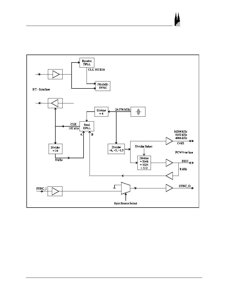
863C ]Y^Y
1eWecd " !
&) _V '(
Cologne
Chip
10
Clock synchronisation
10.1
Clock synchronisation in NT-mode
Figure 16: Clock synchronisation in NT-mode

863C ]Y^Y
' _V '(
1eWecd " !
Cologne
Chip
10.2
Clock synchronisation in TE-mode
Figure 17: Clock synchronisation in TE-mode
The C4IO clock is adjusted in the 31th time slot at the GCI/IOM bus 1..4 times for one half clock cycle.
This can be reduced to one adjustment of a half clock cycle (see MST_MODE1 register). This is useful if
another HFC series ISDN controller is connected as slave in NT mode to the PCM bus.
The SYNC source can be selected by the MST_MODE2 register settings.

863C ]Y^Y
1eWecd " !
'! _V '(
Cologne
Chip
10.3
Multiple HFC-S mini SYNC scheme
The SYNC scheme for multiple HFC-S mini ISDN controllers is shown in the figure below. The SYNC
source of the whole system can be selected by software (see also: MST_MODE2 register bit description).
Figure 18: Multiple HFC-S mini SYNC scheme

863C ]Y^Y
'" _V '(
1eWecd " !
Cologne
Chip
11
HFC-S mini package dimensions
Figure 19: HFC-S mini package dimensions

863C ]Y^Y
1eWecd " !
'# _V '(
Cologne
Chip
12
Sample circuitries
12.1
HFC-S mini in mode 2 (Motorola bus)
A
B
C
D
1
1
2
2
3
3
4
4
5
5
A
B
C
D
D2
D7
W
AKE_
U
P
D2
LEV_R
2
F0
I
O
F1
_
A
LEV_R
1
F1
_
B
to Moto
rola Pro
cesso
r
in
terfa
ce
D3
C5
33
n
HFC
S Min
i in
Mode
2
D6
R2
1M
TX
1
_
HI
/IN
T
GN
D
GN
D
D1
D0
D7
A0
C1
33
p
D6
Pr
ocess
or i
nter
face
sign
als
D5
/
T
X_EN
U1
B
HF
CS_
M
I
N
I
_
2
12
18
24
29
37
39
41
3
19
40
GN
D
GN
D
GN
D
GN
D
GN
D
GN
D
GN
D
VD
D
VD
D
VD
D
R1
R1
33
0
TX
2
_
HI
GN
D
C2
33
p
/R
E
S
R/
W
D3
/T
X
1
_
L
O
GN
D
GN
D
24
.
5
7
6
Q1
U1
A
HF
CS
_
M
I
N
I
_
2
26
27
38
43
4
5
6
7
8
9
10
11
47
1
2
36
45
44
46
48
28
25
23
22
21
20
17
16
15
14
13
34
35
32
33
31
30
CLK
I
CLK
O
S
Y
NC_
I
S
Y
NC_
O
D0
D1
D2
D3
D4
D5
D6
D7
A0
DS
RW
WA
I
T
AL
E
IN
T
CS
RE
S
AW
A
K
E
AD
J
_
L
E
V
R1
LE
V
_
R
1
LE
V
_
R
2
R2
TX
1
_
H
I
T
X
2_
LO
TX
_
E
N
T
X
1_
LO
TX
2
_
H
I
F
1_A
F
1_B
ST
I
O
1
ST
I
O
2
F0
I
O
C4
I
O
JP
1
1
3
5
7
9
11
13
15
17
19
2
4
6
8
10
12
14
16
18
20
R/
W
ST
I
O
1
GN
D
/D
S
D4
/T
X
2
_
L
O
R2
C6
33
n
AD
J
_
L
E
V
/W
A
I
T
1.
0
M
o
t
o
r
o
l
a
b
u
s
w
i
t
h
co
nt
r
o
l
si
g
n
a
l
s /
C
S
,
R
/
W
,
/
D
S
A4
11
T
u
esd
a
y
,
A
u
g
u
st
14
,
20
01
Ti
t
l
e
S
i
z
e
Do
c
u
m
e
n
t
Nu
m
b
e
r
Re
v
D
a
t
e
:
S
he
et
of
D0
SYN
C
_
O
A0
C4
I
O
D4
SYN
C
_
I
C4
33
n
/D
S
/I
N
T
/C
S
D1
ST
I
O
2
+
C3
10
�
D5
VD
D
GN
D
VD
D
/C
S

863C ]Y^Y
'$ _V '(
1eWecd " !
Cologne
Chip
A
B
C
D
1
1
2
2
3
3
4
4
5
5
A
B
C
D
/
T
X2
_LO
GN
D
Q5
/
T
X1
_LO
R3
D5
D1
RA
2
RE
1
RD2
RG
2
RG
1
RF
2
GN
D
GN
D
RC1
/
T
X_
EN
RB
2
R1
1
R1
R8
GN
D
C4
LE
V
_
R
1
R1
Q2
TR
1
A
RE
C
remote wake-up (optional)
If not used WAKE_UP pin
must be grounded.
R2
GN
D
VD
D
VD
D
TX
1
_
HI
Q1
Q3
R4
RA
1
W
AKE
_
U
P
RD1
RC2
RF
1
Q4
TR
1
B
TR
A
N
S
C7
R5
R2
TX
2
_
H
I
R6
D4
LE
V
_
R
2
C2
RB
1
D3
VD
D
D2
R9
I
S
DN_
S
T
1
RE
C1
RE
C2
TR
A
N
S
1
TR
A
N
S
2
GN
D
GN
D
AD
J
_
L
E
V
R7
C1
Q6
RE
2
GN
D
R1
2
C6
1.
0
A4
22
T
uesday
,
A
ugust
14,
2001
Ti
t
l
e
S
i
ze
D
o
cum
e
n
t
N
u
m
b
er
R
e
v
D
a
t
e
:
S
heet
of
HFCS
Mini i
n
Mode 2
M
o
t
o
r
o
l
a
bu
s w
i
t
h
c
ont
r
o
l
s
i
gnal
s
/
C
S
,
R
/
W
,
/
D
S

863C ]Y^Y
1eWecd " !
'% _V '(
Cologne
Chip
12.2
HFC-S mini in mode 3 (Intel bus with separated address bus/data bus)
A
B
C
D
1
1
2
2
3
3
4
4
5
5
A
B
C
D
VD
D
R2
W
AKE_
U
P
HFCS
Mi
ni in Mod
e
3
GN
D
JP
1
1
3
5
7
9
11
13
15
17
19
2
4
6
8
10
12
14
16
18
20
D7
A0
/R
E
S
Pro
ces
sor
in
ter
face
si
gna
ls
GN
D
SYN
C
_
I
F
1_B
D6
F0
I
O
D2
U1
B
HF
C
S
_
M
I
N
I
_
2
12
18
24
29
37
39
41
3
19
40
GN
D
GN
D
GN
D
GN
D
GN
D
GN
D
GN
D
VD
D
VD
D
VD
D
T
X
2_H
I
/R
D
/IN
T
C4
33n
D2
T
X
1_H
I
D0
C6
33n
/W
R
/C
S
C4
I
O
ST
I
O
2
GN
D
C1
33p
GN
D
U1
A
HF
CS
_
M
I
N
I
_
2
26
27
38
43
4
5
6
7
8
9
10
11
47
1
2
36
45
44
46
48
28
25
23
22
21
20
17
16
15
14
13
34
35
32
33
31
30
CL
K
I
CL
K
O
S
Y
NC_
I
S
Y
NC_
O
D0
D1
D2
D3
D4
D5
D6
D7
A0
RD
WR
WA
I
T
AL
E
IN
T
CS
RE
S
A
W
AKE
A
D
J
_LE
V
R1
LE
V
_
R1
LE
V
_
R2
R2
TX
1
_
H
I
T
X
2_LO
TX
_
E
N
T
X
1_LO
TX
2
_
H
I
F
1_A
F
1_B
ST
I
O
1
ST
I
O
2
F0
I
O
C4
I
O
C5
33
n
R1
/
T
X_
EN
D5
GN
D
A0
D4
D0
t
o
In
tel
no
n m
ulti
ple
xed
Pr
oce
sso
r i
nte
rfa
ce
L
EV_
R
2
L
EV_
R
1
R2
1M
D4
D1
ST
I
O
1
D7
GN
D
GN
D
D1
1.
0
I
n
t
e
l
bu
s
w
i
t
h
s
e
p
e
r
at
ed
ad
r
e
s
s
a
n
d
d
a
t
a
b
u
s
,
c
o
nt
r
o
l
s
i
gn
a
l
s
/
C
S,
/
W
R
,
/
R
D
A4
11
T
u
esday
,
A
ugust
14,
2
001
Ti
t
l
e
Si
z
e
Do
c
u
m
e
n
t
Nu
mb
e
r
Re
v
Da
t
e
:
S
h
e
e
t
of
/I
N
T
/
T
X2
_LO
D5
/R
D
D3
R1
330
C2
33p
/
T
X1
_LO
D3
24.
5
7
6
Q1
GN
D
A
D
J
_LE
V
/W
A
I
T
+
C3
10�
D6
/C
S
F
1_A
/W
R
SYN
C
_
O

863C ]Y^Y
'& _V '(
1eWecd " !
Cologne
Chip
A
B
C
D
1
1
2
2
3
3
4
4
5
5
A
B
C
D
/
T
X2
_LO
GN
D
Q5
/
T
X1
_LO
R3
D5
D1
RA
2
RE
1
RD2
RG
2
RG
1
RF
2
GN
D
GN
D
RC1
/
T
X_
EN
RB
2
R1
1
R1
R8
GN
D
C4
LE
V
_
R
1
R1
Q2
TR
1
A
RE
C
remote wake-up (optional)
If not used WAKE_UP pin
must be grounded.
R2
GN
D
VD
D
VD
D
TX
1
_
HI
Q1
Q3
R4
RA
1
W
AKE
_
U
P
RD1
RC2
RF
1
Q4
TR
1
B
TR
A
N
S
C7
R5
R2
TX
2
_
H
I
R6
D4
LE
V
_
R
2
C2
RB
1
D3
VD
D
D2
R9
I
S
DN_
S
T
1
RE
C1
RE
C2
TR
A
N
S
1
TR
A
N
S
2
GN
D
GN
D
AD
J
_
L
E
V
R7
C1
Q6
RE
2
GN
D
R1
2
C6
HFCS M
ini in
Mode
3
1.
0
I
n
t
e
l
bus w
i
t
h
seper
at
ed
adr
ess
and
dat
a b
u
s,
cont
r
o
l
si
gnal
s /
C
S
,
/
W
R
,
/
R
D
A4
22
T
uesday
,
A
ugust
14,
2001
Ti
t
l
e
S
i
ze
D
o
cum
e
n
t
N
u
m
b
er
R
e
v
D
a
t
e
:
S
heet
of

863C ]Y^Y
1eWecd " !
'' _V '(
Cologne
Chip
12.3
HFC-S mini in mode 4 (Intel bus with multiplexed address bus/data bus)
A
B
C
D
1
1
2
2
3
3
4
4
5
5
A
B
C
D
R2
1M
D6
C6
33n
ST
I
O
1
/W
R
1.
0
I
n
t
e
l
bu
s
w
i
t
h
m
u
l
t
i
p
l
e
x
e
d ad
dr
e
s
s a
n
d
da
t
a
bus
A4
11
T
u
e
s
d
a
y
,
A
u
gu
st
14
,
20
01
Ti
t
l
e
Si
z
e
Do
c
u
me
n
t
Nu
mb
e
r
Re
v
D
a
t
e
:
S
he
et
of
/C
S
R1
D2
GN
D
Pr
ocessor int
erface signal
s
/R
D
/W
A
I
T
C2
33p
/W
R
D3
AL
E
D2
TX
1
_
H
I
AL
E
R2
F0
I
O
ST
I
O
2
JP
1
1
3
5
7
9
11
13
15
17
19
2
4
6
8
10
12
14
16
18
20
D7
D5
/T
X
_
E
N
GN
D
/R
D
to Intel mul
tiplexed P
rocessor inter
face
L
EV_R
2
GN
D
GN
D
/
T
X
2_L
O
D0
/R
E
S
TX
2
_
H
I
D4
F1
_
B
C1
33p
C5
33
n
D0
F1
_
A
/I
N
T
U1
B
H
F
C
S
_
M
IN
I_
2
12
18
24
29
37
39
41
3
19
40
GN
D
GN
D
GN
D
GN
D
GN
D
GN
D
GN
D
VD
D
VD
D
VD
D
/
T
X
1_L
O
D1
D1
D4
R1
33
0
D5
D7
C4
33
n
HFCS Mini
in Mode 4
S
Y
NC_
I
GN
D
GN
D
D3
/I
N
T
D6
L
EV_R
1
U1
A
H
F
C
S
_
M
IN
I_
2
26
27
38
43
4
5
6
7
8
9
10
11
47
1
2
36
45
44
46
48
28
25
23
22
21
20
17
16
15
14
13
34
35
32
33
31
30
CL
K
I
CL
K
O
SY
N
C
_
I
SY
N
C
_
O
D0
D1
D2
D3
D4
D5
D6
D7
A0
RD
WR
WA
I
T
AL
E
IN
T
CS
RE
S
AW
A
K
E
AD
J
_
L
E
V
R1
LEV
_
R
1
LEV
_
R
2
R2
T
X
1_H
I
T
X
2_
LO
TX
_
E
N
T
X
1_
LO
T
X
2_H
I
F1
_
A
F1
_
B
ST
I
O
1
ST
I
O
2
F0
I
O
C4
I
O
S
Y
NC_
O
AD
J
_
LEV
C4
I
O
+
C3
10
�
GN
D
VD
D
W
AKE
_
U
P
/C
S
2
4
.
576
Q1
GN
D

863C ]Y^Y
'( _V '(
1eWecd " !
Cologne
Chip
A
B
C
D
1
1
2
2
3
3
4
4
5
5
A
B
C
D
/
T
X
2
_LO
GN
D
Q5
/
T
X1_LO
R3
D5
D1
RA
2
RE
1
RD2
RG
2
RG
1
RF2
GN
D
GN
D
RC1
/
T
X_EN
RB
2
R1
1
R1
R8
GN
D
C4
LEV
_
R
1
R1
Q2
TR
1
A
RE
C
remot
e wak
e-up
(opt
ional
)
If no
t use
d WA
KE_UP
pin
must be
gr
ound
ed.
R2
GN
D
VD
D
VD
D
T
X
1_H
I
Q1
Q3
R4
RA
1
WA
K
E
_
U
P
RD1
RC2
RF
1
Q4
TR
1
B
TR
A
N
S
C7
R5
R2
TX
2
_
H
I
R6
D4
LEV
_
R
2
C2
RB
1
D3
VD
D
D2
R9
I
S
DN_
S
T
1
RE
C1
RE
C2
TRA
N
S
1
TRA
N
S
2
GN
D
GN
D
AD
J
_
L
E
V
R7
C1
Q6
RE
2
GN
D
R1
2
C6
4
5
I
n
t
e
l
bus
w
i
t
h
m
u
l
t
i
p
l
e
x
e
d
ad
dr
es
s
a
nd d
a
t
a
b
u
s
HFCS
Mini in Mo
de 4
1.
0
A4
22
T
u
esd
a
y
,
A
u
g
u
st
14,
20
01
Ti
t
l
e
S
i
z
e
Do
c
u
m
e
n
t
Nu
m
b
e
r
Re
v
D
a
t
e
:
S
he
et
of