 | –≠–ª–µ–∫—Ç—Ä–æ–Ω–Ω—ã–π –∫–æ–º–ø–æ–Ω–µ–Ω—Ç: CZRB2082 | –°–∫–∞—á–∞—Ç—å:  PDF PDF  ZIP ZIP |
Voltage: 11 - 100 Volts
Power: 2.0 Watt
CZRB2011 Thru CZRB2100
Features
- For surf ace mounted applications in order to
optimize board space
- Low profile package
- Built-in strain relief
- Glass passivated junction
- Low inductance
- Excellent clamping capability
- Typical I less than 1uA above 11V
D
- High temperature soldering 260∞C /10
seconds at terminals
- Plastic package has underwriters laboratory
flammability classification 94V-O
Mechanical data
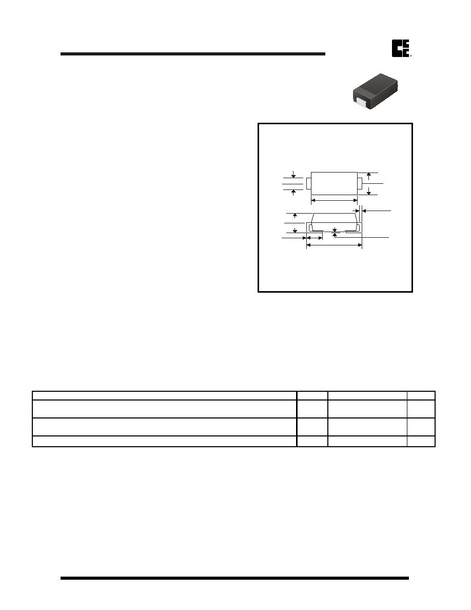
- Case: JEDEC DO-214AA, Molded plastic
over passivated junction
- Terminals: Solder plated, solderable per MIL-
STD-750, method 2026
- Polarity: Color band denotes positive end
(cathode) except Bidirectional
- Standard Packaging: 12mm tape (EIA-481)
- Weight: 0.002 ounce, 0.064 gram
Surface Mount Zener Diode
www.comchip.com.tw
COMCHIP
COMCHIP
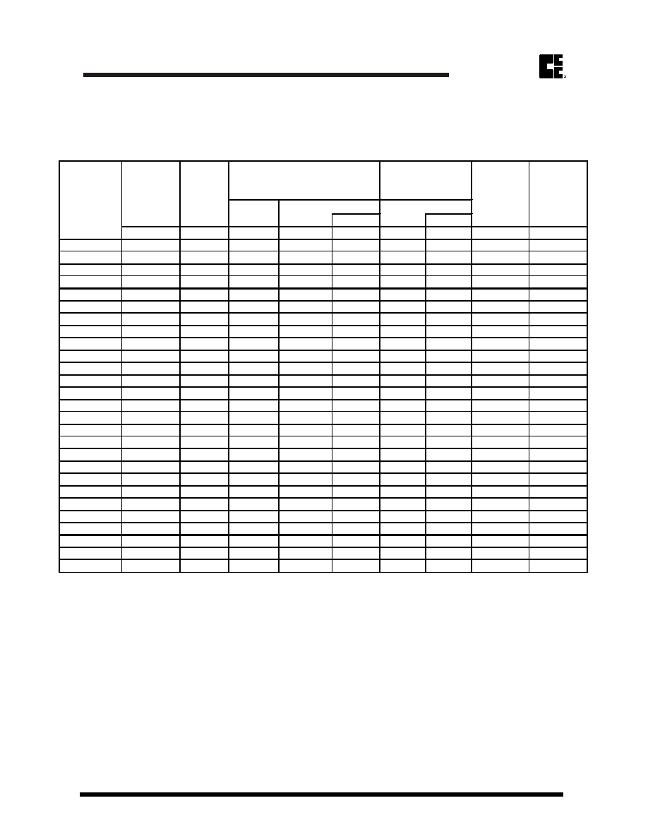
Maximum Ratings and Electrical Characterics
MDS0302004A
Page 1
Rating
Symbol
Value
Units
Peak Pulse Power Dissipation (Note A)
2
Watts
Derate above 75∞C
24
mW/∞C
Peak forward Surge Current 8.3ms single half s ine-wave superimposed
on rated load (JEDEC Method) (Note B)
Operating Junction and Storage Temperature Range
T
J
,T
STG
-55 to +150
∞C
P
D
15
Amps
Ratings at 25∞C ambient temperature unless otherwise specified.
I
FSM
SMB/DO-214AA
Dimensions in inches and (maillimeter)
0.008(0.20)
0.203(0.10)
0.083(2.11)
0.075(1.91)
0.096(2.44)
0.083(2.13)
0.050(1.27)
0.030(0.76)
0.155(3.94)
0.130(3.30)
0.185(4.70)
0.160(4.06)
0.012(0.31)
0.006(0.15)
0.220(5.59)
0.200(5.08)
www.comchip.com.tw
COMCHIP
COMCHIP
MDS0302004A
Page 2
Surface Mount Zener Diode
Rating and Characteristic Curevs (CZRB2011 Thru CZRB2100)
I
ZK
V
R
(Volts)
(mA)
(Ohms)
(Ohms)
(mA)
(uA)
(Volts)
(mA)
Ir - mA
CZRB2011
11
45.5
4
700
0.25
1.0
8.4
166
1.82
CZRB2012
12
41.5
4.5
700
0.25
1.0
9.1
152
1.66
CZRB2013
13
38.5
5
700
0.25
0.5
9.9
138
1.54
CZRB2014
14
35.7
5.5
700
0.25
0.5
10.6
130
1.43
CZRB2015
15
33.4
7
700
0.25
0.5
11.4
122
1.33
CZRB2016
16
31.2
8
700
0.25
0.5
12.2
114
1.25
CZRB2017
17
29.4
9
750
0.25
0.5
13
107
1.18
CZRB2018
18
27.8
10
750
0.25
0.5
13.7
100
1.11
CZRB2019
19
26.3
11
750
0.25
0.5
14.4
95
1.05
CZRB2020
20
25
11
750
0.25
0.5
15.2
90
1.00
CZRB2022
22
22.8
12
750
0.25
0.5
16.7
82
0.91
CZRB2024
24
20.8
13
750
0.25
0.5
18.2
76
0.83
CZRB2027
27
18.5
18
750
0.25
0.5
20.6
68
0.74
CZRB2030
30
16.6
20
1000
0.25
0.5
22.5
60
0.67
CZRB2033
33
15.1
23
1000
0.25
0.5
25.1
55
0.61
CZRB2036
36
13.9
25
1000
0.25
0.5
27.4
50
0.56
CZRB2039
39
12.8
30
1000
0.25
0.5
29.7
47
0.51
CZRB2043
43
11.6
35
1500
0.25
0.5
32.7
43
0.45
CZRB2047
47
10.6
40
1500
0.25
0.5
35.6
39
0.42
CZRB2051
51
9.8
48
1500
0.25
0.5
38.8
36
0.39
CZRB2056
56
9
55
2000
0.25
0.5
42.6
32
0.36
CZRB2062
62
8.1
60
2000
0.25
0.5
47.1
29
0.32
CZRB2068
68
7.4
75
2000
0.25
0.5
51.7
27
0.29
CZRB2075
75
6.7
90
2000
0.25
0.5
56
24
0.27
CZRB2082
82
6.1
100
3000
0.25
0.5
62.2
22
0.24
CZRB2091
91
5.5
125
3000
0.25
0.5
69.2
20
0.22
CZRB2100
100
5
175
3000
0.25
0.5
76
18
0.20
NOTE:
ELECTRICAL CHARACTERISTICS
(T
A
=25∞C unless otherwise noted) (V
F
=1.2Volts Max, I
F
=500mA for all types.)
Device
(Note 1.)
Nominal
Zener
Voltage V
Z
@ I
ZT
(Note 2.)
Test
current
I
ZT
Maximum Zener Impedance
(Note 3.)
Leakage Current
Surge
Current
@T
A
=25∞C
(Note 4.)
Z
ZT
@ I
ZT
Z
ZK
@ I
ZK
I
R
Maximum
Zener
Current I
ZM
1. TOLERANCES - Suffix indicates 5% tol erance any other tolerance will be considered as a special devic e.
2. ZENER VOLTAGE (Vz) MEASUREMENT - guarantees the zener voltage when m easured at 40 ms ± 10ms
from the diode body, and an ambient temperat ure of 25 ∞C (+ 8 ∞C , -2 ∞C ).
3.ZENER IMPEDANCE (Zz) DERIVATION - The zener im pedance is derived from the 60 cycle ac voltage,
which results when an ac current having an rms falue equal to 10% of the dc zener current (I
ZT
or I
ZK
) is
superimposed on I
ZT
or I
ZK
.
4. SURGE CURRENT (Ir) NON-REPETITIVE - The rating li sted in the electrical characteris tics table is
maximum peak, non-repetitive, reverse surge c urrent of 1/2 square wave or equivalent sine wave pulse
of 1/120 second duration superimposed on the tes t current, I
ZT
, per JEDEC standards, however, actual
device capability is as described in Figure 3.
Rating and Characteristic Curves (CZRB2011 Thru CZRB2100)
www.comchip.com.tw
COMCHIP
MDS0302004A
Page 3
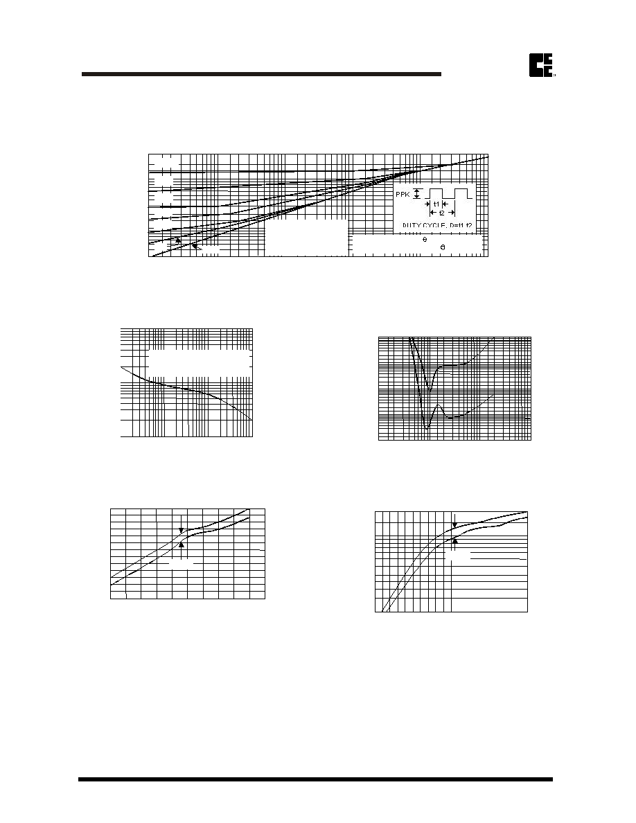
Surface Mount Zener Diode
30
20
10
7
5
3
2
1
0.7
0.5
0.3
0.0001 0.0002
0.0005 0.001 0.002
0.005
0.01
0.02
0.05
0.1
0.2
0.5
1
2
5
10
D = 0.5
0.2
0.1
0.05
0.02
0.01
D = 0
NOTE BELOW 0.1 SECOND,
THERMAL RESPONSE
CURVE IS APPLICABLE TO
ANY LEAD LENGTH (L)
SINGLE PULSE
TJL =
JL(t)PPK
REPETITIVE PULSES
TJL =
JL(t,D)PPK
Fig. 2-TYPICAL THERMAL RESPONSE L,
1K
500
300
200
100
50
30
20
10
.1 .2 .3 5 1
2 3 5 10 20
50 100
RECTANGULAR NONREPETITIVE
WAVEFORM TJ = 25∞C PRIOR TO
INITIAL PULSE
P.W. PULSE WIDTH (ms)
0.1
0.05
0.03
0.02
0.01
0.005
0.003
0.002
0.001
0.0005
0.0003
0.0002
0.0001
1
2
5
10
20
50
100
200
500
1K
NOMINAL VZ (VOLTS)
Fig. 3-MAXIMUM SURGE POWER
Fig. 4-TYPICAL REVERSE LEAKAGE
8
6
4
2
0
-2
-4
3 4 6 8 10 12
RANGE
VZ, ZENER VOLTAGE @IZT (VOLTS)
200
100
50
40
30
20
10
0
20
40
60
80
100
RANGE
VZ, ZENER VOLTAGE @IZT (VOLTS)
Fig. 5 - UNITS TO 12 VOLTS
Fig. 6 - UNITS 10 TO 100 VOLTS
TRAN
SIEN
T
T
H
ERM
AL
RES
IST
ANCE
JU
NCTI
ON-
TO
-LEA
D(∞C
/W
)
PPK
, PE
AK S
URG
E PO
W
E
R(WA
TTS
)
IR,
REV
ERSE
LEA
DAG
E(uA
dc)
@
VR A
S
SP
ECIF
IED
IN E
LEC.
CHAR
. T
ABLE
T
E
M
PERA
TUR
E
CO
EFFI
CIEN
T(mV
/∞C
)
@
I
Z
T
TEM
PE
RA
T
URE
C
OEF
FICI
ENT(
mV/
∞C)
@
IZT
Rating and Characteristic Curves (CZRB2011 Thru CZRB2100)
www.comchip.com.tw
COMCHIP
MDS0302004A
Page 4
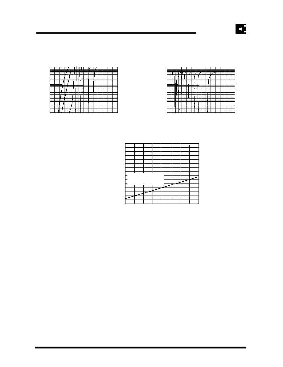
Surface Mount Zener Diode
100
50
30
20
10
5
3
2
1
0.5
0.3
0.2
0.1
0 1 2 3 4 5 6 7 8 9 10
VZ, ZENER VOLTAGE (VOLTS)
100
50
30
20
10
5
3
2
1
0.5
0.3
0.2
0.1
0 10 20 30 40 50 60 70 80 90 100
VZ, ZENER VOLTAGE (VOLTS)
80
70
60
50
40
30
20
10
0
0 1/8 1/4 3/8 1/2 5/8 3/4 7/8 1
PRIMARY PATH OF
CONDUCTION IS THROUGH
THE CATHODE LEAD
L, LEAD LENGTH TO HEAT SINK (INCH)
Fig. 9 -TYPICAL THERMAL RESISTANCE
I
Z, Z
ENER
CUR
RENT
(mA
)
JUN
CTIO
N-L
EAD
THER
MA
L
RES
IST
ANCE
(∞C/W
)

APPLICATION NOTE:
Since the actual voltage available from a given zener
diode is temperature dependent, it is necessary to
determine junction temperature under any set of
operating conditions in order to calculate its value. The
following procedure is recommended:
Lead Temperature, T
L
, should be determined from:
T
L
=
LA
P
D
+ T
A
LA
is the lead-to-ambient thermal resistance (∞C/W)
and PD is the power dissipation. The value for
LA
will
vary and depends on the device mounting method.
LA
is generally 30-40 ∞C/W for the various chips and
tie points in common use and for printed circuit board
wiring.
The temperature of the lead can also be measured using
a thermocouple placed on the lead as close as possible to
the tie point. The thermal mass connected to the tie point
is normally large enough so that it will not significantly
respond to heat surges generated in the diode as a result
of pulsed operation once steady-state conditions are
achieved. Using the measured value of T
L
, the junction
temperature may be determined by:
T
J
= T
L
+ T
JL
T
JL
is the increase in junction temperature above the
lead temperature and may be found from Figure 2 for a
train of power pulses or from Figure 10 for dc power.
T
JL
=
LA
P
D
For worst-case design, using expected limits of Iz, limits
of PD and the extremes of TJ ( T
JL
) may be estimated.
Changes in voltage, Vz, can then be found from:
V =
VZ
T
J
VZ
, the zener voltage temperature coefficient, is
found from Figures 5 and 6.
Under high power-pulse operation, the zener voltage
will vary with time and may also be affected significantly
be the zener resistance. For best regulation, keep current
excursions as low as possible.
Data of Figure 2 should not be used to compute surge
capability. Surge limitations are given in Figure 3. They
are lower than would be expected by considering only
junction temperature, as current crowding effects cause
temperatures to be extremely high in small spots resulting
in device degradation should the limits of Figure 3 be
exceeded.
www.comchip.com.tw
COMCHIP
MDS0302004A
Page 5
Surface Mount Zener Diode