 | ÐлекÑÑоннÑй компоненÑ: CZRW5230 | СкаÑаÑÑ:  PDF PDF  ZIP ZIP |
Äîêóìåíòàöèÿ è îïèñàíèÿ www.docs.chipfind.ru
Voltage: 2.4 - 39 Volts
Power
: 500mW
CZRW5221 - CZRW5259
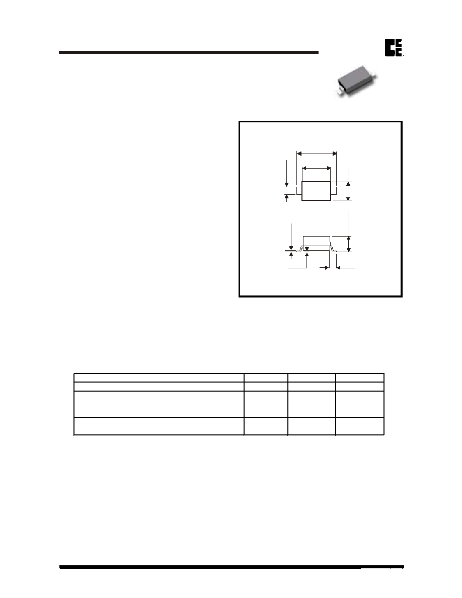
Dimensions in inches and (millimeters)
SOD-123
MDS0208005A
Page 1
.154 (3.90)
.016 (.40)Min.
.005 (.12) MAX.
.098 (2.50)
.110 (2.80)
.141 (3.60)
.
037(0.95)
.
053(1.35)
.
008(0.20)
Max.
.
055(1.40)
.
071(1.80)
.
019(0.50)
.
028(0.70)
NOTES:
A. Mounted on 5.0mm
2
(.013mm thick) land areas.
B. Measured on 8.3ms, single half sine-wave or equivalent square wave, duty cycle = 4 pulses per minute maximum.
Parameter
Symbol
Value
Units
Power Dissipation (Note A) at 75°C
PD
500
mW
Peak Forward Surge Current Surge, 8.3ms Single
Half Sine-wave Superimposed on Rated Load
(JEDEC Method) (Note B)
IFSM
4
A
Operating Junction and Storage Temperature Range
TJ
-55 to +150
°C
Maximum Ratings and Electrical Characterics
Planar Die constructions
500mW Power Dissipation
Zener Voltages from 2.4V - 39V
Ideally Suited for Automated Assembly Processes
Case: SOD-123, Molded Plastic
Terminals: Solderable per MIL-STD-202, Method 208
Polarity: See Diagram Below
Approx. Weight: 0.008 grams
Mounting Position: Any
FEATURES
MECHANICAL DATA
www.comchip.com.tw
COMCHIP
Surface Mount Zener Diodes
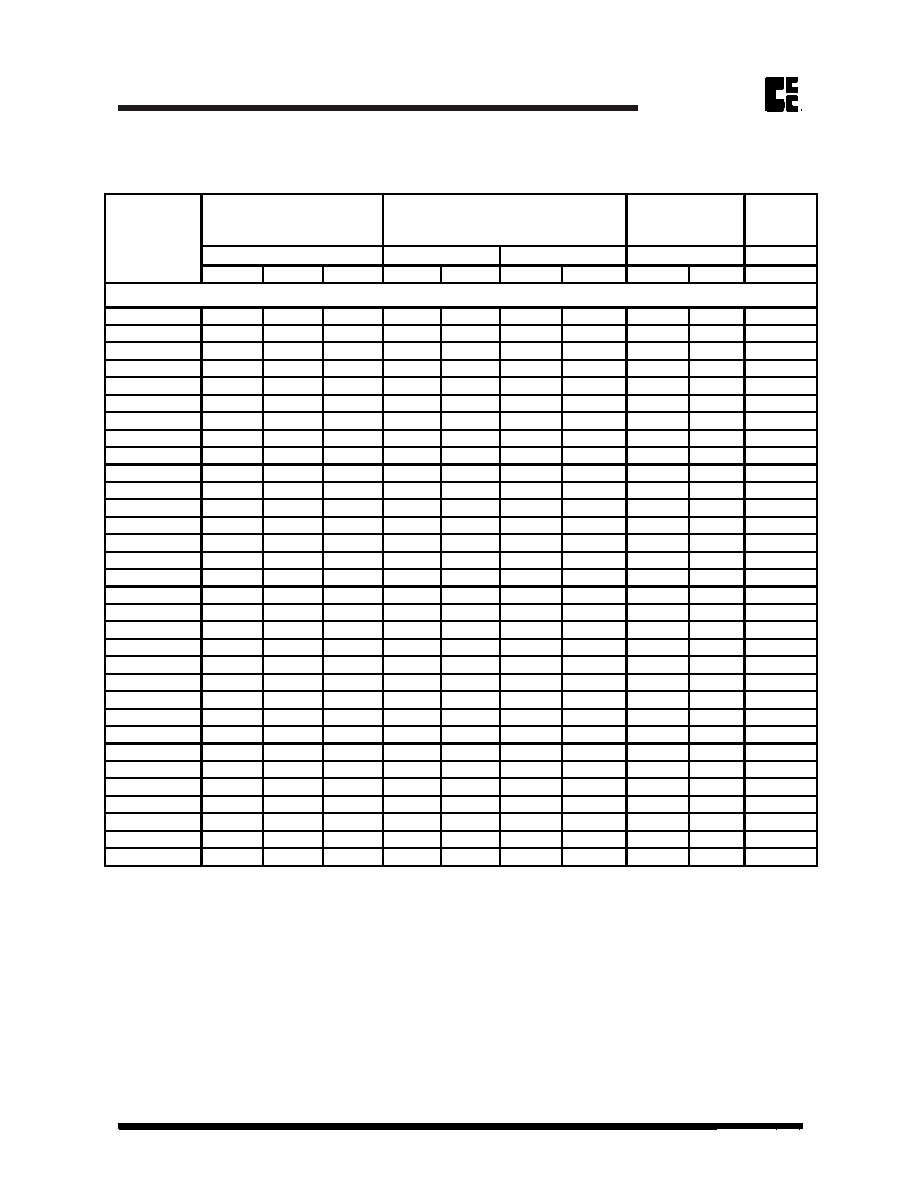
NOTE:
1. Tolerance and Type Number Designation. The type numbers listed have a standard tolerance on the nominal zener voltage of ±5%.
2. Specials Available Include:
A. Nominal zener voltages between the voltages shown and tighter voltage tolerances.
B. Matched sets.
3. Zener Voltage (V
Z
) Measurement. Guarantees the zener voltage when measured at 90 seconds while maintaining the lead temperature (T
L
) at 30
O
C, from the diode body.
4. Zener Impedance (Z
Z
) Derivation. The zener impedance is derived from the 60 cycle ac voltage, which results when an AC current having an rms value equal to 10% of the dc zener
current (I
ZT
or I
ZK
) is superimposed on I
ZT
or I
ZK
.
5. Surge Current (I
R
) Non-Repetitive. The rating listed in the electrical characteristics table is maximum peak, non-repetitive, reverse surge current of 1/2 square wave or equivalent sine
wave pulse of 1/120 second duration superimposed on the test current, I
ZT
, per JEDEC registration; however, actual device capability is as described in Figure 5.
MDS0208005A
Page 2
www.comchip.com.tw
I
ZM
@ T
A
Nom. V
Min. V
Max. V
Ohm
mA
Ohm
mA
nA
V
mA
CZRW5221
2.4
2.28
2.52
30
20
1200
0.25
100
1
188
CZRW5222
2.5
2.38
2.63
30
20
1250
0.25
100
1
180
CZRW5223
2.7
2.57
2.84
30
20
1300
0.25
75
1
167
CZRW5225
3
2.85
3.15
30
20
1600
0.25
50
1
150
CZRW5226
3.3
3.14
3.47
28
20
1600
0.25
25
1
138
CZRW5227
3.6
3.42
3.78
24
20
1700
0.25
15
1
126
CZRW5228
3.9
3.71
4.1
23
20
1900
0.25
10
1
115
CZRW5229
4.3
4.09
4.52
22
20
2000
0.25
5
1
106
CZRW5230
4.7
4.47
4.94
19
20
1900
0.25
5
2
97
CZRW5231
5.1
4.85
5.36
17
20
1600
0.25
5
2
89
CZRW5232
5.6
5.32
5.88
11
20
1600
0.25
5
3
81
CZRW5234
6.2
5.89
6.51
7
20
1000
0.25
5
4
73
CZRW5235
6.8
6.46
7.14
5
20
750
0.25
3
5
67
CZRW5236
7.5
7.13
7.88
6
20
500
0.25
3
6
61
CZRW5237
8.2
7.79
8.61
8
20
500
0.25
3
6
55
CZRW5239
9.1
8.65
9.56
10
20
600
0.25
3
6.5
50
CZRW5240
10
9.5
10.5
17
20
600
0.25
3
8
45
CZRW5241
11
10.45
11.55
22
20
600
0.25
3
8.4
41
CZRW5242
12
11.4
12.6
30
2 0
600
0.25
2
9.1
3 8
CZRW5243
13
12.35
13.65
13
9.5
600
0.25
1
9.9
35
CZRW5245
15
14.25
15.75
16
8.5
600
0.25
0.5
11
30
CZRW5246
16
15.2
16.8
17
7.8
600
0.25
0.1
12
28
CZRW5248
18
17.1
18.9
21
7
600
0.25
0.1
14
25
CZRW5250
20
19
21
25
6.2
600
0.25
0.1
15
23
CZRW5251
22
20.9
23.1
29
5.6
600
0.25
0.1
17
21
CZRW5252
24
22.8
25.2
33
5.2
600
0.25
0.1
18
19.1
CZRW5254
27
25.65
28.35
41
5
600
0.25
0.1
21
16.8
CZRW5255
28
26.6
29.4
44
4.5
600
0.25
0.1
21
16.2
CZRW5256
30
28.5
31.5
49
4.2
600
0.25
0.1
23
15.1
CZRW5257
33
31.35
34.65
58
3.8
700
0.25
0.1
25
13.8
CZRW5258
36
34.2
37.8
70
3.4
700
0.25
0.1
27
12.6
CZRW5259
39
37.05
40.95
80
3.2
800
0.25
0.1
30
11.6
Max Reverse
Leakage Current
Max
Zener
Current
Maximum Ratings and Electrical Characterics
(TA=25 unless otherwise noted) VF=1.2V, IF=100m A for all types
500 mWatts Zener Diodes
V
Z
@ I
ZT
Z
ZT
@ I
ZT
Z
ZK
@ I
ZK
Max. Zener Impedance
Nominal Zener Voltage
Part Number
I
R
@ V
R
NOTE:
1. Tolerance and Type Number Designation. The type numbers listed have a standard tolerance on the nominal zener voltage of ±5%.
2. Specials Available Include:
A. Nominal zener voltages between the voltages shown and tighter voltage tolerances.
B. Matched sets.
3. Zener Voltage (V
Z
) Measurement. Guarantees the zener voltage when measured at 90 seconds while maintaining the lead temperature (T
L
) at 30
O
C, from the diode body.
4. Zener Impedance (Z
Z
) Derivation. The zener impedance is derived from the 60 cycle ac voltage, which results when an AC current having an rms value equal to 10% of the dc zener
current (I
ZT
or I
ZK
) is superimposed on I
ZT
or I
ZK
.
5. Surge Current (I
R
) Non-Repetitive. The rating listed in the electrical characteristics table is maximum peak, non-repetitive, reverse surge current of 1/2 square wave or equivalent sine
wave pulse of 1/120 second duration superimposed on the test current, I
ZT
, per JEDEC registration; however, actual device capability is as described in Figure 5.
MDS0208005A
Page 2
Surface Mount Zener Diodes
www.comchip.com.tw
COMCHIP
MDS0208005A
Page 3
Surface Mount Zener Diodes
Surface Mount Zener Diodes
COMCHIP
COMCHIP
www.comchip.com.tw
COMCHIP
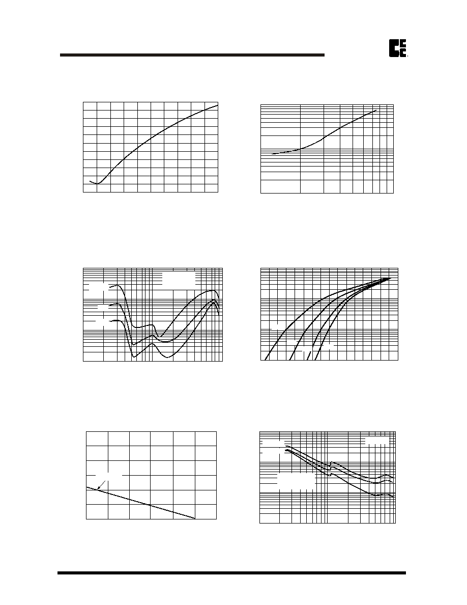
TYPICAL REVERSE CURRENT
TEMPERA
TURE
COEFFICIENT
,mV
/
C
)
o
NOMINAL ZENER VOLTAGE, Volts
-1
0
1
2
3
4
5
6
7
8
12
11
10
9
8
7
6
5
4
3
2
-2
-3
STEADY STATE POWER DERATING
100
10
1
1000
100
10
1
IZ = 1 mA
5 mA
20 mA
DYNAMIC
I
MPEDANCE,
W
NORMAL ZENER VOLTAGE, Volts
T
J
=25 C
O
I
Z(AC)=0.1
I
F=1 kHZ
Z(DC)
FOR
W
ARD
CURRENT
,m
A
1.2
1.1
1.0
0.9
0.8
0.7
0.6
0.5
0.4
1000
100
10
1
75 C
O
5 C
O
25 C
O
150 C
O
CAP
ACIT
ANCE,
pF
NOMINAL ZENER VOLTAGE, Volts
T =25 C
A
o
100
10
1
NOMINAL ZENER VOLTAGE, Volts
TEMPERA
TURE
COEFFICIENT
,mV
/
C
)
o
10
100
TYPICAL CAPACITANCE
100
1000
100
10
1
10
1
BIAS AT
50% OF VZ NOM
0 V BIAS
1 V BIAS
CAP
ACIT
ANCE,
pF
T =25 C
A
o
100
10
1
NOMINAL ZENER VOLTAGE, Volts
TEMPERA
TURE
COEFFICIENT
,mV
/
C
)
o
TEMPERATURE ( C)
o
POWER
DISSIP
A
TION,
W
atts
STEADY STATE POWER DERATING
1.2
1.0
0.8
0.6
0.4
0.2
0
150
125
100
75
50
25
P
D V
.
S
. T
A
155
TYPICAL FORWARD VOLTAGE
FORWARD VOLTAGE, Volts
MDS0208005A
Page 4
Surface Mount Zener Diodes
Surface Mount Zener Diodes
COMCHIP
COMCHIP
www.comchip.com.tw
COMCHIP
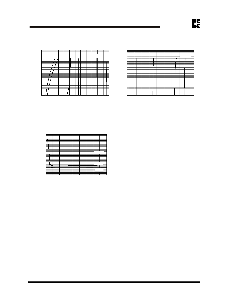
ZENER VOLTAGE V.S. ZENER CURRENT
TYPICAL LEAKGE CURRENT
90
1000
100
10
1
0.1
0.01
0.001
0.0001
0.00001
80
70
60
50
40
30
20
10
0
LEAKAGE
CURRENT
(
A)
m
NOMINAL ZENER VOLTAGE, Vlots
+150 C
O
+25 C
O
-55 C
O
12
100
10
1
0.1
0.01
10
8
6
4
2
0
ZENER
CURRENT
,m
A
ZENER VOLTAGE, Volts
T =25 C
A
o
100
10
1
0.1
0.01
10
30
50
70
90
T =25 C
A
o
ZENER VOLTAGE, Volts
ZENER VOLTAGE V.S. ZENER CURRENT
ZENER
CURRENT
,m
A