G
∑
SiC
Æ
Technology
SuperBrightTM LEDs
CXXX-CB290-S0100
Features Applications
∑ High Performance
≠ 2.0mW (460nm) Deep Blue
≠ 2.0mW (470nm) Blue
≠ 1.5mW (505nm) Signal Green
≠ 1.0mW (527nm) Green
∑ Sorted to Wavelength and Power Bins
∑ Single Wire Bond Structure
∑ Class II ESD Rating
∑ Outdoor LED Video Displays
∑ White LEDs
∑ Automotive Dashboard Lighting
∑ Cellular Phone Backlighting
∑ Audio Product Display Lighting
∑ Entertainment and Amusement
Description
Cree's CBTM series of SuperBrightTM LEDs combine highly efficient InGaN materials with Cree's
proprietary SiC substrate to deliver excellent price performance for high intensity blue and green LEDs.
These LED chips have an industry-standard vertical chip structure, which requires only a single wire bond
connection. Sorted Die Kits provide die sheets conveniently sorted into wavelength and radiant flux bins.
Cree's CB series chips are tested for conformity to optical and electrical specifications and the ability to
withstand 1000V ESD. These LEDs are useful in a broad range of applications such as outdoor and
indoor full motion LED video signs, transportation signaling and white LEDs, yet can also be used in high
volume applications such as LCD backlighting. Cree's CB series chips are compatible with most radial
and SMT LED assembly processes.
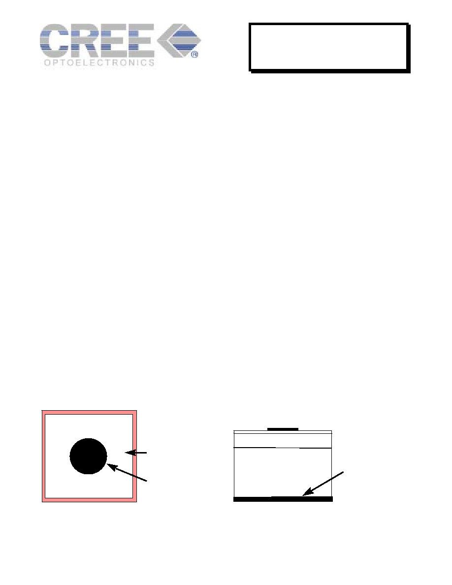
CXXX-CB290-S0100 Chip Diagram
Topside View
G
∑
SiCÆ LED Chip
300 x 300 µm
Mesa (junction)
240 x 240 µm
Gold Bond Pad
120 µm Diameter
Anode (+)
Die Cross Section
h = 250 µm
Backside
Metallization
Cathode (-)
InGaN
SiC Substrate
CPR3U Rev. I
© 1998-2003 Cree, Inc. All Rights Reserved.
G
∑
SiC
Æ
Technology
SuperBrightTM LEDs
CXXX-CB290-S0100
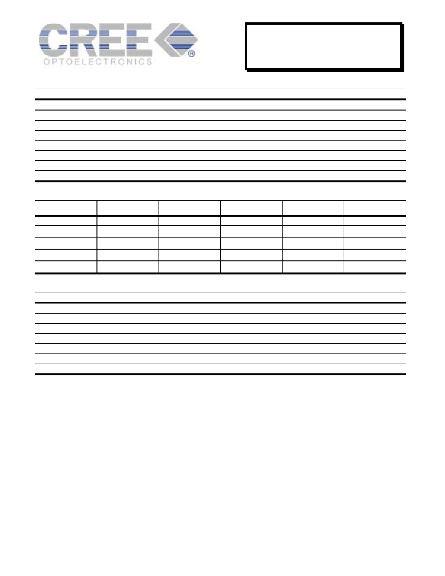
Maximum Ratings at T
A
= 25∞C
Notes 1&3
CXXX-CB290-S0100
DC Forward Current
30 mA
Peak Forward Current (1/10 duty cycle @ 1kHz)
100 mA
LED Junction Temperature
125∞C
Reverse Voltage
5 V
Operating Temperature Range
-20∞C to +80∞C
Storage Temperature Range
-30∞C to +100∞C
Electrostatic Discharge Threshold (HBM)
Note 2
1000
V
Electrostatic Discharge Classification (MIL-STD-883E)
Note 2
Class
2
Typical Electrical/Optical Characteristics at T
A
= 25∞C, If = 20mA
Note 3
Part Number
Forward Voltage
(V
f,
V)
Reverse Current
[I(Vr=5V), µA]
Peak Wavelength
(
p,
nm)
Halfwidth
(
D,
nm)
Optical Rise Time
(
, ns)
Typ
Max
Max Typ Typ Typ
C460CB290-S0100
3.3 3.7
10
458
26
30
C470CB290-S0100
3.3 3.7
10
468
26
30
C505CB290-S0100
3.3 3.7
10
502
30
30
C525CB290-S0100
3.3 3.7
10
523
36
30
Mechanical Specifications
CXXX-CB290-S0100
Description Dimension
Tolerance
P-N Junction Area (µm)
240 x 240
± 25
Bottom Area (µm)
300 x 300
± 25
Chip Thickness (µm)
250
± 25
Au Bond Pad Diameter (µm)
120
± 20
Au Bond Pad Thickness (µm)
1.2
± 0.5
Back Contact Metal Width (µm)
19.8
-5,+10
Notes:
1) Maximum ratings are package dependent. The above ratings were determined using a T-1 3/4 package (with Hysol OS4000 epoxy) for characterization.
Ratings for other packages may differ. The forward currents (DC and Peak) are not limited by the die but by the effect of the LED junction temperature on
the package. The junction temperature limit of 125∞C is a limit of the T-1 3/4 package; junction temperature should be characterized in a specific package to
determine limitations. Assembly processing temperature must not exceed 325∞C (< 5 seconds).
2) Product resistance to electrostatic discharge (ESD) according to the HBM is measured by simulating ESD using a rapid avalanche energy test (RAET). The
RAET procedures are designed to approximate the maximum ESD ratings shown. The RAET procedure is performed on each die. The ESD classification
of Class II is based on sample testing according to MIL-STD 883E.
3) All Products conform to the listed minimum and maximum specifications for electrical and optical characteristics, when assembled and operated at 20 mA
within the maximum ratings shown above. Efficiency decreases at higher currents. Typical values given are within the range of average values expected by
the manufacturer in large quantities and are provided for information only. All measurements were made using lamps in T-1 3/4 packages (with Hysol
OS4000 epoxy). Dominant wavelength measurements taken using Illuminance E.
4) Specifications are subject to change without notice.
CPR3U Rev. I
© 1998-2003 Cree, Inc. All Rights Reserved.

G
∑
SiC
Æ
Technology
SuperBrightTM LEDs
CXXX-CB290-S0100
Standard Bins:
All LED chips are sorted onto die sheets according to the bins shown below.
460CB290-0103
460CB290-0104
C460CB290-S0100
460CB290-0101
460CB290-0102
470CB290-0102
470CB290-0104
C470CB290-S0100
470CB290-0101
470CB290-0103
505CB290-0103
505CB290-0104
C505CB290-S0100
505CB290-0101
505CB290-0102
C527CB290-S0100
527CB290-0104
527CB290-0105
527CB290-0106
527CB290-0101
527CB290-0102
527CB290-0103
6.0mW
460nm
4.0mW
Sorted Die Kits may contain any or all
bins shown to the left.
465nm
2.0mW
2.0mW
455nm
1.5mW
5.5mW
4.0mW
3.5mW
465nm
3.4mW
2.5mW
520nm
525nm
530nm
500nm
505nm
1.0mW
1.7mW
535nm
470nm
475nm
510nm
CPR3U Rev. I
© 1998-2003 Cree, Inc. All Rights Reserved.

CPR3U Rev. I
© 1998-2003 Cree, Inc. All Rights Reserved.
G
∑
SiC
Æ
Technology
SuperBrightTM LEDs
CXXX-CB290-S0100
Characteristic Curves
Relative Intensity vs Forward Current - All Products
0.0
20.0
40.0
60.0
80.0
100.0
120.0
140.0
0
5
10
15
20
25
30
If (mA)
%
Wavelength Shift vs Forward Current - All Products
-4.0
-2.0
0.0
2.0
4.0
6.0
8.0
10.0
12.0
14.0
16.0
0
5
10
15
20
25
30
If (mA)
S
h
i
ft (nm)
527nm
505nm
470nm
Forward Current vs Forward Voltage - All Products
0
5
10
15
20
25
30
0.0
0.5
1.0
1.5
2.0
2.5
3.0
3.5
4.0
4.5
5.0
Vf (V)
If (mA
)
Relative Intensity vs Wavelength - All Products
0%
20%
40%
60%
80%
100%
Wavelength (nm)
Re
la
tiv
e
Inte
ns
ity
(%)
500
5