 | –≠–ª–µ–∫—Ç—Ä–æ–Ω–Ω—ã–π –∫–æ–º–ø–æ–Ω–µ–Ω—Ç: UPF2010F | –°–∫–∞—á–∞—Ç—å:  PDF PDF  ZIP ZIP |

4-1
UPF2010
10W, 2GHz, 26V Broadband RF Power N-Channel
Enhancement-Mode Lateral DMOS
This device is designed for base station applications up to frequencies of 2GHz. Rated with a minimum
output power of 10W, it is ideal for CDMA, TDMA, GSM, FM, Single or Multi-Carrier Power Amplifiers
in Class A or AB operation.
∑ Industry standard package.
∑ Low intermodulation distortion of≠30dBc at 10W (PEP).
∑ Gold Metalization, Gold Bond Wires, Gold-Plated Packages.
4
Package Type 440095
UPF2010F
Package Type 440109
UPF2010P
4-2
UPF2010
4
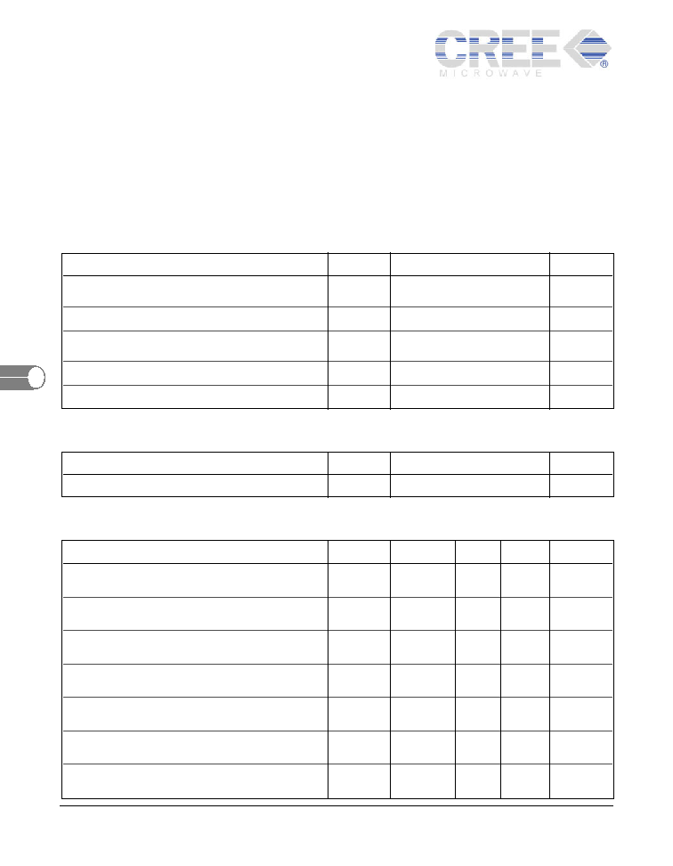
Maximum Ratings
Rating
Symbol
Value
Unit
Drain to Source Voltage, gate
V
DSS
65
Volts
connected to source
Gate to Source Voltage
V
GS
+
/- 20
Volts
Total Device Dissipation @ Tcase = 70∞C
P
D
20
Watts
Derate above 70∞C
0.2
W/∞C
Storage Temperature Range
T
STG
-65 to +150
∞C
Operating Junction Temperature
T
J
200
∞C
Thermal Characteristics
Characteristics
Symbol
Maximum
Unit
Thermal Resistance, Junction to Case
JC
3.6, 3.2
∞C/W
Electrical DC Characteristics
(T
C
=25∞C unless otherwise specified)
Rating
Symbol
Min
Typ
Max
Unit
Drain to Source Voltage, gate connected
BV
DSS
65
-
-
Volts
to source (V
GS
=0, I
DS
=1mA)
Drain to Source Leakage current
I
DSS
-
-
100
µA
(V
DS
=26V, V
GS
=0)
Gate to Source Leakage current
I
GSS
-
-
1.0
µA
(V
GS
=20V, V
DS
=0)
Threshold Voltage
V
TH
2.0
3.0
5.0
Volts
(V
DS
=10V, I
DS
=1mA)
Gate Quiescent Voltage
V
GS
(on)
3.0
4.0
6.0
Volts
(V
DS
=26 V, I
DS
=95mA)
Drain to Source On Voltage
V
DS
(on)
-
0.9
-
Volts
(V
GS
=10V, I
DS
=1A)
Forward Transconductance
G
M
-
0.5
-
S
(V
DS
=10V, I
D
=.5A)

4-3
UPF2010
4
AC Characteristics
(T
C
=25∞C unless otherwise specified)
Rating
Symbol
Min
Typ
Max
Unit
Input Capacitance
C
ISS
-
12.4
-
pF
(V
DS
=26V, V
GS
=0, freq= 1MHz)
Output capacitance
C
OSS
-
8.5
-
pF
(V
DS
= 26V, V
GS
=0V, freq= 1MHz)
Feedback capacitance
C
RSS
-
.6
-
pF
(V
DS
=26V, V
GS
=0V, freq= 1MHz)
RF and Functional Tests
(T
C
=25∞C unless otherwise specified, UltraRF Broadband Fixture)
Rating
Symbol
Min
Typ
Max
Unit
Linear Power Gain, Single Tone
Gplin
12.5
14.5
-
dB
(V
DS
=26V, I
DQ
=95mA, P
OUT
=3W,
f=1840 MHz)
Compressed Power Gain, Single tone
Gps
11.5
13.5
-
dB
(V
DS
=26V, I
DQ
=95mA, P
OUT
=10W,
f=1840 MHz)
Drain Efficiency, Single Tone
40
50
-
%
(V
DS
=26V, I
DQ
=95mA, P
OUT
=10W,
f=1840 MHz)
Intermodulation Distortion, Two Tone
IMD
-
-33
-30
dBc
(V
DS
=26V, I
DQ
=95mA, P
OUT
=10W PEP
f1=1840 MHz, f2=1840.1MHz)
Load Mismatch Tolerance
VSWR
10:1
-
-
(V
DS
=26V, I
DQ
=95mA, P
OUT
=10W,
f=1840 MHz)
CAUTION - MOS Devices are susceptible to damage from ElectroStatic Discharge (ESD). Appropriate
precautions in handling, packaging and testing MOS devices must be observed.
4-4
UPF2010
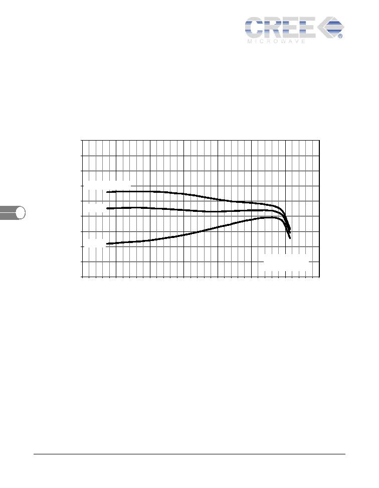
4
10
11
12
13
14
15
16
17
18
19
10
15
20
25
30
35
40
45
V
DD
= 26 V
f = 1960 MHz
Power Gain vs Output Power
G
,
Gain (dB)
PE
P
OUT
, Output Power (dBm)
I
DQ
= 140 mA
50 mA
95 mA

4-5
UPF2010
4