Document Outline
- General Description
- Application
- Table of Contents
- Key Features
- Device Pinout Diagram
- Device Terminal Functions
- Electrical Characteristics
- Device Diagram
- Description of Functional Blocks
- CSR Bluetooth Software Stacks
- External Interfaces
- Schematic
- Package Dimensions
- Ordering Information
- Contact Information
- Document References
- Acronyms and Definitions
- Status of Information
- Record of Changes

BC212015-ds-001f
Production Information
Page 1 of 36
_дм…`зк…
OJbсн…ке~д
Pr
oduct Data Sheet
General Description
Applications
BlueCore2-External is a single chip radio and
baseband IC for Bluetooth 2.4GHz systems.
It is implemented in 0.18
µm CMOS technology.
When used with external flash containing the CSR
Bluetooth software stack, it provides a fully
compliant Bluetooth system for data and voice
communications.
PCs
Cellular Handsets
Cordless Headsets
Personal Digital Assistants (PDAs)
Computer Accessories (Compact flash
Cards, PCMCIA Cards, SD Cards and USB
Dongles)
Mice, Keyboards and Joysticks
Digital Cameras and Camcorders
RAM
DSP
MCU
I/O
2.4 GHz
Radio
XTAL
SPI
UART/USB
PIO
PCM
8Mbit
FLASH
ROM
RF OUT
RF IN
Up to
BlueCore2-External has been designed to reduce
the number of external RF components required,
which ensures module production costs are
minimised.
The device incorporates auto calibration and
built-in self-test routines to simplify development,
type approval and production test. All hardware
and device firmware is fully compliant with the
Bluetooth specification v1.1.
BlueCore2-External Block Diagram
Device Features
Low power 1.8V operation
Small footprint in 96-ball VFBGA
and LGA packages (6x6mm 8x8mm
and 10x10mm)
Fully qualified Bluetooth component
0.18
µm
CMOS technology
Full speed Bluetooth
TM
operation
with full piconet support
Support for 8Mbit external flash
Minimum external components
_дм…`зк…
qj
OJbсн…ке~д=
Single Chip Bluetooth System
Production Information Data Sheet for:
BC212013
(UART only version)
BC212015
(USB and UART version)
March 2003

Table of Contents
BC212015-ds-001f
Production Information
Page 2 of 36
_дм…`зк…
OJbсн…ке~д
Pr
oduct Data Sheet
Table of Contents
1 Key
Features .................................................................................................................................................. 3
2 Device
Pinout Diagram .................................................................................................................................. 4
3 Device
Terminal Functions ........................................................................................................................... 5
4 Electrical
Characteristics .............................................................................................................................. 9
5 Device
Diagram ............................................................................................................................................ 14
6
Description of Functional Blocks ............................................................................................................... 15
6.1 RF Receiver ............................................................................................................................................ 15
6.1.1 Low
Noise Amplifier .................................................................................................................. 15
6.1.2
Analogue to Digital Converter................................................................................................... 15
6.2 RF Transmitter ........................................................................................................................................ 15
6.2.1 IQ
Modulator............................................................................................................................. 15
6.2.2 Power
Amplifier ........................................................................................................................ 15
6.3 RF Synthesiser ....................................................................................................................................... 15
6.4 Baseband and Logic ............................................................................................................................... 15
6.4.1 Memory
Management Unit ....................................................................................................... 15
6.4.2 Burst
Mode Controller............................................................................................................... 15
6.4.3 Physical
Layer
Hardware Engine DSP ..................................................................................... 16
6.4.4 RAM.......................................................................................................................................... 16
6.4.5 External
Memory Driver ............................................................................................................ 16
6.4.6 USB .......................................................................................................................................... 16
6.4.7 Synchronous
Serial Interface.................................................................................................... 16
6.4.8
UART........................................................................................................................................ 16
6.4.9 Audio
PCM Interface................................................................................................................. 16
6.5 Microcontroller ........................................................................................................................................ 17
6.5.1 Programmable I/O .................................................................................................................... 17
7
CSR Bluetooth Software Stacks ................................................................................................................. 18
7.1 BlueCore HCI Stack................................................................................................................................ 18
7.1.1 Key
Features
of the HCI Stack ................................................................................................. 19
7.2 BlueCore RFCOMM Stack...................................................................................................................... 21
7.2.1
Key Features of the BlueCore2-External RFCOMM Stack ....................................................... 21
7.3 BlueCore Virtual Machine Stack ............................................................................................................. 22
7.4 Host-Side Software ................................................................................................................................. 23
7.5 Device Firmware Upgrade ...................................................................................................................... 23
7.6 Additional Software for Other Embedded Applications ........................................................................... 23
7.7 CSR Development Systems.................................................................................................................... 23
8 External
Interfaces....................................................................................................................................... 24
8.1 Transmitter/Receiver Inputs and Outputs ............................................................................................... 24
8.2 Asynchronous Serial Data Port (UART) and USB Port ........................................................................... 24
8.3 PCM CODEC Interface ........................................................................................................................... 24
8.4 Serial Peripheral Interface ...................................................................................................................... 25
8.5 Parallel PIO Port ..................................................................................................................................... 25
8.6 I
2
C Interface ............................................................................................................................................ 25
9 Schematic ..................................................................................................................................................... 26
10 Package
Dimensions ................................................................................................................................... 27
10.1 96-Ball VFBGA....................................................................................................................................... 27
10.2 96-Ball LGA............................................................................................................................................ 28
10.3 96-Ball LFBGA ....................................................................................................................................... 29
11 Ordering
Information ................................................................................................................................... 30
12 Contact Information ..................................................................................................................................... 31
13 Document
References ................................................................................................................................. 32
14 Acronyms and Definitions........................................................................................................................... 33
15 Record
of Changes ...................................................................................................................................... 36

Key Features
BC212015-ds-001f
Production Information
Page 3 of 36
_дм…`зк…
OJbсн…ке~д
Pr
oduct Data Sheet
1 Key
Features
Radio
Operation with common TX/RX terminals
simplifies external matching circuitry and
eliminates external antenna switch
Extensive built-in self-test minimises production
test time
No external trimming is required in production
Full RF reference designs are available
Transmitter
Up to +6dBm RF transmit power with level
control from the on-chip 6-bit DAC over a
dynamic range greater than 30dB
Supports Class 2 and Class 3 radios without the
need for an external power amplifier or TX/RX
switch
Supports Class 1 radios with an external power
amplifier provided by a power control terminal
controlled by an internal 8-bit voltage DAC and
an external RF TX/RX switch
Receiver
Integrated channel filters
Digital demodulator for improved sensitivity and
co-channel rejection
Digitised RSSI available in real time over the
HCI interface
Fast AGC for enhanced dynamic range
Synthesiser
Fully integrated synthesiser; no external VCO
varactor diode or resonator
Compatible with crystals between 8 and 32MHz
(in multiples of 250kHz) or an external clock
Auxiliary Features
Crystal oscillator with built-in digital trimming
Power management includes digital shut down
and wake up commands and an integrated low
power oscillator for ultra-low Park/Sniff/Hold
mode power consumption
Device can be used with an external Master
oscillator and provides a `clock request signal' to
control external clock source
Uncommitted 8-bit ADC and 8-bit DAC are
available to application programs
Baseband and Software
External 8Mbit flash for complete system solution
and application flexibility
32kbyte on-chip RAM allows full speed Bluetooth
data transfer, mixed voice and data, plus full 7
slave piconet operation
Dedicated logic for forward error correction,
header error control, access code correlation,
demodulation, cyclic redundancy check,
encryption bitstream generation, whitening and
transmit pulse shaping
Transcoders for A-law,
µ-law and linear voice
from host and A-law,
µ-law and CVSD voice over
air
Physical Interfaces
Synchronous serial interface up to 4Mbaud
UART interface with programmable Baud rate up
to 1.5MBaud
Full speed USB interface supports OHCI and
UHCI host interfaces. Compliant with USB v1.1
Synchronous bi-directional serial programmable
audio interface
Optional I
2
C
TM
compatible interface
Bluetooth Stack Running on an
Internal Microcontroller
CSR's Bluetooth Protocol Stack runs on-chip in a
variety of configurations:
Standard HCI (UART or USB)
Fully embedded to RFCOMM, thus reducing host
CPU load
Package Options
96-ball LFBGA 10x10x1.4mm 0.80mm pitch
96-ball VFBGA 8x8x1.0mm 0.65mm pitch
96-ball VFBGA 6x6x1.0mm 0.50mm pitch
96-ball VFLGA 6x6x0.65mm 0.50mm pitch
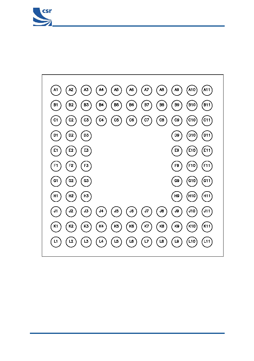
Device Pinout
BC212015-ds-001f
Production Information
Page 4 of 36
_дм…`зк…
OJbсн…ке~д
Pr
oduct Data Sheet
2 Device
Pinout
Diagram
Orientation from top of device
A
B
C
D
E
F
G
H
J
K
L
1
2
3
4
5
6
7
8
9
10
11
Figure 2.1: BlueCore2-External Device Pinout Diagram
Notes:
Device pinout diagram is the same for:
10x10mm LFBGA (BN)
8x8x1mm VFBGA package (DN)
6x6x1mm VFBGA package (EN)
6x6x0.6mm LGA package (LN)

Device Terminal Functions
BC212015-ds-001f
Production Information
Page 5 of 36
_дм…`зк…
OJbсн…ке~д
Pr
oduct Data Sheet
3 Device
Terminal
Functions
Radio Ball
Pad
Type
Description
RF_IN
E1
Analogue
Single ended receiver input
PIO[0]/RXEN C1
Bi-directional with weak
internal pull-up/down
Control output for external LNA (if fitted)
PIO[1]/TXEN C2
Bi-directional with weak
internal pull-up/down
Control output for external PA Class 1
applications only
TX_A
G1
Analogue
Transmitter output/Switched Receiver input
TX_B F1
Analogue
Complement
of
TX_A
AUX_DAC
D2
Analogue
Voltage DAC output
Synthesiser and
Oscillator
Ball Pad
Type
Description
XTAL_IN
L1
Analogue
For crystal or external clock input
XTAL_OUT
L2
Analogue
Drive for crystal
LOOP_FILTER
J1
Analogue
Connection to external PLL loop filter
External Memory
Port
Ball Pad
Type
Description
REB D10
CMOS output, tristatable
with internal weak pull-up
Read enable for external memory (active
low)
WEB E10
CMOS output, tristatable
with internal weak pull-up
Write enable for external memory (active
low)
CSB C10
CMOS output, tristatable
with internal weak pull-up
Chip select for external memory (active low)
Address Lines
Ball
Pad Type
Description
A[0] D9
CMOS output, tristatable
Address line
A[1] E9
CMOS output, tristatable
Address line
A[2] E11
CMOS output, tristatable
Address line
A[3]
F9
CMOS output, tristatable
Address line
A[4]
F10
CMOS output, tristatable
Address line
A[5]
F11
CMOS output, tristatable
Address line
A[6]
G9
CMOS output, tristatable
Address line
A[7]
G10
CMOS output, tristatable Address
line
A[8]
G11
CMOS output, tristatable Address
line
A[9]
H9
CMOS output, tristatable
Address line
A[10]
H10
CMOS output, tristatable
Address line
A[11]
H11
CMOS output, tristatable
Address line
A[12]
J8
CMOS output, tristatable
Address line
A[13]
J9
CMOS output, tristatable
Address line
A[14]
J10
CMOS output, tristatable
Address line
A[15]
J11
CMOS output, tristatable
Address line
A[16]
K9
CMOS output, tristatable
Address line
A[17]
K10
CMOS output, tristatable
Address line
A[18]
K11
CMOS output, tristatable
Address line