 | –≠–ª–µ–∫—Ç—Ä–æ–Ω–Ω—ã–π –∫–æ–º–ø–æ–Ω–µ–Ω—Ç: 636L6C | –°–∫–∞—á–∞—Ç—å:  PDF PDF  ZIP ZIP |
CMOS/TTL CLOCK OSCILLATOR
Document No. 008-0250-0
Page 1 - 4
Rev. C
CTS Communications Components, Inc. 171 Covington Drive Bloomingdale, IL 60108
Phone 630-924-3500
www.ctscorp.com
Toll Free 800-757-6686
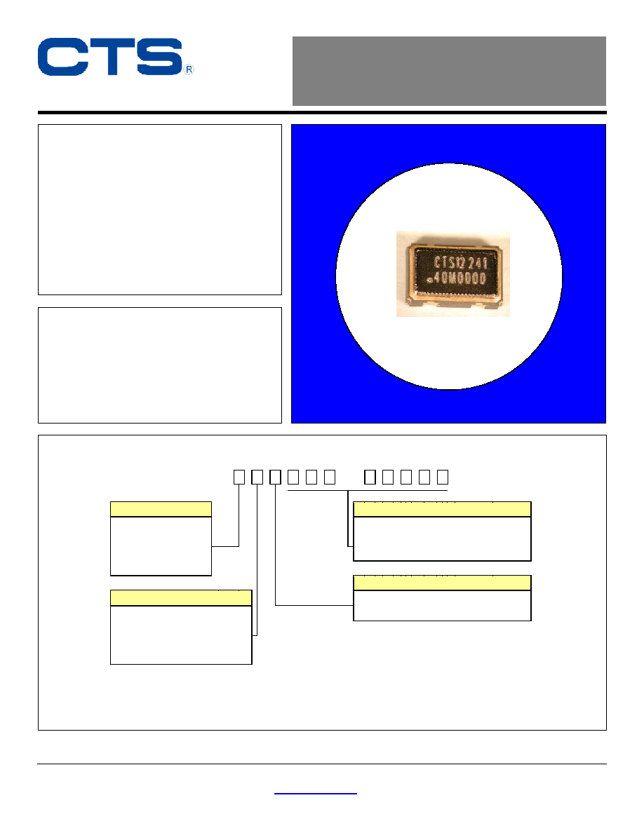
Model 636
Technical
Data
FEATURES
∑ Standard 5x3.2mm Surface Mount Footprint
∑ CMOS/TTL Compatible
∑ Frequency Range 1.0 ≠ 125 MHz
∑ Frequency Stability, ±50 ppm Standard
(±25 ppm and ±20 ppm available)
∑ +1.8Vdc, +2.5Vdc, +3.3Vdc or +5.0Vdc
Operation
∑ Operating Temperature to ≠40∞C to +85∞C
∑ Output Enable Standard
∑ Tape & Reel Packaging
∑ RoHS Compliant
ORDERING INFORMATION
636
M
SUPPLY VOLTAGE
FREQUENCY IN MHz
M - indicates MHz and decimal point.
Frequency is recorded with minimum 5
significant digits to the right of the "M".
M = +1.8V
N = +2.5Vdc
L = +3.3Vdc
S = +5.0Vdc
OPERATING TEMPERATURE RANGE
FREQUENCY STABILITY
C = -20∞C to +70∞C (standard)
I = -40∞C to +85∞C
6 = ± 20 ppm
(-20∞C to +70∞C only)
5 = ± 25 ppm
3 = ± 50 ppm (standard)
2 = ± 100 ppm
(-40∞C to +85∞C only)
Example Part Number: 636L3C032M76800
DESCRIPTION
The Model 636 is a ceramic packaged Clock
oscillator offering reduced size and enhanced
stability. The small size means it is perfect for
any application. The enhanced stability means it
is the perfect choice for today's communications
applications that require tight frequency control.
Document No. 008-0250-0
Page 2 - 4
Rev. C
CTS Communications Components, Inc.
171 Covington Drive
Bloomingdale, IL 60108
630-924-3500
Model 636
5x3.2mm Low Cost
CMOS/TTL Clock Oscillator
ELECTRICAL CHARACTERISTICS
PARAMETER
SYMBOL
CONDITIONS
MIN
TYP
MAX
UNIT
Maximum Supply Voltage
V
CC
- -0.5
-
7.0
V
Storage Temperature
T
STG
- -55
-
125
∞C
Frequency Range
f
O
-
1.0
-
125
MHz
Frequency Stability
(See Note 1 and Ordering Information)
f/f
O
- -
-
20,25,50
or 100
± ppm
Operating Temperature
Commercial
-20 70
Abs
o
l
ut
e M
a
xi
mu
ms
Industrial
T
A
-
-40
25
85
∞C
Supply Voltage
Model 636M
1.62 1.8 1.98
Model 636N
2.25 2.5 2.75
Model 636L
2.97 3.3 3.63
Model 636S
V
CC
± 10 %
4.50 5.0 5.50
V
Supply Current
Model 636M
1.0 MHz to 20 MHz C
L
=15pF
20.1 MHz to 50 MHz C
L
=15pF
50.1 MHz to 125 MHz C
L
=15pF
-
-
-
-
-
-
5
15
20
Model 636N & 636L
1.0 MHz to 20 MHz C
L
=15pF
20.1 MHz to 50 MHz C
L
=15pF
50.1 MHz to 125 MHz C
L
=15pF
-
-
-
-
-
-
7
15
20
Model 636S
I
CC
1.0 MHz to 20 MHz C
L
=15pF
20.1 MHz to 50 MHz C
L
=15pF
50.1 MHz to 125 MHz C
L
=15pF
-
-
-
-
-
-
10
30
40
mA
Output Load
Model 636M
1.0 MHz to 125 MHz
-
-
15
Model 636N & 636L
1.0 MHz to 50 MHz
50.1 MHz to 125 MHz
-
-
-
-
30
15
Model 636S
C
L
1.0 MHz to 50 MHz
50.1 MHz to 80 MHz
80.1 MHz to 125 MHz
-
-
-
-
50
30
15
pF
Output Voltage Levels
Logic '1' Level
V
OH
CMOS
Load
90%V
CC
-
-
Logic '0' Level
V
OL
CMOS
Load
-
- 10%V
CC
V
Output Current
Logic '1' Level (M,N,L,S)
I
OH
V
OH
= 90%V
CC
- -
-0, -4,
-8, -16
Logic '0' Level (M,N,L,S)
I
OL
V
OL
= 10%V
CC
- -
+2, +4,
+8, +16
mA
Output Duty Cycle
SYM
@ 50% Level
45
-
55
%
Rise and Fall Time
@ 10% - 90% Levels
Model 636M, 636N & 636L
1.0 MHz to 20 MHz C
L
=15pF
20.1 MHz to 50 MHz C
L
=15pF
50.1 MHz to 125 MHz C
L
=15pF
-
-
-
8
4
2.5
10
6
3
Model 636S
T
R
, T
F
1.0 MHz to 20 MHz C
L
=15pF
20.1 MHz to 50 MHz C
L
=15pF
50.1 MHz to 125 MHz C
L
=15pF
-
-
-
6
3
1.5
8
5
2
ns
Start Up Time
T
S
Application of V
CC
-
-
10
ms
Enable Function
Enable Input Voltage
Model 636M
Pin 1 Logic '1', Output Enabled
1.26
-
-
Model 636N
Pin 1 Logic '1', Output Enabled
1.75
-
-
Model 636L
Pin 1 Logic '1', Output Enabled
2.0
-
-
Model 636S
V
IH
Pin 1 Logic '1', Output Enabled
4.0
-
-
Disable Input Voltage
Model 636M,N,L
Pin 1 Logic '0', Output Disabled
-
-
0.5
Model 636S
V
IL
Pin 1 Logic '0', Output Disabled
0.8
V
Enable Time (M,N,L,S)
T
PLZ
Pin 1 Logic '1'
- - 10 ms
Elec
tric
al and Wa
ve
for
m
Pa
ram
e
te
rs
Phase Jitter
tjms
Bandwidth 12 KHz - 20 MHz
-
< 1
-
ps RMS
Notes:
1. Inclusive of initial tolerance at time of shipment, changes in supply voltage, load, temperature and first year aging at an average operating temperature
of +40 ∞C.
Document No. 008-0250-0
Page 3 - 4
Rev. C
CTS Communications Components, Inc.
171 Covington Drive
Bloomingdale, IL 60108
630-924-3500
Model 636
5x3.2mm Low Cost
CMOS/TTL Clock Oscillator
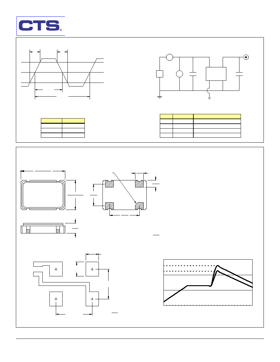
MECHANICAL SPECIFICATIONS
PACKAGE DRAWING
MARKING INFORMATION
1
(1.0)
0.039
PIN 1 IDENTIFIER
4
3
2
Inch
(mm)
Key:
(2.2)
0.087
(1.2)
0.126 ±0.008
(3.2 ±0.2)
0.047
0.197 ±0.008
0.047
0.100
(2.54)
(5.0 ±0.2)
MAX
(1.2)
SUGGESTED SOLDER PAD GEOMETRY
SUGGESTED REFLOW PROFILE
.100 [2.54]
.087 [2.20]
.055 [1.40]
Key:
[mm]
Inch
.047 [1.20]
1
2
3
4
C
BYPASS
C
BYPASS
should be 0.01 uF.
CMOS/TTL OUTPUT WAVEFORM
TEST CIRCUIT, CMOS LOAD
PERIOD (T)
90%, 80%, 2.4V
50%, 1.5V
10%, 20%, 0.5V
DUTY CYCLE = t/T x 100 (%)
V
V
OH
OL
Tr
Tf
UPTIME (t)
POWER
SUPPLY
+
-
+
-
-
+
VM
mA
.01uF
D.U.T.
4
3
1
2
C
L
Including probe
capacitance.
Enable Input
ENABLE TRUTH TABLE
PIN 1
PIN 3
Logic `1'
Output
Open Output
Logic `0'
High Imp.
D.U.T. PIN ASSIGNMENTS
PIN
SYMBOL
DESCRIPTION
1 EOH
Enable
Input
2
GND
Circuit & Package Ground
3 Output
RF
Output
4 V
CC
Supply
Voltage
1. ** - Manufacturing Site Code.
2. YWW ≠ Date code, Y ≠ year, WW ≠ week.
3. XXMXXXX - Frequency marked with 4 significant
digits after the `M'.
0
100
200
300
0
30
60
90
120
150
180
210
240
270
300
Time (Seconds)
Temp.
(∞C)
Maximum 260∞C, 10 seconds
Typical 245∞C
130∞C
CTS ** YWW
32M7680
Document No. 008-0250-0
Page 4 - 4
Rev. C
CTS Communications Components, Inc.
171 Covington Drive
Bloomingdale, IL 60108
630-924-3500
Model 636
5x3.2mm Low Cost
CMOS/TTL Clock Oscillator
QUALITY AND RELIABILITY
Quality systems meet or exceed the requirements of ISO 9000:2000 standards. Reliability audits are performed on
this or similar products with results available upon request.
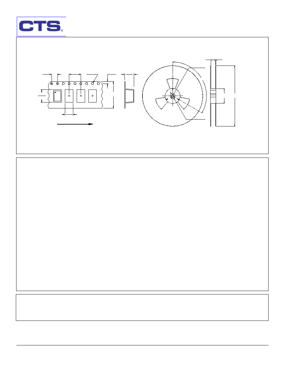
TAPE AND REEL INFORMATION
DIMENSIONS IN MILLIMETERS
DIRECTION OF FEED
3.50
5.20
5.60
3.70
16.0
8.0
4.0
ÿ1.50
1.75
1.30
1.50
ÿ23
ÿ180
ÿ60
ÿ13
120∞
17.5
2.0
Device quantity is 1,000 pieces per 180mm reel.
ENVIRONMENTAL SPECIFICATIONS
Temperature Cycle:
400 cycles from ≠55∞C to +125∞C, 10 minute dwell at each temperature, 1
minute transfer time between temperatures.
Mechanical Shock:
1,500g's, 0.5mS duration, Ω sinewave, 3 shocks each direction along 3
mutually perpendicular planes (18 total shocks).
Sinusoidal Vibration:
0.06 inches double amplitude, 10 to 55 Hz and 20g's, 55 to 2,000 Hz, 3 cycles
each in 3 mutually perpendicular planes (9 times total).
Gross Leak:
No leak shall appear while immersed in an FC40 or equivalent liquid at
+125∞C for 20 seconds.
Fine Leak:
Mass spectrometer leak rates less than 2x10
-8
ATM cc/sec air equivalent.
Resistance to Solder Heat:
Product must survive 3 reflows of +260∞C peak, 10 seconds maximum.
High Temperature Operating Bias:
2,000 hours at +125∞C, maximum bias, disregarding frequency shift.
Frequency Aging:
1,000 hours at +85∞C, full bias, less than ±5 ppm shift.