 | –≠–ª–µ–∫—Ç—Ä–æ–Ω–Ω—ã–π –∫–æ–º–ø–æ–Ω–µ–Ω—Ç: VCT2001A | –°–∫–∞—á–∞—Ç—å:  PDF PDF  ZIP ZIP |

PRELIMINARY
Module Data Sheet: VCT2001A 77.760 MHz
Application: HCMOS Output-Dual Input Clock Generator
Page 1
Rev. "4" 3/28/03
1.0
DESCRIPTION AND APPLICATION
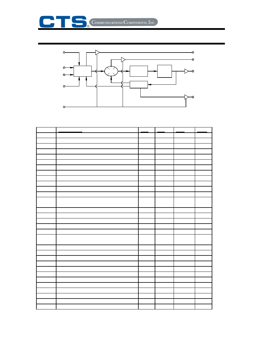
The VCT2001A is a dual reference input 3.3V clock generator module with an
HCMOS output. Reference inputs are selectable by a one-bit select control input.
An alarm output can be used to detect a problem on the selected reference, such as
a loss of lock or a loss of reference. A logic level "1" is indicated from the alarm pin
when there is a problem with the selected reference. The unit operates in the free run
mode when there is a problem with the selected reference, or when free run is invoked by
enabling the forced free run input. Free run accuracy will keep the output to within 20
ppm. The reference will not automatically switch upon loss of reference. Also, all
outputs may be tri-stated for external testing purposes with a signal to the Tri-State/Reset
input.
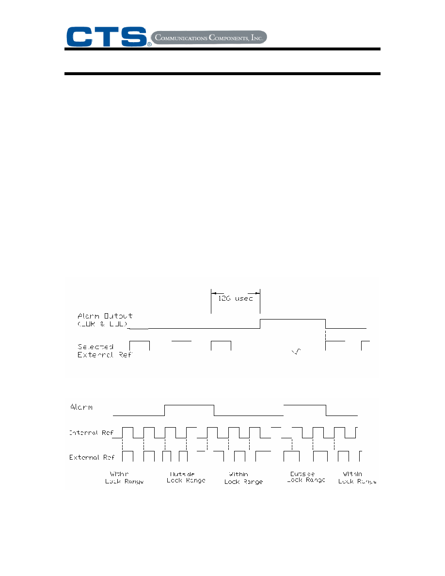
The Loss of Reference alarm detects a missing rising edge within 100 nS of the
missing edge. This is usually around 70 nS.
The 8kHz output is divided from the on-board low jitter oscillator. Output phase
coherence is maintained during reference switching rearrangement, so the output phase
will not necessarily be the same as the reference being used.
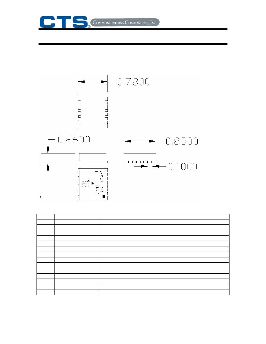
The dimensions of the low jitter module are 0.78" x 0.83" x 0.29" mounted on a
castellated pin FR-4 board.
FEATURES:
∑
Output jitter below 1 ps from 12 kHz to 20 MHz
∑ Two Selectable References @ 8 kHz
∑ Alarm Output Detecting Loss of Reference or Loss of Lock
∑ Tri-Statable Outputs
∑ Force Free Run Function
∑ Automatic Free Run Operation upon loss of both references
∑ Rising Edge Phase Detector allows for any Duty Cycle Reference Input
∑ 3.3 Volt Regulated Power Supply
∑ Small Size: 0.78" x 0.83" x 0.29"
∑ Surface Mount with Castellated Pins
PRELIMINARY
Module Data Sheet: VCT2001A 77.760 MHz
Application: HCMOS Output-Dual Input Clock Generator
Page 2
Rev. "4" 3/28/03
VCT2001A Block Diagram
2.0
ELECTRICAL CHARACTERISTICS
Specification Min Typ Max Units
2.1
Regulated Input Supply Voltage, Vcc
3.10
3.30
3.50
V DC
2.2
Supply Current Drain... @ 3.5V
55
mA
2.3 Frequency
Output
77.760 MHz
2.4 Temperature
Ranges
2.4.1
Operating Temp. Range
0
70
∫C
2.4.2
Storage Temp. Range
-40
85
∫C
2.5 Timing
Parameters
2.5.1 Output Rise and Fall Time (20% 80%)
-
-
3
ns
2.5.2 Input Jitter Tolerance @ 8kHz Reference
(Input Jitter Frequencies > 10 Hz)
2 - - µs
2.5.3 Acquisition Time (Offsetting ref. 20ppm)
-
1
-
s
2.5.4 Jitter Filter Bandwidth
-
-
10
Hz
2.5.5 Capture/pull-in range
-25
-
25
ppm
2.5.6 Free Run Frequency
-20
-
20
ppm
2.5.7 Output Duty Cycle
45
50
55
%
2.5.8 Phase Transient due to Reference switching
(Rearrangement)
50
nS
2.6
Input Logic Levels
2.6.1 ` 0'
-0.5
0.8
V
2.6.2 `1'
2.4
5.5
V
2.7
Output Logic Levels (into 30pF load)
2.7.1 `0'
-0.25
0.8
V
2.7.2 `1'
4.0
Vcc*0.9
V
2.8
Dual Reference input (HCMOS levels)
8
kHz
2.9 Output
load
10 pF
ENABLE / TRISTATE
SEL AB
REF B
REF A
FORCE FREE RUN
8 KHz
ALIGNER
PHASE
DET
ANALOG
FILTER
LOW PASS
f / N
LOW
JITTER
VCXO
FREE RUN STATUS
ALARM
8 KHz
OUTPUT
19.440 MHz
PHASE
OSCILLATOR
OUTPUT
PRELIMINARY
Module Data Sheet: VCT2001A 77.760 MHz
Application: HCMOS Output-Dual Input Clock Generator
Page 3
Rev. "4" 3/28/03
3.0
MECHANICAL CHARACTERISTICS
Pkg. size is 0.780 in (25.40 mm) X 0.830in (26.67 mm) X 0.35 in (8.13 mm) max on an FR4
board with castellated pins.
The module coplanarity is .004 in. (0.101 mm)
Pin Descriptions
Pin #
Pin Name
Description
1
8 kHz Out
Filtered 8 kHz Output
2 N/C
3 N/C
4 GND
Ground
5
F/R
Force Free Run Input("1" is Free Run)
6 Alarm
Alarm Output (1 = Alarm)
7 REF
B
8kHz CMOS Reference Frequency Input
8 REF
A
8kHz CMOS Reference Frequency Input
9 RF
Output
Oscillator Output
10
F/R status
Free Run Status Output (FR = 1)
11
Vcc
Input Voltage-3.3V nominal
12 N/C
13 Reset
Reset / Tri-State (1 = Reset)
14 REFSEL
Reference Select A/B Input (A = 0, B = 1)
PRELIMINARY
Module Data Sheet: VCT2001A 77.760 MHz
Application: HCMOS Output-Dual Input Clock Generator
Page 4
Rev. "4" 3/28/03
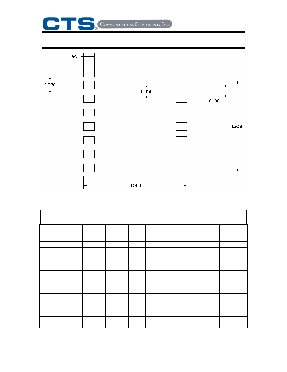
Dimensions for Pads
I/O Truth Table
Inputs
Outputs
Reset/
Tri State
SEL
A/B
REF A
REF B
Free
Run
Free Run
Status
Alarm Oscillator
Output
8 kHz Output
1
X
X
X
X
Tri state
Tri State
Free Run
Tri State
0
X
X
X
1
1
1
Free Run
Free Run
0
0
Ref A
Available
Ref B
Available
0
0
0
Ref A Lock
Ref A Lock
0
1
Not
Available
Ref B
Available
0
0
0
Ref B Lock
Ref B Lock
0
0
Not
Available
Ref B
Available
0
0
0
Free Run
Free Run
0
0 Not
Available
Ref B
Available
0
0
1
Free Run
Free Run
0
1 Ref
A
Available
Not
Available
0
0
1
Free Run
Free Run
0
0 Ref
A
Available
Not
Available
0
0
0
Ref A Lock
Ref A Lock
0
X Not
Available
Not
Available
0
1
1
Free Run
Free Run
PRELIMINARY
Module Data Sheet: VCT2001A 77.760 MHz
Application: HCMOS Output-Dual Input Clock Generator
Page 5
Rev. "4" 3/28/03
4.0
STANDARD ENVIRONMENTAL LIMITS
This product is capable of operating within the following environmental conditions:
4.1 Operating Temperature
0 to +70
∞
C.
4.2 Storage Temperature
-40 to +85
∞
C.
4.3 Humidity (non- Condensing)
95% Relative humidity max @ 40
∞
C.
4.4 Atmospheric Pressure
730 to 780 mm Hg.
4.5 Vibration
10 to 60 Hz with double amplitude of
1.52mm
max.
(1/2 hour in each of 3 perpendicular planes).
4.6 Shock
1/2 sine pulse, 7000G, with pulse width
0.3mSec.
(1 shock in each of 6 directions of 3
perpendicular
planes).
5.0
MAXIMUM SOLDERING PROFILE
Temperature
110
to150
∞
C >183
∞
C
>235
∞
C 240
∞
C
Time
6min
2.5min 0.25min Max
temperature
6.0 ALARM
SITUATIONS
Loss of Reference Situation
Loss of Lock Situation