
Flash Erasable,
Reprogrammable CMOS PAL
Æ
Device
PALCE16V8
Cypress Semiconductor Corporation
∑
3901 North First Street
∑
San Jose
∑
CA 95134
∑
408-943-2600
Document #: 38-03025 Rev. **
Revised September 3, 1998
16V8
Features
∑ Active pull-up on data input pins
∑ Low power version (16V8L)
-- 55 mA max. commercial (10, 15, 25 ns)
-- 65 mA max. industrial (10, 15, 25 ns)
-- 65 mA military (15 and 25 ns)
∑ Standard version has low power
-- 90 mA max. commercial (10, 15, 25 ns)
-- 115 mA max. commercial (7 ns)
-- 130 mA max. military/industrial (10, 15, 25 ns)
∑ CMOS Flash technology for electrical erasability and
reprogrammability
∑ PCI compliant
∑ User-programmable macrocell
-- Output polarity control
-- Individually selectable for registered or combinato-
rial operation
∑ Up to 16 input terms and 8 outputs
∑ 7.5 ns com'l version
5 ns t
CO
5 ns t
S
7.5 ns t
PD
125-MHz state machine
∑ 10 ns military/industrial versions
7 ns t
CO
10 ns t
S
10 ns t
PD
62-MHz state machine
∑ High reliability
-- Proven Flash technology
-- 100% programming and functional testing
Functional Description
The Cypress PALCE16V8 is a CMOS Flash Electrical Eras-
able second-generation programmable array logic device. It is
implemented with the familiar sum-of-product (AND-OR) logic
structure and the programmable macrocell.
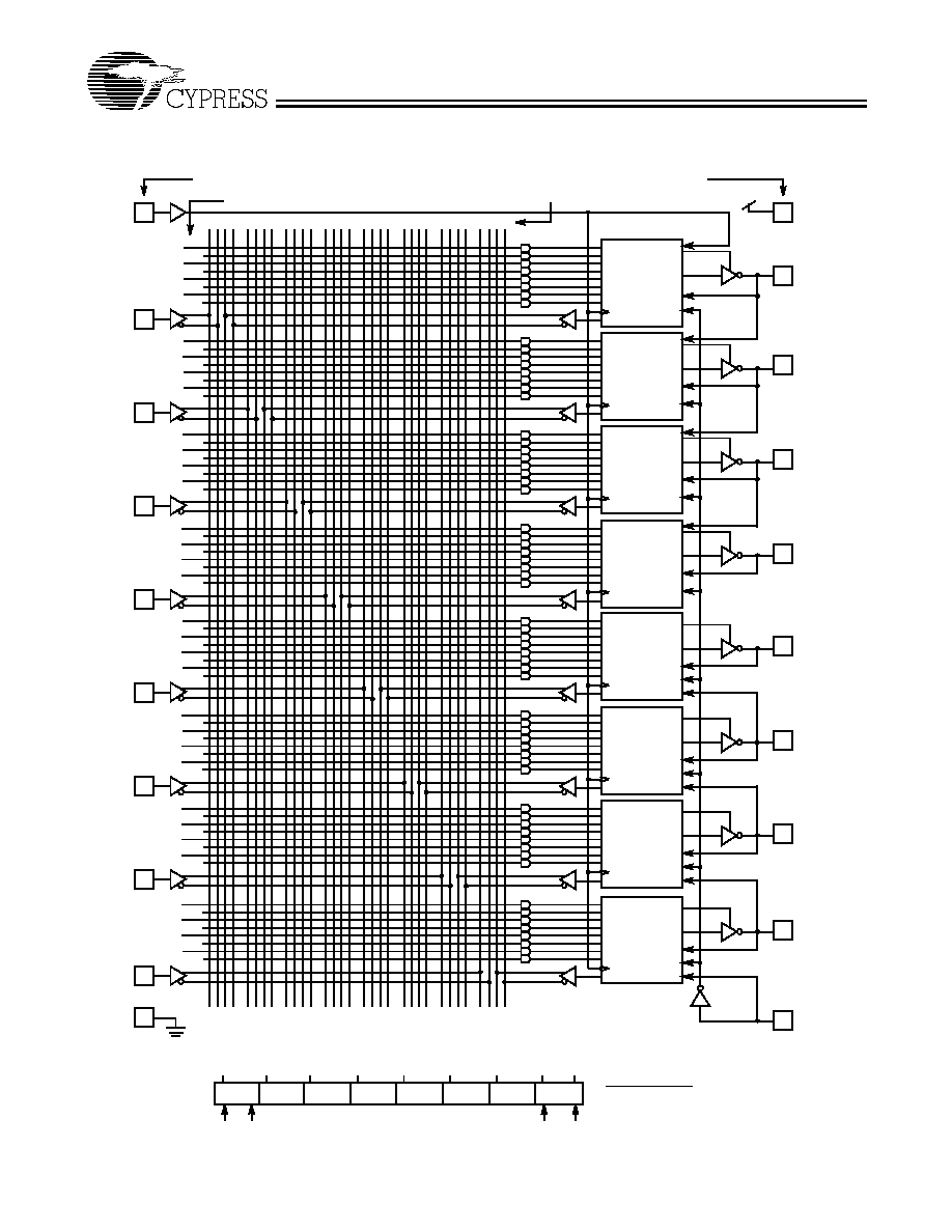
16V8≠1
8
8
8
8
8
8
8
8
10
9
8
7
6
5
4
3
2
1
11
12
13
14
15
16
17
18
19
20
PROGRAMMABLE
AND ARRAY
(64 x 32)
Macrocell
Macrocell
Macrocell
Macrocell
Macrocell
Macrocell
Macrocell
Macrocell
GND
I
8
I
7
I
6
I
5
I
4
I
3
I
2
I
1
CLK/I
0
OE/I
9
I/O
0
I/O
1
I/O
2
I/O
3
I/O
4
I/O
5
I/O
6
I/O
7
V
CC
Logic Block Diagram (PDIP/CDIP)
Pin Configurations
PLCC/LCC
Top View
16V8≠2
16V8≠3
18
17
16
15
14
4
5
6
7
8
9 10111213
3 2 1
19
I
I
CLK
/
I
I/
O
20
V
CC
OE
/I
I/
O
I/
O
CLK/I
0
I
1
I
2
I
3
I
4
I
8
GND
OE/I
9
V
CC
I/O
7
I/O
6
I/O
4
I/O
3
I/O
2
I/O
0
I/O
5
I
5
I
6
I
7
I/O
1
1
2
3
4
5
6
7
8
9
10
11
12
16
15
14
13
17
20
19
18
DIP
I
3
I
4
I
5
I
6
I
7
2
1
0
7
I/O
6
I/O
4
I/O
3
I/O
2
I/O
5
8
I
GND
9
0
1
Top View
PALCE16V8
Document #: 38-03025 Rev. **
Page 2 of 13
Functional Description
(continued)
The PALCE16V8 is executed in a 20-pin 300-mil molded DIP,
a 300-mil cerdip, a 20-lead square ceramic leadless chip car-
rier, and a 20-lead square plastic leaded chip carrier.
The device provides up to 16 inputs and 8 outputs. The
PALCE16V8 can be electrically erased and reprogrammed.
The programmable macrocell enables the device to function
as a superset to the familiar 20-pin PLDs such as 16L8, 16R8,
16R6, and 16R4.
The PALCE16V8 features 8 product terms per output and 32
input terms into the AND array. The first product term in a mac-
rocell can be used either as an internal output enable control
or as a data product term.
There are a total of 18 architecture bits in the PALCE16V8
macrocell; two are global bits that apply to all macrocells and
16 that apply locally, two bits per macrocell. The architecture
bits determine whether the macrocell functions as a register or
combinatorial with inverting or noninverting output. The output
enable control can come from an external pin or internally from
a product term. The output can also be permanently enabled,
functioning as a dedicated output or permanently disabled,
functioning as a dedicated input. Feedback paths are select-
able from either the input/output pin associated with the mac-
rocell, the input/output pin associated with an adjacent pin, or
from the macrocell register itself.
Power-Up Reset
All registers in the PALCE16V8 power-up to a logic LOW for
predictable system initialization. For each register, the associ-
ated output pin will be HIGH due to active-LOW outputs.
Electronic Signature
An electronic signature word is provided in the PALCE16V8
that consists of 64 bits of programmable memory that can con-
tain user-defined data.
Security Bit
A security bit is provided that defeats the readback of the in-
ternal programmed pattern when the bit is programmed.
Low Power
The Cypress PALCE16V8 provides low-power operation
through the use of CMOS technology, and increased testability
with Flash reprogrammability.
Product Term Disable
Product Term Disable (PTD) fuses are included for each prod-
uct term. The PTD fuses allow each product term to be individ-
ually disabled.
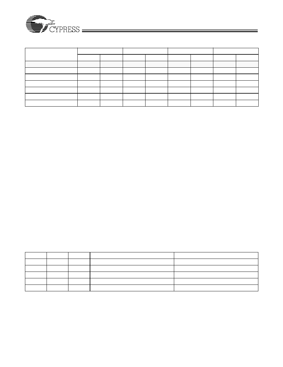
Selection Guide
Generic Part Number
t
PD
ns
t
S
ns
t
CO
ns
I
CC
mA
Com'l/Ind
Mil
Com'l/Ind
Mil
Com'l/Ind
Mil
Com'l
Mil/Ind
PALCE16V8-5
5
3
4
115
PALCE16V8-7
7.5
7
5
115
PALCE16V8-10
10
10
10
10
7
10
90
130
PALCE16V8-15
15
15
12
12
10
10
90
130
PALCE16V8-25
25
25
15
20
12
12
90
130
PALCE16V8L-15
15
15
12
12
10
12
55
65
PALCE16V8L-25
25
25
15
20
12
20
55
65
Shaded area contains preliminary information.
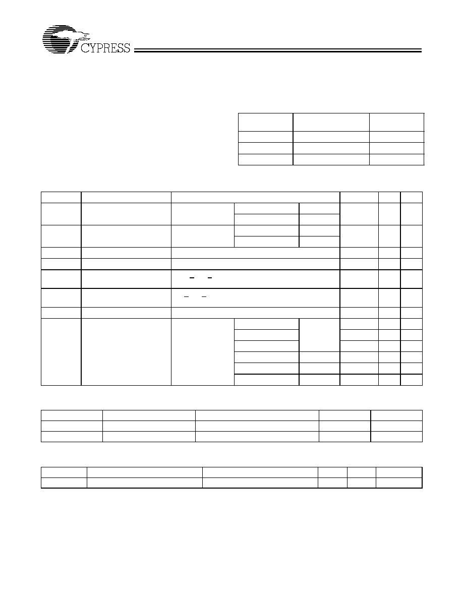
Configuration Table
CG
0
CG
1
CL0
x
Cell Configuration
Devices Emulated
0
1
0
Registered Output
Registered Med PALs
0
1
1
Combinatorial I/O
Registered Med PALs
1
0
0
Combinatorial Output
Small PALs
1
0
1
Input
Small PALs
1
1
1
Combinatorial I/O
16L8 only

PALCE16V8
Document #: 38-03025 Rev. **
Page 3 of 13
Macrocell
Q
Q
D
CLK
16V8≠4
1
1
0
0
1
X
CL1
x
0
1
X
0
1 1
I/O
x
From
Adjacent
Pin
CL0
x
CG
1
for pin 13 to 18
CG
0
for pin 12 and 19
1
0
0
1
1 1
0 0
0
1
X
0
1 1
OE
V
CC
To
Adjacent
Macrocell
CL0
x
CG
1
V
CC
PALCE16V8
Document #: 38-03025 Rev. **
Page 4 of 13
Maximum Ratings
(Above which the useful life may be impaired. For user guide-
lines, not tested.)
Storage Temperature ................................. ≠65
∞
C to +150
∞
C
Ambient Temperature with
Power Applied............................................. ≠55
∞
C to +125
∞
C
Supply Voltage to Ground Potential
(Pin 24 to Pin 12) ........................................... ≠0.5V to +7.0V
DC Voltage Applied to Outputs
in High Z State ............................................... ≠0.5V to +7.0V
DC Input Voltage............................................ ≠0.5V to +7.0V
Output Current into Outputs (LOW)............................. 24 mA
DC Programming Voltage............................................. 12.5V
Latch-Up Current ..................................................... >200 mA
Operating Range
Range
Ambient
Temperature
V
CC
Commercial
0
∞
C to +75
∞
C
5V
±
5%
Military
[1]
≠55
∞
C to +125
∞
C
5V
±
10%
Industrial
≠40
∞
C to +85
∞
C
5V
±
10%
Electrical Characteristics
Over the Operating Range
[2]
Parameter
Description
Test Conditions
Min.
Max.
Unit
V
OH
Output HIGH Voltage
V
CC
= Min.,
V
IN
= V
IH
or V
IL
I
OH
= ≠3.2 mA
Com'l
2.4
V
I
OH
= ≠2 mA
Mil/Ind
V
OL
Output LOW Voltage
V
CC
= Min.,
V
IN
= V
IH
or V
IL
I
OL
= 24 mA
Com'l
0.5
V
I
OL
= 12 mA
Mil/Ind
V
IH
Input HIGH Level
Guaranteed Input Logical HIGH Voltage for All Inputs
[3]
2.0
V
V
IL
[4]
Input LOW Level
Guaranteed Input Logical LOW Voltage for All Inputs
[3]
≠0.5
0.8
V
I
IH
Input or I/O HIGH Leakage
Current
3.5V < V
IN
< V
CC
10
µ
A
I
IL
[5]
Input or I/O LOW Leakage
Current
0V < V
IN
< V
IN
(Max.)
≠100
µ
A
I
SC
Output Short Circuit Current V
CC
= Max., V
OUT
= 0.5V
[6, 7]
≠30
≠150
mA
I
CC
Operating Power Supply
Current
V
CC
= Max.,
V
IL
= 0V, V
IH
= 3V,
Output Open,
f = 15 MHz
(counter)
5, 7 ns
Com'l
115
mA
10, 15, 25 ns
90
mA
15L, 25L ns
55
mA
10, 15, 25 ns
Mil/Ind
130
mA
15L, 25L ns
Mil.
65
mA
15L, 25L ns
Ind.
65
mA
Capacitance
[7]
Parameter
Description
Test Conditions
Typ.
Unit
C
IN
Input Capacitance
V
IN
= 2.0V @ f = 1 MHz
5
pF
C
OUT
Output Capacitance
V
OUT
= 2.0V @ f = 1 MHz
5
pF
Endurance Characteristics
[7]
Parameter
Description
Test Conditions
Min.
Max.
Unit
N
Minimum Reprogramming Cycles
Normal Programming Conditions
100
Cycles
Notes:
1.
T
A
is the "instant on" case temperature.
2.
See the last page of this specification for Group A subgroup testing information.
3.
These are absolute values with respect to device ground. All overshoots due to system or tester noise are included.
4.
V
IL
(Min.) is equal to ≠3.0V for pulse durations less than 20 ns.
5.
The leakage current is due to the internal pull-up resistor on all pins.
6.
Not more than one output should be tested at a time. Duration of the short circuit should not be more than one second. V
OUT
= 0.5V has been chosen to avoid test problems
caused by tester ground degradation.
7.
Tested initially and after any design or process changes that may affect these parameters.
PALCE16V8
Document #: 38-03025 Rev. **
Page 5 of 13
AC Test Loads and Waveforms
90%
10%
3.0V
GND
90%
10%
ALL INPUT PULSES
< 2 ns
< 2 ns
16V8≠5
OUTPUT
R2
R1
C
L
S1
5V
TEST POINT
16V8≠6
Commercial
Military
Specification
S
1
C
L
R
1
R
2
R
1
R
2
Measured Output Value
t
PD
, t
CO
Closed
50 pF
200
390
390
750
1.5V
t
PZX
, t
EA
Z
∑
H: Open
Z
∑
L: Closed
1.5V
t
PXZ
, t
ER
H
∑
Z: Open
L
∑
Z: Closed
5 pF
H
∑
Z: V
OH
≠ 0.5V
L
∑
Z: V
OL
+ 0.5V
PALCE16V8
Document #: 38-03025 Rev. **
Page 6 of 13
Commercial and Industrial Switching Characteristic
s
[
2]
16V8-5
16V8-7
16V8-10
16V8-15
16V8-25
Parameter
Description
Min.
Max.
Min.
Max.
Min.
Max.
Min.
Max.
Min.
Max.
Unit
t
PD
Input to Output
Propagation
Delay
[8, 9]
1
5
3
7.5
3
10
3
15
3
25
ns
t
PZX
OE to Output
Enable
1
6
6
10
15
20
ns
t
PXZ
OE to Output
Disable
1
5
6
10
15
20
ns
t
EA
Input to Output
Enable Delay
[7]
1
6
9
10
15
25
ns
t
ER
Input to Output
Disable Delay
[7, 10]
1
5
9
10
15
25
ns
t
CO
Clock to Output
Delay
[8,9]
1
4
2
5
2
7
2
10
2
12
ns
t
S
Input or Feedback
Set-Up Time
3
5
7.5
12
15
ns
t
H
Input Hold Time
0
0
0
0
0
ns
t
P
External Clock
Period (t
CO
+ t
S
)
7
10
14.5
22
27
ns
t
WH
Clock Width HIGH
[7]
3
4
6
8
12
ns
t
WL
Clock Width LOW
[7]
3
4
6
8
12
ns
f
MAX1
External Maximum
Frequency
(1/(t
CO
+ t
S
))
[7, 11]
143
100
69
45.5
37
MHz
f
MAX2
Data Path Maximum Fre-
quency (1/(t
WH
+ t
WL
))
[7, 12]
166
125
83
62.5
41.6
MHz
f
MAX3
Internal Feedback
Maximum Frequency
(1/(t
CF
+ t
S
))
[7, 13]
166
125
74
50
40
MHz
t
CF
Register Clock to
Feedback Input
[7, 14]
3
3
6
8
10
ns
t
PR
Power-Up Reset Time
[7]
1
1
1
1
1
µ
s
Shaded area contains preliminary information.
Notes:
8.
Min. times are tested initially and after any design or process changes that may affect these parameters.
9.
This specification is guaranteed for all device outputs changing state in a given access cycle.
10. This parameter is measured as the time after OE pin or internal disable input disables or enables the output pin. This delay is measured to the point at which a previous
HIGH level has fallen to 0.5 volts below V
OH
min. or a previous LOW level has risen to 0.5 volts above V
OL
max.
11.
This specification indicates the guaranteed maximum frequency at which a state machine configuration with external feedback can operate.
12. This specification indicates the guaranteed maximum frequency at which the device can operate in data path mode.
13. This specification indicates the guaranteed maximum frequency at which a state machine configuration with internal only feedback can operate.
14. This parameter is calculated from the clock period at f
MAX
internal (1/f
MAX3
) as measured (see Note 7 above) minus t
S
.
PALCE16V8
Document #: 38-03025 Rev. **
Page 7 of 13
Military Switching Characteristics
[
7]
16V8-10
16V8-15
16V8-25
Parameter
Description
Min.
Max.
Min.
Max.
Min.
Max.
Unit
t
PD
Input to Output
Propagation Delay
[8, 9]
3
10
3
15
3
25
ns
t
PZX
OE to Output Enable
10
15
20
ns
t
PXZ
OE to Output Disable
10
15
20
ns
t
EA
Input to Output Enable Delay
[7]
10
15
25
ns
t
ER
Input to Output Disable Delay
[7, 10]
10
15
25
ns
t
CO
Clock to Output Delay
[8, 9]
2
7
2
10
2
12
ns
t
S
Input or Feedback Set-Up Time
10
12
15
ns
t
H
Input Hold Time
.5
.5
.5
ns
t
P
External Clock Period (t
CO
+ t
S
)
17
22
27
ns
t
WH
Clock Width HIGH
[7]
6
8
12
ns
t
WL
Clock Width LOW
[7]
6
8
12
ns
f
MAX1
External Maximum Frequency
(1/(t
CO
+ t
S
)
[7, 11]
58
45.5
37
MHz
f
MAX2
Data Path Maximum Frequency
(1/(t
WH
+ t
WL
))
[7, 12]
83
62.5
41.6
MHz
f
MAX3
Internal Feedback Maximum
Frequency (1/(t
CF
+ t
S
))
[7, 13]
62.5
50
40
MHz
t
CF
Register Clock to
Feedback Input
[7, 14]
6
8
10
ns
t
PR
Power-Up Reset Time
[7]
1
1
1
µ
s
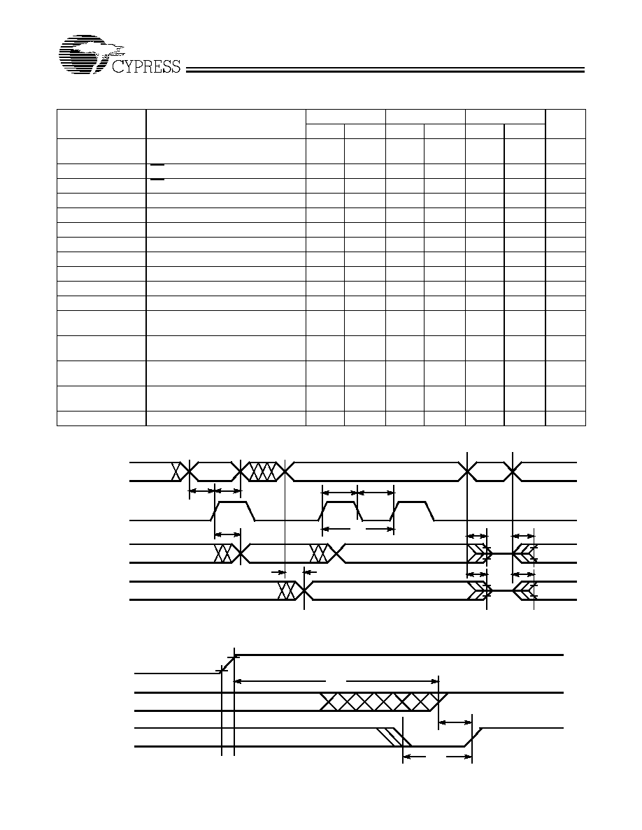
Switching Waveform
t
S
t
H
t
WL
t
WH
t
P
t
CO
t
PD
16V8≠7
t
PXZ
, t
ER
INPUTS, I/O,
REGISTERED
FEEDBACK
CP
REGISTERED
OUTPUTS
COMBINATORIAL
OUTPUTS
t
PXZ
, t
ER
t
EA
, t
PZX
t
EA
, t
PZX
[10]
[10]
[10]
[10]
Power-Up Reset Waveform
t
PR
POWER
CLOCK
t
S
t
WL
10%
REGISTERED
ACTIVE LOW
OUTPUTS
16V8≠8
SUPPLY VOLTAGE
t
PR
MAX = 1
µ
s
90%
V
CC
PALCE16V8
Document #: 38-03025 Rev. **
Page 8 of 13
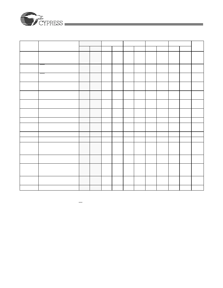
Functional Logic Diagram for PALCE16V8
0
1
16
20
24
28
00
12
8
4
31
19
23
27
15
11
7
3
2
19
0
16
20
24
28
12
8
4
31
19
23
27
15
11
7
3
11
16V8≠9
MC7
CL1=2048
CL0=2120
PTD=2128
-2135
3
18
MC6
CL1=2049
CL0=2121
PTD=2136
-2143
4
17
MC5
CL1=2050
CL0=2122
PTD=2144
-2151
5
16
MC4
CL1=2051
CL0=2123
PTD=2152
-2159
6
15
MC3
CL1=2052
CL0=2124
PTD=2160
-2167
7
14
MC2
CL1=2053
CL0=2125
PTD=2168
-2175
8
13
MC1
CL1=2054
CL0=2126
PTD=2176
-2183
9
12
MC0
CL1=2055
CL0=2127
PTD=2184
-2191
10
USER
ELECTRONIC SIGNATURE ROW
BYTE 0
BYTE 1
BYTE 2
BYTE 3
BYTE 4
BYTE 5
BYTE 6
BYTE 7
2056
2064
2072
2080
2088
2096
2104
2112
2119
MSB
MSB
LSB
LSB
CG
0
=2192
CG
1
=2193
20
V
CC
PRODUCT LINE FIRST CELL NUMBERS
PIN NUMBERS
INPUT LINE
NUMBERS
PIN NUMBERS
32
96
160
224
64
128
192
256
288
352
416
480
320
384
448
512
544
608
672
736
576
640
704
768
800
864
928
992
832
896
960
1024
1056
1120
1184
1248
1088
1152
1216
1280
1312
1376
1440
1504
1344
1408
1472
1536
1568
1632
1696
1760
1600
1664
1728
1792
1824
1888
1952
2016
1856
1920
1984
GLOBAL ARCH BITS
PALCE16V8
Document #: 38-03025 Rev. **
Page 9 of 13
Ordering Information
I
CC
(mA)
t
PD
(ns)
t
S
(ns)
t
CO
(ns)
Ordering Code
Pack-
age
Name
Package Type
Operating
Range
115
5
3
4
PALCE16V8-5JC
J61
20-Lead Plastic Leaded Chip Carrier
Commercial
115
7.5
5
5
PALCE16V8-7JC
J61
20-Lead Plastic Leaded Chip Carrier
Commercial
PALCE16V8-7PC
P5
20-Lead (300-Mil) Molded DIP
90
10
7.5
7
PALCE16V8-10JC
J61
20-Lead Plastic Leaded Chip Carrier
PALCE16V8-10PC
P5
20-Lead (300-Mil) Molded DIP
130
10
7.5
7
PALCE16V8-10JI
J61
20-Lead Plastic Leaded Chip Carrier
Industrial
PALCE16V8-10PI
P5
20-Lead (300-Mil) Molded DIP
130
10
10
7
PALCE16V8-10DMB
D6
20-Lead (300-Mil) CerDIP
Military
PALCE16V8-10LMB
L61
20-Pin Square Leadless Chip Carrier
90
15
12
10
PALCE16V8-15JC
J61
20-Lead Plastic Leaded Chip Carrier
Commercial
PALCE16V8-15PC
P5
20-Lead (300-Mil) Molded DIP
130
15
12
10
PALCE16V8-15PI
P5
20-Lead(300Mil) Molded DIP
Industrial
PALCE16V8-15DMB
D6
20-Lead (300-Mil) CerDIP
Military
PALCE16V8-15LMB
L61
20-Pin Square Leadless Chip Carrier
90
25
15
12
PALCE16V8-25JC
J61
20-Lead Plastic Leaded Chip Carrier
Commercial
PALCE16V8-25PC
P5
20-Lead (300-Mil) Molded DIP
130
25
15
12
PALCE16V8-25JI
J61
20-Lead Plastic Leaded Chip Carrier
Industrial
PALCE16V8-25DMB
D6
20-Lead (300-Mil) CerDIP
Military
PALCE16V8-25LMB
L61
20-Pin Square Leadless Chip Carrier
55
10
7.5
7
PALCE16V8L-10JC
J61
20-Lead Plastic Leaded Chip Carrier
Commercial
PALCE16V8L-10PC
P5
20-Lead (300-Mil) Molded DIP
65
10
10
7
PALCE16V8L-10JI
J61
20-Lead Plastic Leaded Chip Carrier
Industrial
PALCE16V8L-10PI
P5
20-Lead (300-Mil) Molded DIP
55
15
12
10
PALCE16V8L-15JC
J61
20-Lead Plastic Leaded Chip Carrier
Commercial
PALCE16V8L-15PC
P5
20-Lead (300-Mil) Molded DIP
65
15
12
10
PALCE16V8L-15DMB
D6
20-Lead (300-Mil) CerDIP
Military
PALCE16V8L-15LMB
L61
20-Pin Square Leadless Chip Carrier
55
25
15
12
PALCE16V8L-25JC
J61
20-Lead Plastic Leaded Chip Carrier
Commercial
PALCE16V8L-25PC
P5
20-Lead (300-Mil) Molded DIP
Military
65
25
15
12
PALCE16V8L-25DMB
D6
20-Lead (300-Mil) CerDIP
PALCE16V8L-25LMB
L61
20-Pin Square Leadless Chip Carrier
Shaded area contains preliminary information.
PALCE16V8
Document #: 38-03025 Rev. **
Page 10 of 13
MILITARY SPECIFICATIONS
Group A Subgroup Testing
DC Characteristics
Parameter
Subgroups
V
OH
1, 2, 3
V
OL
1, 2, 3
V
IH
1, 2, 3
V
IL
1, 2, 3
I
IX
1, 2, 3
I
OZ
1, 2, 3
I
CC
1, 2, 3
Switching Characteristics
Parameter
Subgroups
t
PD
9, 10, 11
t
CO
9, 10, 11
t
S
9, 10, 11
t
H
9, 10, 11
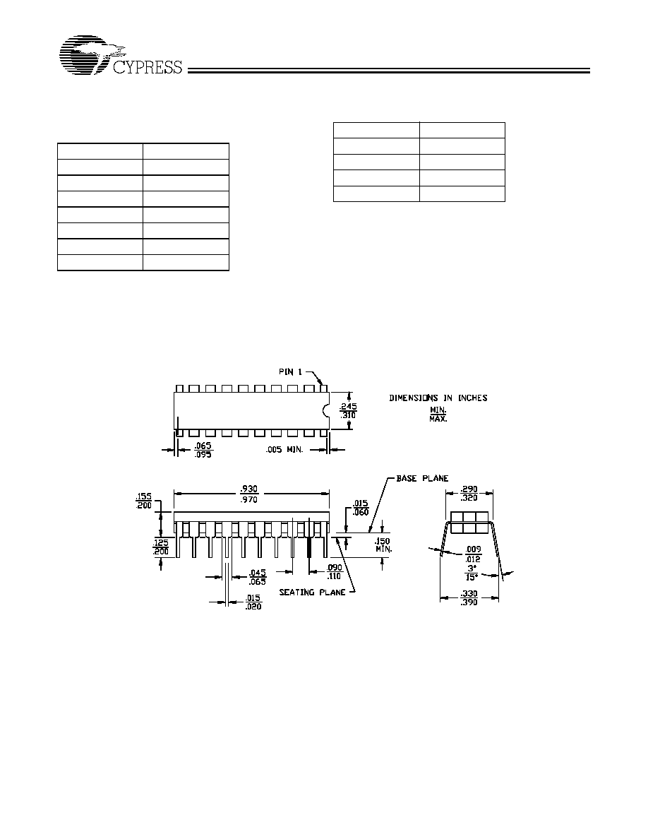
Package Diagrams
20-Lead (300-Mil) CerDIP D6
MIL-STD-1835 D-8 Config. A
51-80029

PALCE16V8
Document #: 38-03025 Rev. **
Page 11 of 13
Package Diagrams
(continued)
20-Lead Plastic Leaded Chip Carrier J61
51-85000-A
20-Square Leadless Chip Carrier L61
51-80049
PALCE16V8
Document #: 38-03025 Rev. **
Page 12 of 13
© Cypress Semiconductor Corporation, 1998. The information contained herein is subject to change without notice. Cypress Semiconductor Corporation assumes no responsibility for the use
of any circuitry other than circuitry embodied in a Cypress Semiconductor product. Nor does it convey or imply any license under patent or other rights. Cypress Semiconductor does not authorize
its products for use as critical components in life-support systems where a malfunction or failure may reasonably be expected to result in significant injury to the user. The inclusion of Cypress
Semiconductor products in life-support systems application implies that the manufacturer assumes all risk of such use and in doing so indemnifies Cypress Semiconductor against all charges.
Package Diagrams
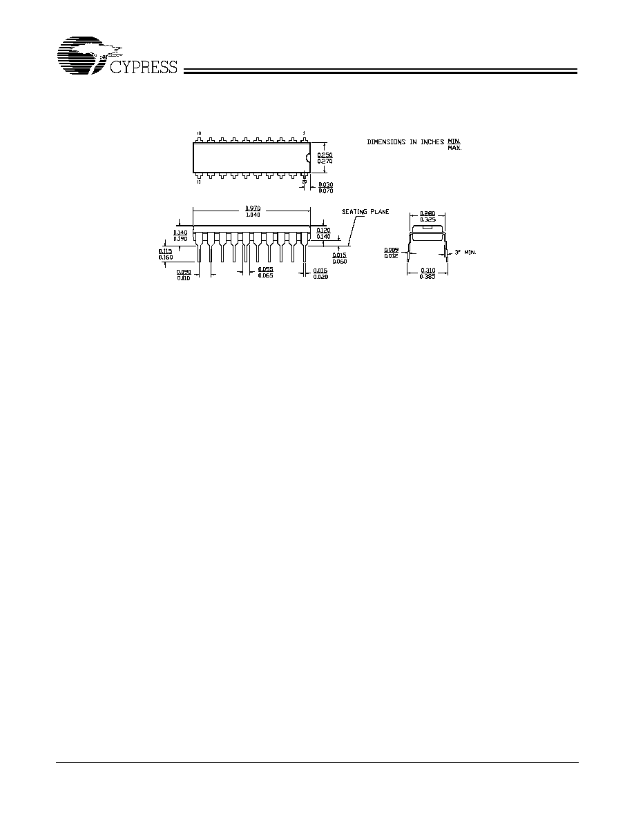
(continued)
51-85011-A
20-Lead (300-Mil) Molded DIP P5

PALCE16V8
Document #: 38-03025 Rev. **
Page 13 of 13
Document Title: PALCE16V8 Flash Erasable, Reprogrammable CMOS PALÆ Device
Document Number: 38-03025
REV.
ECN NO.
Issue
Date
Orig. of
Change
Description of Change
**
106370
07/11/01
SZV
Change from Spec Number: 38-00364 to 38-03025