 | –≠–ª–µ–∫—Ç—Ä–æ–Ω–Ω—ã–π –∫–æ–º–ø–æ–Ω–µ–Ω—Ç: 7C142-35 | –°–∫–∞—á–∞—Ç—å:  PDF PDF  ZIP ZIP |

2Kx8 Dual-Port Static RAM
fax id: 5201
CY7C132/CY7C136
CY7C142/CY7C146
Cypress Semiconductor Corporation
∑
3901 North First Street
∑
San Jose
∑
CA 95134
∑
408-943-2600
December 1989 ≠ Revised March 27, 1997
1CY 7C13 2/ CY7C1 36
Features
∑ True Dual-Ported memory cells which allow simulta-
neous reads of the same memory location
∑ 2K x 8 organization
∑ 0.65-micron CMOS for optimum speed/power
∑ High-speed access: 15 ns
∑ Low operating power: I
CC
= 90 mA (max.)
∑ Fully asynchronous operation
∑ Automatic power-down
∑ Master CY7C132/CY7C136 easily expands data bus
width to 16 or more bits using slave CY7C142/CY7C146
∑ BUSY output flag on CY7C132/CY7C136; BUSY input
on CY7C142/CY7C146
∑ INT flag for port-to-port communication (52-pin
PLCC/PQFP versions)
∑ Available in 48-pin DIP (CY7C132/142), 52-pin PLCC and
52-pin TQFP (CY7C136/146)
∑ Pin-compatible and functionally equivalent to
IDT7132/IDT7142
Functional Description
The CY7C132/CY7C136/CY7C142 and CY7C146 are
high-speed CMOS 2K by 8 dual-port static RAMs. Two ports
are provided to permit independent access to any location in
memory. The CY7C132/ CY7C136 can be utilized as either a
standalone 8-bit dual-port static RAM or as a MASTER du-
al-port RAM in conjunction with the CY7C142/CY7C146
SLAVE dual-port device in systems requiring 16-bit or greater
word widths. It is the solution to applications requiring shared
or buffered data such as cache memory for DSP, bit-slice, or
multiprocessor designs.
Each port has independent control pins; chip enable (CE),
write enable (R/W), and output enable (OE). BUSY flags are
provided on each port. In addition, an interrupt flag (INT) is
provided on each port of the 52-pin PLCC version. BUSY sig-
nals that the port is trying to access the same location currently
being accessed by the other port. On the PLCC version, INT
is an interrupt flag indicating that data has been placed in a
unique location (7FF for the left port and 7FE for the right port).
An automatic power-down feature is controlled independently
on each port by the chip enable (CE) pins.
The CY7C132/CY7C142 are available in 48-pin DIP. The
CY7C136/CY7C146 are available in 52-pin PLCC and PQFP.
Notes:
1.
CY7C132/CY7C136 (Master): BUSY is open drain output and requires pull-up resistor.
CY7C142/CY7C146 (Slave): BUSY is input.
2.
Open drain outputs; pull-up resistor required.
Logic Block Diagram
Pin Configuration
C132-1
C132-2
13
14
15
16
17
18
19
20
21
22
23
26
27
28
32
31
30
29
33
36
35
34
24
25
GND
R/W
L
BUSY
L
[1]
CE
L
OE
L
A
10L
A
0L
A
0R
A
10R
R/W
R
CE
R
OE
R
CE
R
OE
R
CE
L
OE
L
R/W
L
R/W
R
I/O
7L
I/O
0L
I/O
7R
I/O
0R
BUSY
R
[1]
INT
L
[2]
INT
R
[2]
ARBITRATION
LOGIC
(7C132/7C136 ONLY)
AND
INTERRUPTLOGIC
(7C136/7C146 ONLY)
CONTROL
I/O
CONTROL
I/O
MEMORY
ARRAY
ADDRESS
DECODER
ADDRESS
DECODER
1
2
3
4
5
6
7
8
9
10
11
38
39
40
44
43
42
41
45
48
47
46
12
37
R/W
L
CE
L
BUSY
L
A
10L
OE
L
A
0L
A
1L
A
2L
A
3L
A
4L
A
5L
A
6L
A
7L
A
8L
A
9L
I/O
0L
I/O
1L
I/O
2L
I/O
3L
I/O
4L
I/O
5L
I/O
6L
I/O
7L
CE
R
R/W
R
BUSY
R
A
10R
OE
R
A
0R
A
1R
A
2R
A
3R
A
4R
A
5R
A
6R
A
7R
A
8R
A
9R
I/O
7R
I/O
6R
I/O
5R
I/O
4R
I/O
3R
I/O
2R
I/O
1R
I/O
0R
V
CC
DIP
Top View
7C132
7C142

CY7C132/CY7C136
CY7C142/CY7C146
2
Maximum Ratings
(Above which the useful life may be impaired. For user guide-
lines, not tested.)
Storage Temperature
..................................... -
65
∞
C to +150
∞
C
Ambient Temperature with
Power Applied
.................................................. -
55
∞
C to +125
∞
C
Supply Voltage to Ground Potential
(Pin 48 to Pin 24)
.................................................-
0.5V to +7.0V
DC Voltage Applied to Outputs
in High Z State
.....................................................-
0.5V to +7.0V
DC Input Voltage
.................................................-
3.5V to +7.0V
Output Current into Outputs (LOW) ............................. 20 mA
Static Discharge Voltage .......................................... >2001V
(per MIL-STD-883, Method 3015)
Latch-Up Current .................................................... >200 mA
]
Pin Configurations
(continued)
1
Top View
PLCC
OE
R
A
0R
8
9
10
11
12
13
14
15
16
17
18
19
20
46
45
44
43
42
41
40
39
38
37
36
35
34
2122 23 24 25 26 27 28 29 30 31 32 33
7 6 5 4 3 2
52 51 50 49 48 47
A
1R
A
2R
A
3R
A
4R
A
5R
A
6R
A
7R
A
8R
A
9R
NC
I/O
7R
A
1L
A
2L
A
3L
A
4L
A
5L
A
6L
A
7L
A
8L
A
9L
I/O
0L
I/O
1L
I/O
2L
I/O
3L
C132-3
7C136
7C146
46
1
2
3
4
5
6
7
8
9
10
11
12
13
39
38
37
36
35
34
33
32
31
30
29
28
27
1415 16 17 18 19 20 21 22 23 24 25 26
52 51 50 49 48 47
45 44 43 42 41 40
Top View
PQFP
OE
R
A
0R
A
1R
A
2R
A
3R
A
4R
A
5R
A
6R
A
7R
A
8R
A
9R
NC
I/O
7R
A
1L
A
2L
A
3L
A
4L
A
5L
A
6L
A
7L
A
8L
A
9L
I/O
0L
I/O
1L
I/O
2L
I/O
3L
C132-4
7C136
7C146
Selection Guide
7C136-15
[3,4]
7C146-15
7C132-25
[3]
7C136-25
7C142-25
7C146-25
7C132-30
7C136-30
7C142-30
7C146-30
7C132-35
7C136-35
7C142-35
7C146-35
7C132-45
7C136-45
7C142-45
7C146-45
7C132-55
7C136-55
7C142-55
7C146-55
Maximum Access Time (ns)
15
25
30
35
45
55
Maximum Operating
Current (mA)
Com'l/Ind
190
170
170
120
90
90
Maximum Operating
Current (mA)
Military
170
120
120
Maximum Standby
Current (mA)
Com'l/Ind
75
65
65
45
35
35
Military
65
45
45
Notes:
3.
15 and 25-ns version available in PQFP and PLCC packages only.
4.
Shaded area contains preliminary information.
Operating Range
Range
Ambient
Temperature
V
CC
Commercial
0
∞
C to +70
∞
C
5V ± 10%
Industrial
-
40
∞
C to +85
∞
C
5V ± 10%
Military
[5]
-
55
∞
C to +125
∞
C
5V ± 10%
Note:
5.
T
A
is the "instant on" case temperature.

CY7C132/CY7C136
CY7C142/CY7C146
3
]
Electrical Characteristics
Over the Operating Range
[6]
Parameter Description
Test Conditions
7C136-15
[3,4]
7C146-15
7C132-30
[3]
7C136-25,30
7C142-30
7C146-25,30
7C132-35
7C136-35
7C142-35
7C146-35
7C132-45,55
7C136-45,55
7C142-45,55
7C146-45,55
Unit
Min.
Max.
Min.
Max.
Min. Max.
Min.
Max.
V
OH
Output HIGH Voltage V
CC
= Min., I
OH
= -4.0 mA
2.4
2.4
2.4
2.4
V
V
OL
Output LOW Voltage I
OL
= 4.0 mA
0.4
0.4
0.4
0.4
V
I
OL
= 16.0 mA
[7]
0.5
0.5
0.5
0.5
V
IH
Input HIGH Voltage
2.2
2.2
2.2
2.2
V
V
IL
Input LOW Voltage
0.8
0.8
0.8
0.8
V
I
IX
Input Load Current
GND < V
I
< V
CC
-5
+5
-
5
+5
-
5
+5
-
5
+5
µ
A
I
OZ
Output Leakage
Current
GND < V
O
< V
CC
,
Output Disabled
-5
+5
-
5
+5
-
5
+5
-
5
+5
µ
A
I
OS
Output Short
Circuit Current
[8]
V
CC
= Max.,
V
OUT
= GND
-350
-
350
-
350
-
350
mA
I
CC
V
CC
Operating
Supply Current
CE = V
IL
,
Outputs Open,
f = f
MAX
[9]
Com'l
190
170
120
90
mA
Mil
170
120
I
SB1
Standby Current
Both Ports,
TTL Inputs
CE
L
and CE
R
> V
IH
,
f = f
MAX
[9]
Com'l
75
65
45
35
mA
Mil
65
45
I
SB2
Standby Current
One Port,
TTL Inputs
CE
L
or CE
R
> V
IH
,
Active Port Outputs
Open,
f = f
MAX
[9]
Com'l
135
115
90
75
mA
Mil
115
90
I
SB3
Standby Current
Both Ports,
CMOS Inputs
Both Ports CE
L
and
CE
R
> V
CC
≠ 0.2V,
V
IN
> V
CC
≠ 0.2V or
V
IN
< 0.2V, f = 0
Com'l
15
15
15
15
mA
Mil
15
15
I
SB4
Standby Current
One Port,
CMOS Inputs
One Port CE
L
or
CE
R
> V
CC
≠ 0.2V,
V
IN
> V
CC
≠ 0.2V or
V
IN
< 0.2V,
Active Port Outputs
Open,
f = f
MAX
[9]
Com'l
125
105
85
70
mA
Mil
105
85
Capacitance
[10]
Parameter
Description
Test Conditions
Max.
Unit
C
IN
Input Capacitance
T
A
= 25
∞
C, f = 1 MHz,
V
CC
= 5.0V
15
pF
C
OUT
Output Capacitance
10
pF
Notes:
6.
See the last page of this specification for Group A subgroup testing information.
7.
BUSY and INT pins only.
8.
Duration of the short circuit should not exceed 30 seconds.
9.
At f=f
MAX
, address and data inputs are cycling at the maximum frequency of read cycle of 1/t
rc
and using AC Test Waveforms input levels of GND to 3V.
10. This parameter is guaranteed but not tested.
CY7C132/CY7C136
CY7C142/CY7C146
4
]
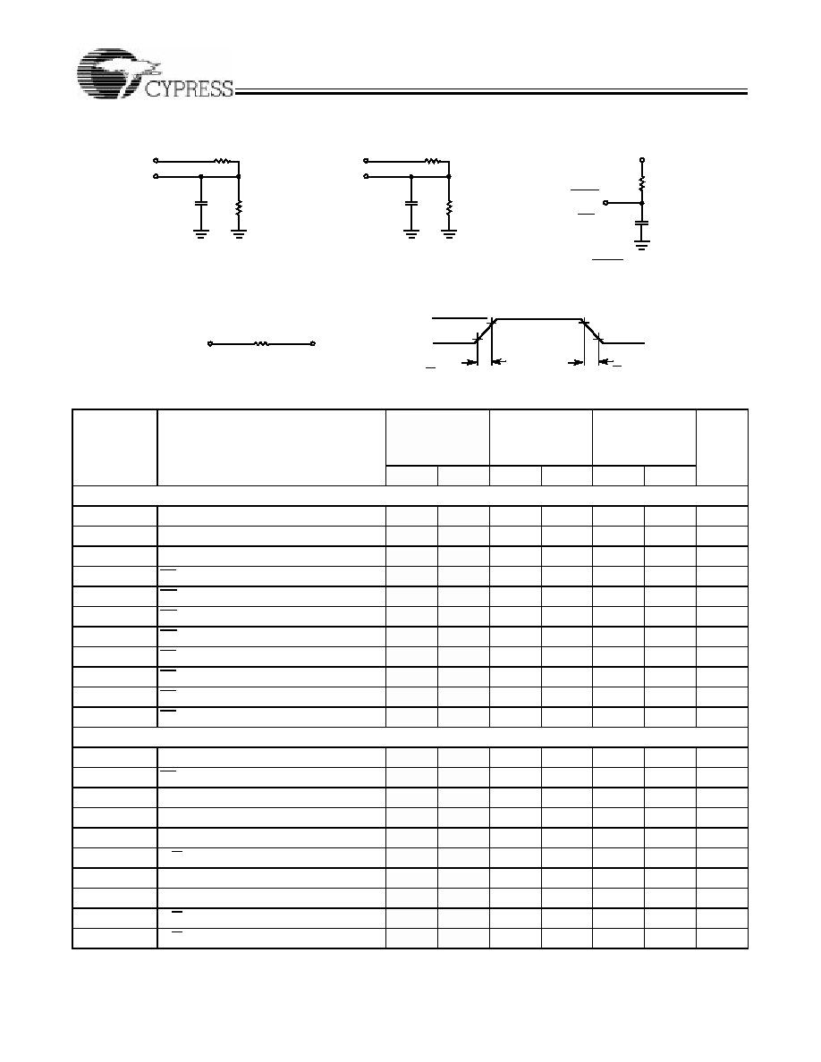
AC Test Loads and Waveforms
3.0V
5V
OUTPUT
R1893
R2
347
30 pF
INCLUDING
JIGAND
SCOPE
GND
90%
90%
10%
< 5 ns
< 5 ns
5V
OUTPUT
C132-5
R1893
R2
347
5 pF
INCLUDING
JIGAND
SCOPE
C132-6
(a)
(b)
OUTPUT
1.4V
Equivalent to:
TH V…NIN EQUIVALENT
5V
281
30pF
BUSY
OR
INT
BUSYOutput Load
(CY7C132/CY7C136 ONLY)
10%
ALL INPUT PULSES
250
Switching Characteristics
Over the Operating Range
[6, 11]
Parameter
Description
7C136-15
[3,4]
7C146-15
7C132-25
[3]
7C136-25
7C142-25
7C146-25
7C132-30
7C136-30
7C142-30
7C146-30
Unit
Min.
Max.
Min.
Max.
Min.
Max.
READ CYCLE
t
RC
Read Cycle Time
15
25
30
ns
t
AA
Address to Data Valid
[12]
15
25
30
ns
t
OHA
Data Hold from Address Change
0
0
0
ns
t
ACE
CE LOW to Data Valid
[12]
15
25
30
ns
t
DOE
OE LOW to Data Valid
[12]
10
15
20
ns
t
LZOE
OE LOW to Low Z
[10, 13]
3
3
3
ns
t
HZOE
OE HIGH to High Z
[10, 13, 14]
10
15
15
ns
t
LZCE
CE LOW to Low Z
[10, 13]
3
5
5
ns
t
HZCE
CE HIGH to High Z
[10, 13, 14]
10
15
15
ns
t
PU
CE LOW to Power-Up
[10]
0
0
0
ns
t
PD
CE HIGH to Power-Down
[10]
15
25
25
ns
WRITE CYCLE
[15]
t
WC
Write Cycle Time
15
25
30
ns
t
SCE
CE LOW to Write End
12
20
25
ns
t
AW
Address Set-Up to Write End
12
20
25
ns
t
HA
Address Hold from Write End
2
2
2
ns
t
SA
Address Set-Up to Write Start
0
0
0
ns
t
PWE
R/W Pulse Width
12
15
25
ns
t
SD
Data Set-Up to Write End
10
15
15
ns
t
HD
Data Hold from Write End
0
0
0
ns
t
HZWE
R/W LOW to High Z
[10]
10
15
15
ns
t
LZWE
R/W HIGH to Low Z
[10]
0
0
0
ns

CY7C132/CY7C136
CY7C142/CY7C146
5
BUSY/INTERRUPT TIMING
t
BLA
BUSY LOW from Address Match
15
20
20
ns
t
BHA
BUSY HIGH from Address Mismatch
[16]
15
20
20
ns
t
BLC
BUSY LOW from CE LOW
15
20
20
ns
t
BHC
BUSY HIGH from CE HIGH
[16]
15
20
20
ns
t
PS
Port Set Up for Priority
5
5
5
ns
t
WB
R/W LOW after BUSY LOW
[17]
0
0
0
ns
t
WH
R/W HIGH after BUSY HIGH
13
20
30
ns
t
BDD
BUSY HIGH to Valid Data
15
25
30
ns
t
DDD
Write Data Valid to Read Data Valid
Note
18
Note
18
Note
18
ns
t
WDD
Write Pulse to Data Delay
Note
18
Note
18
Note
18
ns
INTERRUPT TIMING
[19]
t
WINS
R/W to INTERRUPT Set Time
15
25
25
ns
t
EINS
CE to INTERRUPT Set Time
15
25
25
ns
t
INS
Address to INTERRUPT Set Time
15
25
25
ns
t
OINR
OE to INTERRUPT Reset Time
[16]
15
25
25
ns
t
EINR
CE to INTERRUPT Reset Time
[16]
15
25
25
ns
t
INR
Address to INTERRUPT Reset Time
[16]
15
25
25
ns
Switching Characteristics
Over the Operating Range
[6, 11]
(continued)
Parameter
Description
7C136-15
[3,4]
7C146-15
7C132-25
[3]
7C136-25
7C142-25
7C146-25
7C132-30
7C136-30
7C142-30
7C146-30
Unit
Min.
Max.
Min.
Max.
Min.
Max.
Switching Characteristics
Over the Operating Range
[6, 11]
7C132-35
7C136-35
7C142-35
7C146-35
7C132-45
7C136-45
7C142-45
7C146-45
7C132-55
7C136-55
7C142-55
7C146-55
Parameter
Description
Min.
Max.
Min.
Max.
Min.
Max.
Unit
READ CYCLE
t
RC
Read Cycle Time
35
45
55
ns
t
AA
Address to Data Valid
[12]
35
45
55
ns
t
OHA
Data Hold from Address Change
0
0
0
ns
t
ACE
CE LOW to Data Valid
[12]
35
45
55
ns
t
DOE
OE LOW to Data Valid
[12]
20
25
25
ns
t
LZOE
OE LOW to Low Z
[10, 13]
3
3
3
ns
t
HZOE
OE HIGH to High Z
[10, 13, 14]
20
20
25
ns
t
LZCE
CE LOW to Low Z
[10, 13]
5
5
5
ns
t
HZCE
CE HIGH to High Z
[10, 13, 14]
20
20
25
ns
t
PU
CE LOW to Power-Up
[10]
0
0
0
ns
t
PD
CE HIGH to Power-Down
[10]
35
35
35
ns

CY7C132/CY7C136
CY7C142/CY7C146
6
WRITE CYCLE
[15]
t
WC
Write Cycle Time
35
45
55
ns
t
SCE
CE LOW to Write End
30
35
40
ns
t
AW
Address Set-Up to Write End
30
35
40
ns
t
HA
Address Hold from Write End
2
2
2
ns
t
SA
Address Set-Up to Write Start
0
0
0
ns
t
PWE
R/W Pulse Width
25
30
30
ns
t
SD
Data Set-Up to Write End
15
20
20
ns
t
HD
Data Hold from Write End
0
0
0
ns
t
HZWE
R/W LOW to High Z
[10]
20
20
25
ns
t
LZWE
R/W HIGH to Low Z
[10]
0
0
0
ns
BUSY/INTERRUPT TIMING
t
BLA
BUSY LOW from Address Match
20
25
30
ns
t
BHA
BUSY HIGH from Address Mismatch
[16]
20
25
30
ns
t
BLC
BUSY LOW from CE LOW
20
25
30
ns
t
BHC
BUSY HIGH from CE HIGH
[16]
20
25
30
ns
t
PS
Port Set Up for Priority
5
5
5
ns
t
WB
R/W LOW after BUSY LOW
[17]
0
0
0
ns
t
WH
R/W HIGH after BUSY HIGH
30
35
35
ns
t
BDD
BUSY HIGH to Valid Data
35
45
45
ns
t
DDD
Write Data Valid to Read Data Valid
Note
18
Note
18
Note
18
ns
t
WDD
Write Pulse to Data Delay
Note
18
Note
18
Note
18
ns
INTERRUPT TIMING
[19]
t
WINS
R/W to INTERRUPT Set Time
25
35
45
ns
t
EINS
CE to INTERRUPT Set Time
25
35
45
ns
t
INS
Address to INTERRUPT Set
Time 25
35
45
ns
t
OINR
OE to INTERRUPT Reset Time
[16]
25
35
45
ns
t
EINR
CE to INTERRUPT Reset Time
[16]
25
35
45
ns
t
INR
Address to INTERRUPT Reset Time
[16]
25
35
45
ns
Notes:
11.
Test conditions assume signal transition times of 5 ns or less, timing reference levels of 1.5V, input pulse levels of 0 to 3.0V and output loading of the specified
I
OL
/I
OH,
and 30-pF load capacitance.
12. AC test conditions use V
OH
= 1.6V and V
OL
= 1.4V.
13. At any given temperature and voltage condition for any given device, t
HZCE
is less than t
LZCE
and t
HZOE
is less than t
LZOE
.
14. t
LZCE
, t
LZWE
, t
HZOE
, t
LZOE,
t
HZCE,
and t
HZWE
are tested with C
L
= 5pF as in part (b) of AC Test Loads
. Transition is measured ±500 mV from steady-state voltage.
15. The internal write time of the memory is defined by the overlap of CE LOW and R/W LOW. Both signals must be LOW to initiate a write and either signal can terminate
a write by going HIGH. The data input setup and hold timing should be referenced to the rising edge of the signal that terminates the write.
16. These parameters are measured from the input signal changing, until the output pin goes to a high-impedance state.
17. CY7C142/CY7C146 only.
18. A write operation on Port A, where Port A has priority, leaves the data on Port B's outputs undisturbed until one access time after one of the following:
BUSY on Port B goes HIGH.
Port B's address toggled.
CE for Port B is toggled.
R/W for Port B is toggled during valid read.
19. 52-pin PLCC and PQFP versions only.
Switching Characteristics
Over the Operating Range
[6, 11]
(continued)
7C132-35
7C136-35
7C142-35
7C146-35
7C132-45
7C136-45
7C142-45
7C146-45
7C132-55
7C136-55
7C142-55
7C146-55

CY7C132/CY7C136
CY7C142/CY7C146
7
Switching Waveforms
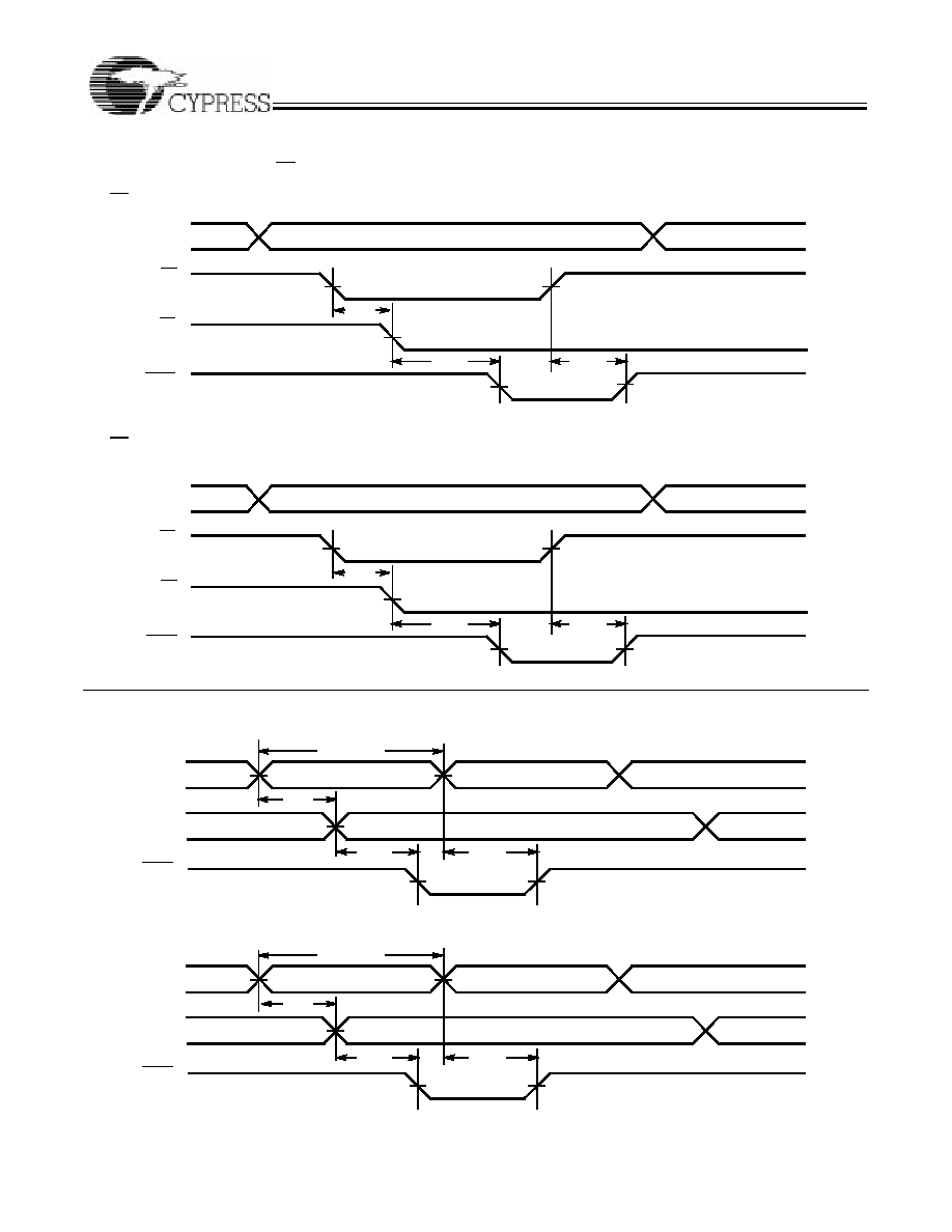
Read Cycle No. 1 (Either Port-Address Access)
[20, 21]
Read Cycle No. 2 (Either Port-CE/OE)
[20, 22]
Read Cycle No. 3 (Read with BUSY Master: CY7C132 and CY7C136)
n
Notes:
20. R/W is HIGH for read cycle.
21. Device is continuously selected, CE = V
IL
and OE =
V
IL
.
22. Address valid prior to or coincident with CE transition LOW.
t
RC
t
AA
t
OHA
DATA VALID
PREVIOUS DATA VALID
DATA OUT
ADDRESS
C132-7
t
ACE
t
LZOE
t
DOE
t
HZOE
t
HZCE
DATA VALID
DATA OUT
CE
OE
t
LZCE
t
PU
I
CC
I
SB
t
PD
C132-8
t
BHA
t
BDD
VALID
t
DDD
t
WDD
ADDRESS MATCH
ADDRESS MATCH
R/W
R
ADDRESS
R
D
INR
ADDRESS
L
BUSY
L
DOUT
L
C132-9
t
PS
t
BLA
t
RC
t
PWE
VALID

CY7C132/CY7C136
CY7C142/CY7C146
8
Write Cycle No.1 (OE Three-States Data I/Os-Either Port)
[15, 23]
Write Cycle No. 2 (R/W Three≠States Data I/Os-Either Port)
[15, 24]
Notes:
23. If OE is LOW during a R/W controlled write cycle, the write pulse width must be the larger of t
PWE
or t
HZWE
+ t
SD
to allow the data I/O pins to enter high impedance and for data
to be placed on the bus for the required t
SD
.
24. If the CE LOW transition occurs simultaneously with or after the R/W LOW transition, the outputs remain in a high-impedance state.
Switching Waveforms
(continued)
t
AW
t
WC
DATA VALID
HIGH IMPEDANCE
t
SCE
t
SA
t
PWE
t
HD
t
SD
t
HA
t
HZOE
CE
R/W
ADDRESS
OE
D
OUT
DATA
IN
C132-10
t
AW
t
WC
t
SCE
t
SA
t
PWE
t
HD
t
SD
t
HZWE
t
HA
HIGH IMPEDANCE
CE
R/W
ADDRESS
D
OUT
DATA
IN
t
LZWE
DATA VALID
C132-11
CY7C132/CY7C136
CY7C142/CY7C146
9
Busy Timing Diagram No. 1 (CE Arbitration)
Busy Timing Diagram No. 2 (Address Arbitration)
Switching Waveforms
(continued)
ADDRESS MATCH
t
PS
CE
L
Valid First:
t
BLC
t
BHC
ADDRESS MATCH
t
PS
t
BLC
t
BHC
CE
R
Valid First:
C132-12
C132-13
BUSY
L
CE
R
CE
L
ADDRESS
L,R
BUSY
R
CE
L
CE
R
ADDRESS
L,R
Left AddressValid First:
ADDRESS MATCH
t
PS
ADDRESS
L
BUSY
R
ADDRESS MISMATCH
t
RC
or t
WC
t
BLA
t
BHA
ADDRESS
R
ADDRESS MATCH
ADDRESS MISMATCH
t
PS
ADDRESS
L
BUSY
L
t
RC
or t
WC
t
BLA
t
BHA
ADDRESS
R
Right Address Valid First:
C132-14
C132-15

CY7C132/CY7C136
CY7C142/CY7C146
10
Busy Timing Diagram No. 3 (Write with BUSY, Slave: CY7C142/CY7C146)
Interrupt Timing Diagrams
[19]
Left Side Sets INT
R
:
Right Side Clears INT
R
:
Switching Waveforms
(continued)
t
PWE
t
WB
t
WH
BUSY
C132-16
R/W
CE
WRITE 7FF
t
INS
ADDRESS
L
R/W
L
t
WC
t
EINS
CE
L
t
HA
t
SA
t
WINS
INT
R
C132-17
READ 7FF
t
RC
t
EINR
t
HA
t
INR
t
OINR
ADDRESS
R
CE
R
R/W
R
INT
R
OE
R
C132-18

CY7C132/CY7C136
CY7C142/CY7C146
11
Right Side Sets INT
L
:
Right Side Clears INT
L
:
Interrupt Timing Diagrams
[19]
(continued)
WRITE 7FE
t
INS
ADDRESS
R
R/W
R
t
WC
t
EINS
CE
R
t
HA
t
SA
t
WINS
INT
L
C132-19
READ 7FE
t
EINR
t
HA
t
INR
t
OINR
ADDRESS
L
CE
L
R/W
L
INT
L
OE
L
t
RC
C132-20

CY7C132/CY7C136
CY7C142/CY7C146
12
Typical DC and AC Characteristics
1.4
1.0
0.4
4.0
4.5
5.0
5.5
6.0
-55
25
125
1.2
1.0
120
100
80
60
40
20
0
1.0
2.0
3.0
4.0
SUPPLYVOLTAGE(V)
NORMALIZED SUPPLY CURRENT
vs. SUPPLY VOLTAGE
NORMALIZED SUPPLY CURRENT
vs. AMBIENT TEMPERATURE
AMBIENTTEMPERATURE(∞C)
OUTPUTVOLTAGE(V)
OUTPUT SOURCE CURRENT
vs. OUTPUT VOLTAGE
0.0
0.8
0.8
0.6
0.6
V
CC
=5.0V
V
IN
=5.0V
V
CC
=5.0V
T
A
=25∞C
0
I
CC
I
CC
1.6
1.4
1.2
1.0
0.8
-55
125
NORMALIZED ACCESS TIME
vs. AMBIENT TEMPERATURE
AMBIENTTEMPERATURE(∞C)
1.4
1.3
1.2
1.0
0.9
4.0
4.5
5.0
5.5
6.0
SUPPLYVOLTAGE(V)
NORMALIZED ACCESS TIME
vs. SUPPLY VOLTAGE
120
140
100
60
40
20
0.0
1.0
2.0
3.0
4.0
0
80
OUTPUTVOLTAGE(V)
OUTPUT SINK CURRENT
vs. OUTPUT VOLTAGE
V
CC
=5.0V
T
A
=25∞C
0.6
0.8
V
CC
=5.0V
T
A
=25∞C
1.25
1.0
0.75
10
40
0.50
NORMALIZED I
CC
vs. CYCLE TIME
CYCLE FREQUENCY (MHz)
3.0
2.5
2.0
1.5
0.5
0
1.0
2.0
3.0
5.0
25.0
30.0
20.0
10.0
5.0
0
200
400
600
800
0
15.0
0.0
SUPPLYVOLTAGE(V)
TYPICAL POWER- ON CURRENT
vs. SUPPLY VOLTAGE
CAPACITANCE(pF)
TYPICAL ACCESS TIME CHANGE
vs. OUTPUT LOADING
4.0
1000
1.0
20
30
0.2
0.6
1.2
I
SB3
0.2
0.4
I
SB3
25
1.1
V
CC
=4.5V
T
A
=25∞C
V
CC
=5.0V
T
A
=25∞C
V
IN
=0.5V

CY7C132/CY7C136
CY7C142/CY7C146
13
Shaded area contains preliminary information.
Ordering Information
Speed
(ns)
Ordering Code
Package
Name
Package Type
Operating
Range
30
CY7C132-30PC
P25
48-Lead (600-Mil) Molded DIP
Commercial
CY7C132-30PI
P25
48-Lead (600-Mil) Molded DIP
Industrial
35
CY7C132-35PC
P25
48-Lead (600-Mil) Molded DIP
Commercial
CY7C132-35PI
P25
48-Lead (600-Mil) Molded DIP
Industrial
CY7C132-35DMB
D26
48-Lead (600-Mil) Sidebraze DIP
Military
45
CY7C132-45PC
P25
48-Lead (600-Mil) Molded DIP
Commercial
CY7C132-45PI
P25
48-Lead (600-Mil) Molded DIP
Industrial
CY7C132-45DMB
D26
48-Lead (600-Mil) Sidebraze DIP
Military
55
CY7C132-55PC
P25
48-Lead (600-Mil) Molded DIP
Commercial
CY7C132-55PI
P25
48-Lead (600-Mil) Molded DIP
Industrial
CY7C132-55DMB
D26
48-Lead (600-Mil) Sidebraze DIP
Military
Speed
(ns)
Ordering Code
Package
Name
Package Type
Operating
Range
15
CY7C136-15JC
J69
52-Lead Plastic Leaded Chip Carrier
Commercial
CY7C136-15NC
N52
52-Pin Plastic Quad Flatpack
25
CY7C136-25JC
J69
52-Lead Plastic Leaded Chip Carrier
Commercial
CY7C136-25NC
N52
52-Pin Plastic Quad Flatpack
30
CY7C136-30JC
J69
52-Lead Plastic Leaded Chip Carrier
Commercial
CY7C136-30NC
N52
52-Pin Plastic Quad Flatpack
CY7C136-30JI
J69
52-Lead Plastic Leaded Chip Carrier
Industrial
35
CY7C136-35JC
J69
52-Lead Plastic Leaded Chip Carrier
Commercial
CY7C136-35NC
N52
52-Pin Plastic Quad Flatpack
CY7C136-35JI
J69
52-Lead Plastic Leaded Chip Carrier
Industrial
CY7C136-35LMB
L69
52-Square Leadless Chip Carrier
Military
45
CY7C136-45JC
J69
52-Lead Plastic Leaded Chip Carrier
Commercial
CY7C136-45NC
N52
52-Pin Plastic Quad Flatpack
CY7C136-45JI
J69
52-Lead Plastic Leaded Chip Carrier
Industrial
CY7C136-45LMB
L69
52-Square Leadless Chip Carrier
Military
55
CY7C136-55JC
J69
52-Lead Plastic Leaded Chip Carrier
Commercial
CY7C136-55NC
N52
52-Pin Plastic Quad Flatpack
CY7C136-55JI
J69
52-Lead Plastic Leaded Chip Carrier
Industrial
CY7C136-55LMB
L69
52-Square Leadless Chip Carrier
Military
CY7C132/CY7C136
CY7C142/CY7C146
14
Ordering Information
(continued)
Shaded area contains preliminary information.
Speed
(ns)
Ordering Code
Package
Name
Package Type
Operating
Range
30
CY7C142-30PC
P25
48-Lead (600-Mil) Molded DIP
Commercial
CY7C142-30PI
P25
48-Lead (600-Mil) Molded DIP
Industrial
35
CY7C142-35PC
P25
48-Lead (600-Mil) Molded DIP
Commercial
CY7C142-35PI
P25
48-Lead (600-Mil) Molded DIP
Industrial
CY7C142-35DMB
D26
48-Lead (600-Mil) Sidebraze DIP
Military
45
CY7C142-45PC
P25
48-Lead (600-Mil) Molded DIP
Commercial
CY7C142-45PI
P25
48-Lead (600-Mil) Molded DIP
Industrial
CY7C142-45DMB
D26
48-Lead (600-Mil) Sidebraze DIP
Military
55
CY7C142-55PC
P25
48-Lead (600-Mil) Molded DIP
Commercial
CY7C142-55PI
P25
48-Lead (600-Mil) Molded DIP
Industrial
CY7C142-55DMB
D26
48-Lead (600-Mil) Sidebraze DIP
Military
Speed
(ns)
Ordering Code
Package
Name
Package Type
Operating
Range
15
CY7C136-15JC
J69
52-Lead Plastic Leaded Chip Carrier
Commercial
CY7C136-15NC
N52
52-Pin Plastic Quad Flatpack
25
CY7C146-25JC
J69
52-Lead Plastic Leaded Chip Carrier
Commercial
CY7C146-25NC
N52
52-Pin Plastic Quad Flatpack
30
CY7C146-30JC
J69
52-Lead Plastic Leaded Chip Carrier
Commercial
CY7C146-30NC
N52
52-Pin Plastic Quad Flatpack
CY7C146-30JI
J69
52-Lead Plastic Leaded Chip Carrier
Industrial
35
CY7C146-35JC
J69
52-Lead Plastic Leaded Chip Carrier
Commercial
CY7C146-35NC
N52
52-Pin Plastic Quad Flatpack
CY7C146-35JI
J69
52-Lead Plastic Leaded Chip Carrier
Industrial
CY7C146-35LMB
L69
52-Square Leadless Chip Carrier
Military
45
CY7C146-45JC
J69
52-Lead Plastic Leaded Chip Carrier
Commercial
CY7C146-45NC
N52
52-Pin Plastic Quad Flatpack
CY7C146-45JI
J69
52-Lead Plastic Leaded Chip Carrier
Industrial
CY7C146-45LMB
L69
52-Square Leadless Chip Carrier
Military
55
CY7C146-55JC
J69
52-Lead Plastic Leaded Chip Carrier
Commercial
CY7C146-55NC
N52
52-Pin Plastic Quad Flatpack
CY7C146-55JI
J69
52-Lead Plastic Leaded Chip Carrier
Industrial
CY7C146-55LMB
L69
52-Square Leadless Chip Carrier
Military

CY7C132/CY7C136
CY7C142/CY7C146
15
MILITARY SPECIFICATIONS
Group A Subgroup Testing
DC Characteristics
Switching Characteristics
Parameter
Subgroups
V
OH
1, 2, 3
V
OL
1, 2, 3
V
IH
1, 2, 3
V
IL
Max.
1, 2, 3
I
IX
1, 2, 3
I
OZ
1, 2, 3
I
CC
1, 2, 3
I
SB1
1, 2, 3
I
SB2
1, 2, 3
I
SB3
1, 2, 3
I
SB4
1, 2, 3
Parameter
Subgroups
READ CYCLE
t
RC
7, 8, 9, 10, 11
t
AA
7, 8, 9, 10, 11
t
ACE
7, 8, 9, 10, 11
t
DOE
7, 8, 9, 10, 11
WRITE CYCLE
t
WC
7, 8, 9, 10, 11
t
SCE
7, 8, 9, 10, 11
t
AW
7, 8, 9, 10, 11
t
HA
7, 8, 9, 10, 11
t
SA
7, 8, 9, 10, 11
t
PWE
7, 8, 9, 10, 11
t
SD
7, 8, 9, 10, 11
t
HD
7, 8, 9, 10, 11
BUSY/INTERRUPT TIMING
t
BLA
7, 8, 9, 10, 11
t
BHA
7, 8, 9, 10, 11
t
BLC
7, 8, 9, 10, 11
t
BHC
7, 8, 9, 10, 11
t
PS
7, 8, 9, 10, 11
t
WINS
7, 8, 9, 10, 11
t
EINS
7, 8, 9, 10, 11
t
INS
7, 8, 9, 10, 11
t
OINR
7, 8, 9, 10, 11
t
EINR
7, 8, 9, 10, 11
t
INR
7, 8, 9, 10, 11
BUSY TIMING
t
WB
[25]
7, 8, 9, 10, 11
t
WH
7, 8, 9, 10, 11
t
BDD
7, 8, 9, 10, 11
Note:
25. CY7C142/CY7C146 only.
Document #: 38-00061-K
CY7C132/CY7C136
CY7C142/CY7C146
16
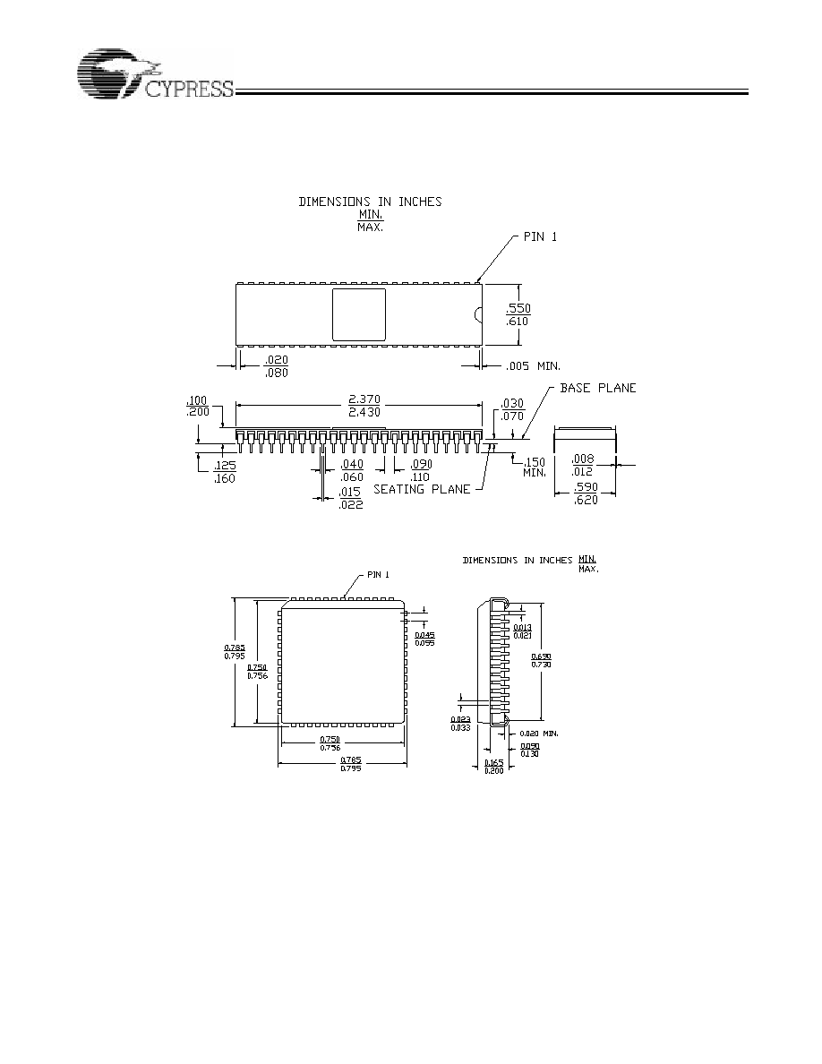
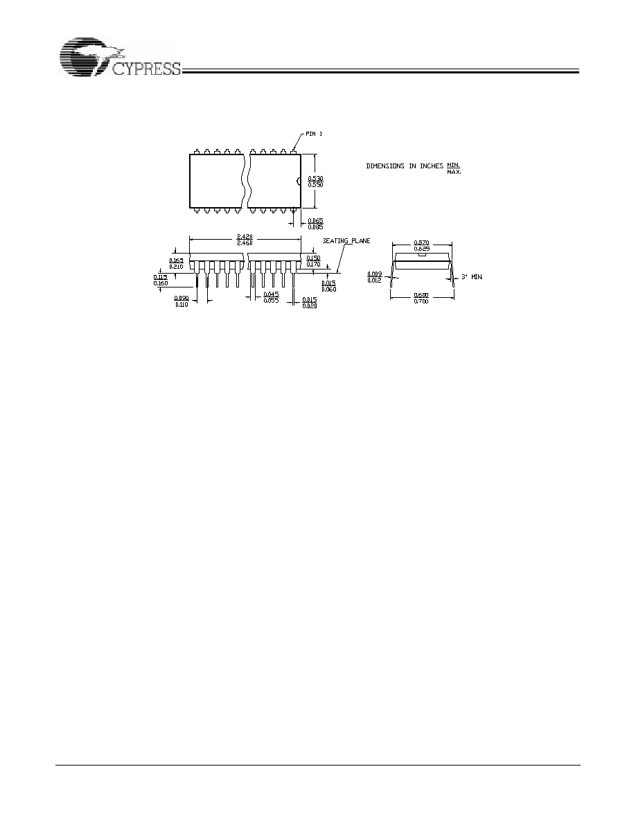
Package Diagrams
48-Lead (600-Mil) Sidebraze DIP D26
52-Lead Plastic Leaded Chip Carrier J69

CY7C132/CY7C136
CY7C142/CY7C146
17
52-Square Leadless Chip Carrier L69
52-Lead Plastic Quad Flatpack N52
Package Diagrams
(continued)
CY7C132/CY7C136
CY7C142/CY7C146
© Cypress Semiconductor Corporation, 1997. The information contained herein is subject to change without notice. Cypress Semiconductor Corporation assumes no responsibility for the use
of any circuitry other than circuitry embodied in a Cypress Semiconductor product. Nor does it convey or imply any license under patent or other rights. Cypress Semiconductor does not authorize
its products for use as critical components in life-support systems where a malfunction or failure may reasonably be expected to result in significant injury to the user. The inclusion of Cypress
Semiconductor products in life-support systems application implies that the manufacturer assumes all risk of such use and in doing so indemnifies Cypress Semiconductor against all charges.
48-Lead (600-Mil) Molded DIP P25
Package Diagrams
(continued)