 | –≠–ª–µ–∫—Ç—Ä–æ–Ω–Ω—ã–π –∫–æ–º–ø–æ–Ω–µ–Ω—Ç: B9940L | –°–∫–∞—á–∞—Ç—å:  PDF PDF  ZIP ZIP |

2.5V or 3.3V, 200-MHz, 1:18 Clock Distribution Buffer
B9940L
Cypress Semiconductor Corporation
∑
3901 North First Street
∑
San Jose
,
CA 95134
∑
408-943-2600
Document #: 38-07105 Rev. *C
Revised December 26, 2002
Features
∑ 200-MHz clock support
∑ LVPECL or LVCMOS/LVTTL clock input
∑ LVCMOS/LVTTL compatible inputs
∑ 18 clock outputs: drive up to 36 clock lines
∑ 150-ps max. output-to-output skew
∑ Dual- or single-supply operation:
-- 3.3V core and 3.3V outputs
-- 3.3V core and 2.5V outputs
-- 2.5V core and 2.5V outputs
∑ Pin-compatible with MPC940L
∑ Industrial temperature range: -40∞C to 85∞C
∑ 32-pin LQFP package
Description
The B9940L is a low-voltage clock distribution buffer with the
capability to select either a differential LVPECL- or an
LVCMOS/LVTTL-compatible input clock. The two clock
sources can be used to provide for a test clock as well as the
primary system clock. All other control inputs are
LVCMOS/LVTTL compatible. The eighteen outputs are 2.5V or
3.3V compatible and can drive two series-terminated 50
transmission lines. With this capability the B9940L has an
effective fan-out of 1:36. Low output-to-output skews make the
B9940L an ideal clock distribution buffer for nested clock trees
in the most demanding of synchronous systems.
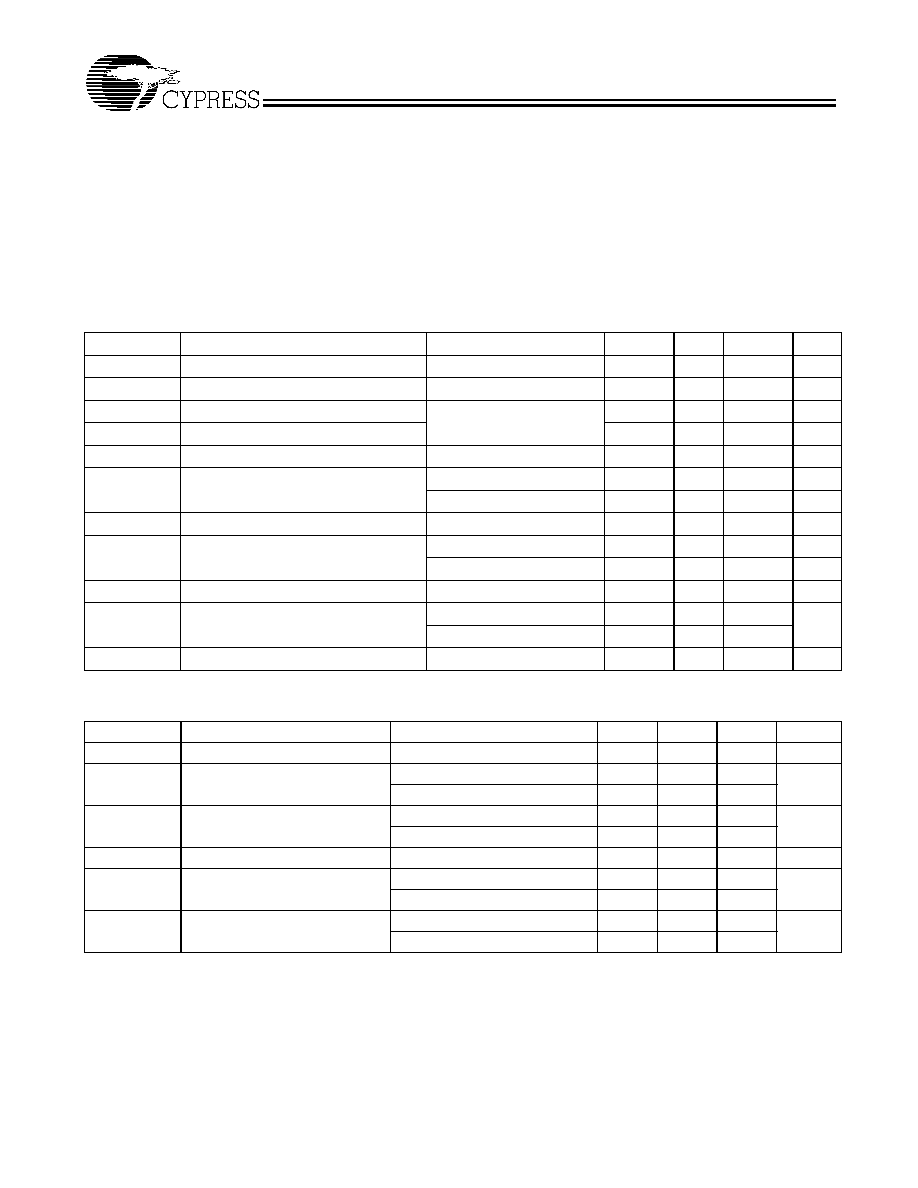
Block Diagram
Pin Configuration
B 9940L
Q0
Q1
Q2
VD
D
C
Q3
Q4
Q5
VS
S
Q1
7
Q1
6
Q1
5
VSS
Q1
4
Q1
3
Q1
2
VD
D
C
Q 6
Q 7
Q 8
V D D
Q 9
Q 10
Q 11
V S S
V S S
V S S
T C L K
T C LK _S E L
P E C L _C L K
P E C L_ C LK #
V D D
V D D C
1
2
3
4
5
6
7
8
24
23
22
21
20
19
18
17
9
10
11
12
13
14
15
16
32
31
30
29
28
27
26
25
PECL_CLK
PECL_CLK#
0
1
TCLK
TCLK_SEL
VDDC
18
Q0-Q17
VDD

B9940L
Document #: 38-07105 Rev. *C
Page 2 of 5
Note:
1.
PD = internal pull-down, PU = internal pull-up.
Pin Description
[1]
Pin
Name
PWR
I/O
Description
5
PECL_CLK
I, PU PECL Input Clock
6
PECL_CLK#
I, PD PECL Input Clock
3
TCLK
I, PD External Reference/Test Clock Input
9, 10, 11, 13,
14, 15, 18, 19,
20, 22, 23, 24,
26, 27, 28, 30,
31, 32
Q(17:0)
VDDC
O
Clock Outputs
4
TCLK_SEL
I, PD Clock Select Input. When LOW, PECL clock is selected and when
HIGH TCLK is selected.
8, 16, 29
VDDC
3.3V or 2.5V Power Supply for Output Clock Buffers
7, 21
VDD
3.3V or 2.5V Power Supply
1, 2, 12, 17, 25 VSS
Common Ground
B9940L
Document #: 38-07105 Rev. *C
Page 3 of 5
Maximum Ratings
[2]
Maximum Input Voltage Relative to V
SS
: ............ V
SS
≠ 0.3V
Maximum Input Voltage Relative to V
DD
:............. V
DD
+ 0.3V
Storage Temperature: ................................≠65
∞
C to + 150
∞
C
Operating Temperature: ................................ ≠40
∞
C to +85
∞
C
Maximum ESD protection ...............................................2 kV
Maximum Power Supply: ................................................5.5V
Maximum Input Current: ............................................±20 mA
This device contains circuitry to protect the inputs against
damage due to high static voltages or electric field; however,
precautions should be taken to avoid application of any
voltage higher than the maximum rated voltages to this circuit.
For proper operation, V
in
and V
out
should be constrained to the
range:
V
SS
< (V
in
or V
out
) < V
DD
.
Unused inputs must always be tied to an appropriate logic
voltage level (either V
SS
or V
DD
).
DC Parameters
V
DD
= 3.3V ±5% or 2.5V ±5%, V
DDC
= 3.3V ±5% or 2.5V ±5%, T
A
= ≠40∞C to +85∞C
Parameter
Description
Conditions
Min.
Typ.
Max.
Unit
V
IL
Input Low Voltage
All other inputs
V
SS
≠
0.8
V
V
IH
Input High Voltage
All other inputs
2.0
≠
V
DD
V
I
IL
Input Low Current
[3]
≠
≠
≠200
µA
I
IH
Input High Current
[3]
≠
≠
200
µA
V
PP
Peak-to-Peak Input Voltage PECL_CLK
500
≠
1000
mV
V
CMR
Common Mode Range
[4]
PECL_CLK
V
DD
= 3.3V
V
DD
≠ 1.4
≠
V
DD
≠ 0.6
V
V
DD
= 2.5V
V
DD
≠ 1.0
≠
V
DD
≠ 0.6
V
V
OL
Output Low Voltage
[5]
I
OL
= 20 mA
≠
≠
0.5
V
V
OH
Output High Voltage
[5]
I
OH
= ≠20 mA, V
DDC
= 3.3V
2.4
≠
≠
V
I
OH
= ≠20 mA, V
DDC
= 2.5V
1.8
≠
≠
V
I
DDQ
Quiescent Supply Current
≠
2
5
mA
Z
out
Output Impedance
V
DD
= 3.3V
9
14
19
V
DD
= 2.5V
11
18
26
C
in
Input Capacitance
≠
4
≠
pF
AC Parameters
V
DD
= 3.3V ±5% or 2.5V ±5%, V
DDC
= 3.3V ±5% or 2.5V ±5%, T
A
= ≠40∞C to +85∞C
[6]
Parameter
Description
Conditions
Min.
Typ.
Max.
Units
F
max
Maximum Input Frequency
≠
≠
200
MHz
t
PD
PECL_CLK to Q Delay
[7, 9]
V
DD
= 3.3V
2.0
3.5
4.0
ns
V
DD
= 2.5V
2.6
4.0
5.2
t
PD
TTL_CLK to Q Delay
[7, 9]
V
DD
= 3.3V
1.8
3.3
3.8
ns
V
DD
= 2.5V
2.3
3.8
4.4
FoutDC
Output Duty Cycle
[7, 8, 9]
Measured at V
DD
/2
45
≠
55
%
T
skew
Output-to-Output Skew
[7, 9]
V
DD
= 3.3V, Fin = 150 MHz
≠
≠
150
ps
V
DD
= 2.5V, Fin = 150 MHz
≠
≠
200
T
skew
(pp)
Part-to-Part Skew
[10]
PECL, V
DDC
= 3.3V
≠
≠
1.4
ns
PECL, V
DDC
= 2.5V
≠
≠
2.2
Notes:
2.
The voltage on any input or I/O pin cannot exceed the power pin during power-up. Power suppl sequencing is NOT required.
3.
Inputs have pull-up/pull-down resistors that effect input current.
4.
The V
CMR
is the difference from the most positive side of the differential input signal. Normal operation is obtained when the "High" input is within the V
CMR
range and the input lies within the V
PP
specification.
5.
Driving series or parallel terminated 50
(or 50
to V
DD
/2) transmission lines.
6.
Parameters are guaranteed by design and characterization. Not 100% tested in production. All parameters specified with loaded outputs.
7.
Outputs driving 50
transmission lines.
8.
50% input duty cycle.
9.
Outputs loaded with 30 pF each.
10. Across temperature and voltage ranges, includes output skew.

B9940L
Document #: 38-07105 Rev. *C
Page 4 of 5
© Cypress Semiconductor Corporation, 2002. The information contained herein is subject to change without notice. Cypress Semiconductor Corporation assumes no responsibility for the use
of any circuitry other than circuitry embodied in a Cypress Semiconductor product. Nor does it convey or imply any license under patent or other rights. Cypress Semiconductor does not authorize
its products for use as critical components in life-support systems where a malfunction or failure may reasonably be expected to result in significant injury to the user. The inclusion of Cypress
Semiconductor products in life-support systems application implies that the manufacturer assumes all risk of such use and in doing so indemnifies Cypress Semiconductor against all charges.
Ordering Information
Package Drawing and Dimensions
All product and company names mentioned in this document may be the trademarks of their respective holders.
Note:
11. For a specific temperature and voltage, includes output skew.
T
skew
(pp)
Part-to-Part Skew
[10]
TCLK, V
DDC
= 3.3V
≠
≠
1.2
ns
TCLK, V
DDC
= 2.5V
≠
≠
1.7
T
skew
(pp)
Part to Part Skew
[11]
PECL_CLK
≠
≠
850
ps
TCLK
≠
≠
750
t
R
/t
F
Output Clocks Rise/Fall Time
[7, 9]
0.7V to 2.0V, V
DDC
= 3.3V
0.3
≠
1.1
ns
0.5V to 1.8V, V
DDC
= 2.5V
0.3
≠
1.2
AC Parameters
V
DD
= 3.3V ±5% or 2.5V ±5%, V
DDC
= 3.3V ±5% or 2.5V ±5%, T
A
= ≠40∞C to +85∞C (continued)
[6]
Parameter
Description
Conditions
Min.
Typ.
Max.
Units
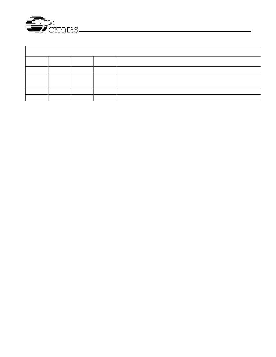
Part Number
Package Type
Production Flow
IMIB9940LBL
32-pin LQFP
Industrial, ≠40∞C to +85∞C
IMIB9940LBLT
32-pin LQFP≠Tape and Reel
Industrial, ≠40∞C to +85∞C
32-lead Thin Plastic Quad Flatpack 7 x 7 x 1.4 mm A32.14
51-85088-*B
B9940L
Document #: 38-07105 Rev. *C
Page 5 of 5
Document History Page
Document Title: B9940L 2.5V or 3.3V, 200-MHz, 1:18 Clock Distribution Buffer
Document Number: 38-07105
REV.
ECN NO.
Issue
Date
Orig. of
Change
Description of Change
**
107509
06/14/01
NDP
Convert from IMI to Cypress
*A
116093
09/09/02
HWT
Converted from Word Doc to Framemaker
Corrected the Ordering Information to match the DevMaster
Corrected Output Impedance Type to 9/11,14/18, and 19/26 in DC parameters
*B
120824
11/21/02
RGL
Corrected minor typo
*C
122783
12/26/02
RBI
Add power up requirements to maximum ratings information