 | –≠–ª–µ–∫—Ç—Ä–æ–Ω–Ω—ã–π –∫–æ–º–ø–æ–Ω–µ–Ω—Ç: CV110J | –°–∫–∞—á–∞—Ç—å:  PDF PDF  ZIP ZIP |
COMMERCIAL TEMPERATURE RANGE
IDTCV110J
PROGRAMMABLE FLEXPC CLOCK FOR P4 PROCESSOR
1
MAY 2004
IDTCV110J
COMMERCIAL TEMPERATURE RANGE
PROGRAMMABLE FLEXPC
CLOCK FOR P4 PROCESSOR
XTAL
Osc Amp
SM Bus
Controller
Control
Logic
CPU CLK
Output Buffers
Stop Logic
X1
X2
SDATA
SCLK
V
TT_PWRGD
#/PD
FSA.B.C
I
REF
CPU[1:0]
REF
CPU_ITP/SRC7
PLL1
SSC
N Programmable
ITP_EN
SRC CLK
Output Buffer
Stop Logic
48MHz/96MHz
Output BUffer
I
REF
SRC[6:1]
48MHz
DOT96
PLL2
SSC
N Programmable
PLL3
PCI[5:0], PCIF[2:0]
The IDT logo is a registered trademark of Integrated Device Technology, Inc.
© 2004 Integrated Device Technology, Inc.
DSC-6507/12
FEATURES:
∑ One high precision PLL for CPU, SSC, and N programming
∑ One high precision PLL for SRC/PCI/SATA, SSC, and N
programming
∑ One high precision PLL for 96MHz/48MHz
∑ Band-gap circuit for differential outputs
∑ Support spread spectrum modulation, down spread 0.5%
∑ Support SMBus block read/write, index read/write
∑ Selectable output strength for REF
∑ Allows for CPU frequency to change to a higher frequency for
maximum system computing power
∑ Available in SSOP package
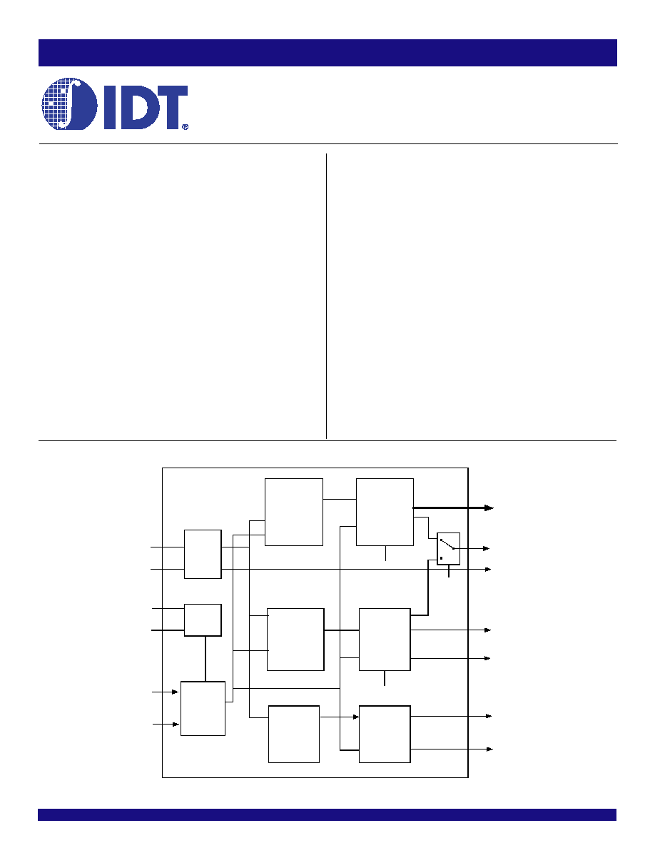
FUNCTIONAL BLOCK DIAGRAM
DESCRIPTION:
IDTCV110J is a 56 pin clock device. The CPU output buffer is designed to
support up to 400MHz processor. This chip has three PLLs inside for CPU/
SRC/PCI, SATA, and 48MHz/DOT96 IO clocks. One dedicated PLL for Serial
ATA clock provides high accuracy frequency. This device also implements
Band-gap referenced I
REF
to reduce the impact of V
DD
variation on differential
outputs, which can provide more robust system performance.
Static PLL frequency divide error can be as low as 36 ppm, worse case 114
ppm, providing high accuracy output clock. Each CPU/SRC/PCI, SATA clock
has its own Spread Spectrum selection, which allows for isolated changes
instead of affecting other clock groups.
OUTPUTS:
∑ 2*0.7V current ≠mode differential CPU CLK pair
∑ 6*0.7V current ≠mode differential SRC CLK pair, one dedicated
for SATA
∑ One CPU_ITP/SRC selectable CLK pair
∑ 9*PCI, 3 free running, 33.3MHz
∑ 1*96MHz, 1*48MHz
∑ 1*REF
KEY SPECIFICATION:
∑ CPU/SRC CLK cycle to cycle jitter < 85ps
∑ SATA CLK cycle to cycle jitter < 85ps
∑ PCI CLK cycle to cycle jitter < 250ps
∑ Static PLL frequency divide error < 114 ppm
∑ Static PLL frequency divide error for 48MHz < 5 ppm

COMMERCIAL TEMPERATURE RANGE
2
IDTCV110J
PROGRAMMABLE FLEXPC CLOCK FOR P4 PROCESSOR
PIN CONFIGURATION
Symbol
Description
Min
Max
Unit
V
DDA
3.3V Core Supply Voltage
4.6
V
V
DDIN
3.3V Logic Input Supply Voltage GND - 0.5
4.6
V
T
STG
Storage Temperature
≠65
+150
∞C
T
AMBIENT
Ambient Operating Temperature
0
+70
∞C
T
CASE
Case Temperature
+115
∞C
ESD Prot
Input ESD Protection
2000
V
Human Body Model
ABSOLUTE MAXIMUM RATINGS
(1)
NOTE:
1. Stresses greater than those listed under ABSOLUTE MAXIMUM RATINGS may cause
permanent damage to the device. This is a stress rating only and functional operation
of the device at these or any other conditions above those indicated in the operational
sections of this specification is not implied. Exposure to absolute maximum rating
conditions for extended periods may affect reliability.
SSOP
TOP VIEW
56
55
54
53
52
51
50
49
48
47
46
45
44
43
42
41
40
39
38
37
36
35
34
33
32
31
30
29
PCI2
PCI1
PCI0
FSC/TEST_SEL
REF
V
SS
_REF
XTAL_IN
XTAL_OUT
V
DD
_REF
SDA
SCL
V
SS
_CPU
CPU0
CPU0#
V
DD
_CPU
CPU1
CPU1#
I
REF
V
SSA
V
DDA
CPU2_ITP/SRC7
CPU2_ITP#/SRC7#
V
DD
_SRC
SRC6#
SRC5
SRC5#
V
SS
_SRC
1
2
3
4
5
6
7
8
9
10
11
12
13
14
15
16
17
18
19
20
21
22
23
24
25
26
27
28
V
DD
_PCI
V
SS
_PCI
PCI3
PCI4
PCI5
V
SS
_PCI
V
DD
_PCI
PCIF
0
/ITP
_
EN
PCIF1
V
TT
_P
WRGD#
/
PD
V
DD
48
USB48
V
SS
48
DOT96
DOT96#
FSB/TEST_MODE
PCIF2
FSA
SRC1
SRC1#
V
DD
_SRC
SRC2
SRC2#
SRC3
SRC3#
SRC4
SRC4#
V
DD
_SRC
SRC6
FREQUENCY SELECTION TABLE
FSC, B, A
CPU
SRC[7:1]
PCI
USB
DOT
REF
101
100
100
33.3
48
96
14.318
001
133
100
33.3
48
96
14.318
011
166
100
33.3
48
96
14.318
010
200
100
33.3
48
96
14.318
000
266
100
33.3
48
96
14.318
100
333
100
33.3
48
96
14.318
110
400
100
33.3
48
96
14.318
111
Reserve
100
33.3
48
96
14.318

COMMERCIAL TEMPERATURE RANGE
IDTCV110J
PROGRAMMABLE FLEXPC CLOCK FOR P4 PROCESSOR
3
PIN DESCRIPTION
Pin Number
Name
Type
Description
1
V
DD
_PCI
PWR
3.3V
2
V
SS
_PCI
GND
GND
3
PCI3
OUT
PCI clock
4
PCI4
OUT
PCI clock
5
PCI5
OUT
PCI clock
6
V
SS
_PCI
GND
GND
7
V
DD
_PCI
PWR
3.3V
8
PCIF0/ITP_EN
I/O
PCI clock, free running. CPU2 select (sampled on V
TT
_P
WRGD
# assertion) HIGH = CPU2.
9
PCIF1
OUT
PCI clock, free running
10
PCIF2
OUT
PCI clock, free running
11
V
DD
48
PWR
3.3V
12
USB48
OUT
48MHz clock
13
V
SS
48
GND
GND
14
DOT96
OUT
96MHz 0.7 current mode differential clock output
15
DOT96#
OUT
96MHz 0.7 current mode differential clock output
16
FSB/TEST_MODE
IN
CPU frequency selection. Selects R
EF
/N or Hi-Z when in test mode, Hi-Z = 1, R
EF
/N = 0.
17
V
TT
_P
WRGD
#/PD
IN
Level-sensitive strobe used to latch the FSA, FSB, FSC/TEST_SEL, and PCIF0/ITP_EN inputs. After
V
TT
_P
WRGD
# assertion, becomes a real-time input for asserting power down. (Active HIGH)
18
FSA
IN
CPU frequency selection
19
SRC1
OUT
Differential serial reference clock
20
SRC1#
OUT
Differential serial reference clock
21
V
DD
_SRC
PWR
3.3V
22
SRC2
OUT
Differential serial reference clock
23
SRC2#
OUT
Differential serial reference clock
24
SRC3
OUT
Differential serial reference clock
25
SRC3#
OUT
Differential serial reference clock
26
SRC4
OUT
Differential serial reference clock
27
SRC4#
OUT
Differential serial reference clock
28
V
DD
_SRC
PWR
3.3V
29
V
SS
_SRC
GND
GND
30
SRC5#
OUT
Differential serial reference clock
31
SRC5
OUT
Differential serial reference clock
32
SRC6#
OUT
Differential serial reference clock
33
SRC6
OUT
Differential serial reference clock
34
V
DD
_SRC
PWR
3.3V
35
CPU2_ITP#/SRC7#
OUT
Selectable CPU or SRC differential clock output. ITP_EN = 0 at V
TT
_P
WRGD
# assertion = SRC7#.
36
CPU2_ITP/SRC7
OUT
Selectable CPU or SRC differential clock output. ITP_EN = 0 at V
TT
_P
WRGD
# assertion = SRC7.
37
V
DDA
PWR
3.3V
38
V
SSA
GND
GND
39
I
REF
OUT
Reference current for differential output buffer
40
CPU1#
OUT
Host 0.7 current mode differential clock output
41
CPU1
OUT
Host 0.7 current mode differential clock output
42
V
DD
_CPU
PWR
3.3V

COMMERCIAL TEMPERATURE RANGE
4
IDTCV110J
PROGRAMMABLE FLEXPC CLOCK FOR P4 PROCESSOR
PIN DESCRIPTION (CONT.)
Pin Number
Name
Type
Description
43
CPU0#
OUT
Host 0.7 current mode differential clock output
44
CPU0
OUT
Host 0.7 current mode differential clock output
45
V
SS
_CPU
GND
GND
46
SCL
IN
SM Bus clock
47
SDA
I/O
SM Bus data
48
V
DD
_REF
PWR
3.3V
49
XTAL_OUT
OUT
XTAL output
50
XTAL_IN
IN
XTAL input
51
V
SS
_REF
GND
GND
52
REF
OUT
14.318 MHz reference clock output
53
FSC/TEST_SEL
IN
CPU frequency selection. Selects test mode if pulled to above 2V when V
TT
_P
WRGD
# is asserted LOW.
54
PCI0
OUT
PCI clock
55
PCI1
OUT
PCI clock
56
PCI2
OUT
PCI clock
INDEX BLOCK WRITE PROTOCOL
Bit
# of bits
From
Description
1
1
Master
Start
2-9
8
Master
D2h
10
1
Slave
Ack (Acknowledge)
11-18
8
Master
Register offset byte (starting byte)
19
1
Slave
Ack (Acknowledge)
20-27
8
Master
Byte count, N (0 is not valid)
28
1
Slave
Ack (Acknowledge)
29-36
8
Master
first data byte (Offset data byte)
37
1
Slave
Ack (Acknowledge)
38-45
8
Master
2nd data byte
46
1
Slave
Ack (Acknowledge)
:
Master
Nth data byte
Slave
Acknowledge
Master
Stop
INDEX BLOCK READ PROTOCOL
Master can stop reading any time by issuing the stop bit without waiting
until Nth byte (byte count bit30-37).
Bit
# of bits
From
Description
1
1
Master
Start
2-9
8
Master
D2h
10
1
Slave
Ack (Acknowledge)
11-18
8
Master
Register offset byte (starting byte)
19
1
Slave
Ack (Acknowledge)
20
1
Master
Repeated Start
21-28
8
Master
D3h
29
1
Slave
Ack (Acknowledge)
30-37
8
Slave
Byte count, N (block read back of N
bytes), power on is 8
38
1
Master
Ack (Acknowledge)
39-46
8
Slave
first data byte (Offset data byte)
47
1
Master
Ack (Acknowledge)
48-55
8
Slave
2nd data byte
Ack (Acknowledge)
:
Master
Ack (Acknowledge)
Slave
Nth data byte
Not acknowledge
Master
Stop
INDEX BYTE WRITE
Setting bit[11:18] = starting address, bit[20:27] = 01h.
INDEX BYTE READ
Setting bit[11:18] = starting address. After reading back the first data byte,
master issues Stop bit.

COMMERCIAL TEMPERATURE RANGE
IDTCV110J
PROGRAMMABLE FLEXPC CLOCK FOR P4 PROCESSOR
5
CONTROL REGISTERS
N PROGRAMMING PROCEDURE
∑
Use Index byte write.
∑
For N programming, the user only needs to access Byte17, Byte 25, and Byte8.
1.
Write Byte17 for CPU PLL N, CPU f = N* Resolution, see resolution table below Byte17.
2.
Write Byte25 for SRC PLL N, SRC f = N*0.666667, PCI = SRC f /3, SATA f = SRC f.
3.
Enable N Programming bit, Byte8 bit1. Once this bit is enabled, any N value will be changed on the fly.
∑
Center spread only works when the N Programming bit is enabled. Down spread is OK even N Programming bit is disabled
∑
It is OK to change N value to any value on the bench test board. In the system, IDT recommends the stepping change. It is unknown how much
the system can sustain for each stepping change; the estimate is about 5. If the N changes too much in one step, the system will likely hang.
∑
Note that SATA is with SRC PLL. This SATA Hard Drive might not operate during SRC N programming.
Most of the Bytes, from Byte8-Byte31, are used to adjust output waveforms and SSC modulation profiles. The power on setting will be changed according
to each power on frequency selection. To avoid mistakes, don't write on those byte (be careful about Block Write). It is suggested to use the Index Byte
write to access bytes.
SSC MAGNITUDE CONTROL, SMC
SMC[2:0]
000
-0.25
001
-0.5
010
-0.75
011
-1
100
±0.125
101
±0.25
110
±0.375
111
±0.5
FS_C, B, A
CPU
101
100
001
133
011
166
010
200
000
266
100
333
110
400
111
RESERVE
FREQUENCY SELECTION TABLE
RESOLUTION
CPU (MHz)
Resolution
N =
100
0.666667
150
133
0.666667
200
166
1.333333
125
200
1.333333
150
266
1.333333
200
333
2.666667
125
400
2.666667
150