 | –≠–ª–µ–∫—Ç—Ä–æ–Ω–Ω—ã–π –∫–æ–º–ø–æ–Ω–µ–Ω—Ç: CY2040-3 | –°–∫–∞—á–∞—Ç—å:  PDF PDF  ZIP ZIP |
32 kHz and 24 MHz Clock Generator with Precision 32 kHz Input
CY2040-2/3
Cypress Semiconductor Corporation
∑
3901 North First Street
∑
San Jose
∑
CA 95134
∑
408-943-2600
Document #: 38-07122 Rev. *A
December 14, 2002
Features
∑ Precision RTC 32 kHz and 24 MHz output
∑ Power-down mode (32 kHz on) is < 50 uA
∑ Suspend mode (V24M = off) is typically 5 uA
∑ Low RMS period Jitter (< 40 ps)
∑ 16-pin TSSOP package
∑ 3.3V + 5% Voltage Supply
∑ CY2040-2 multiplier 32.000 kHz ◊ 750 = 24.0 MHz
(requires a single 32.000 kHz crystal)
∑ CY2040-3 enables the 32 kHz and 24.0 MHz oscillators
(requires a 32.768 kHz and 24.000 MHz crystal)
1
2
3
5
6
7
8
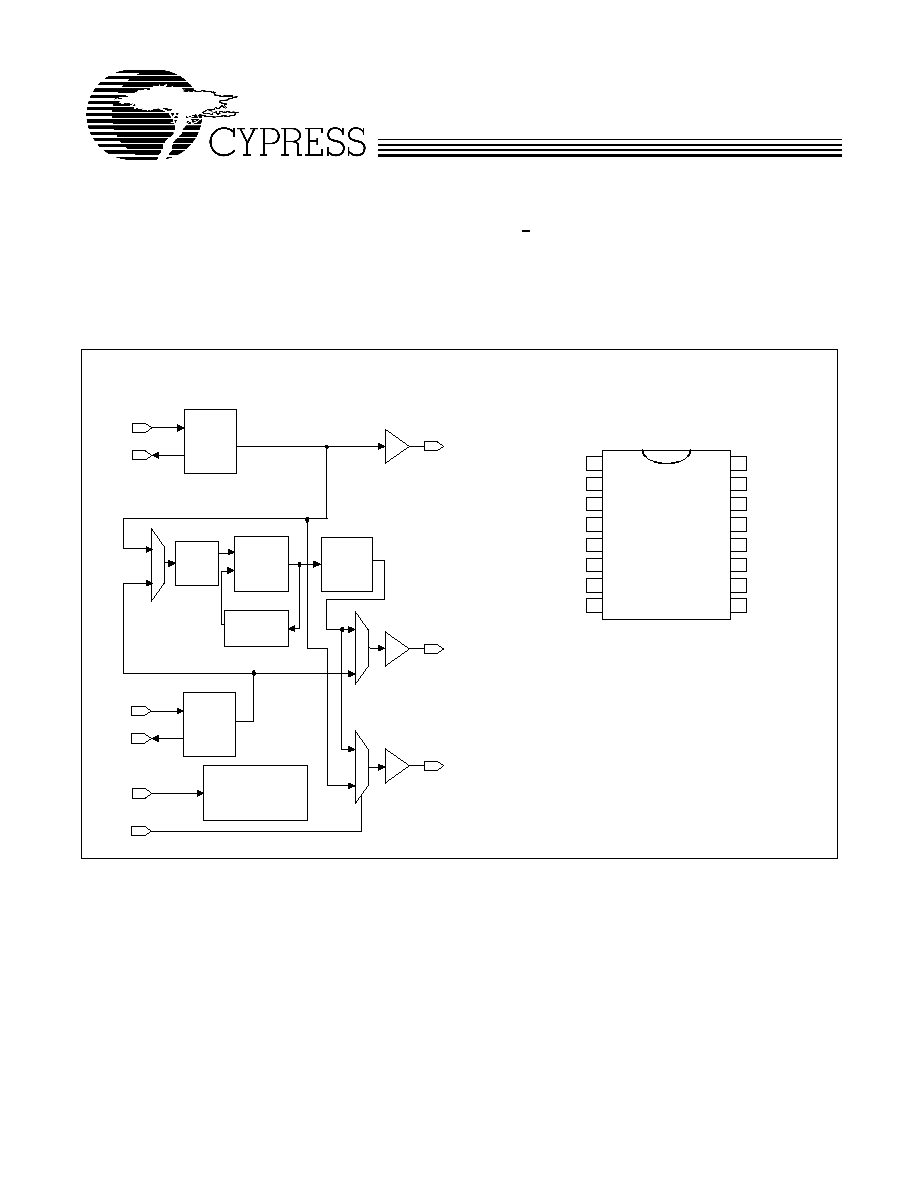
P D 2 4 M #
X IN 3 2 K
X O U T 3 2 K
V 3 2 K
N C
O U T 2 4 M
O U T 3 2 K
3 2 K P L L E N
9
1 6
1 0
1 1
1 2
1 3
1 4
1 5
V S S
V 2 4 M
X IN 2 4 M
X O U T 2 4 M
O U T 3 2 K P L L
V S S
N C
N C
4
Logic Block Diagram
Pin Configuration
XIN32K
XOUT32K
PD24M#
CONTROL LOGIC
32kHz
OSC
24MHz
OSC
Q=INPUT
DIVIDER
PLL
POST
DIVIDER
P=FEEDBACK
DIVIDER
XIN24M
XOUT24M
OUT24M
OUT32K
32KPLLEN
OUT32KPLL
CY2040-2/3
Document #: 38-07122 Rev. *A
Page 2 of 7
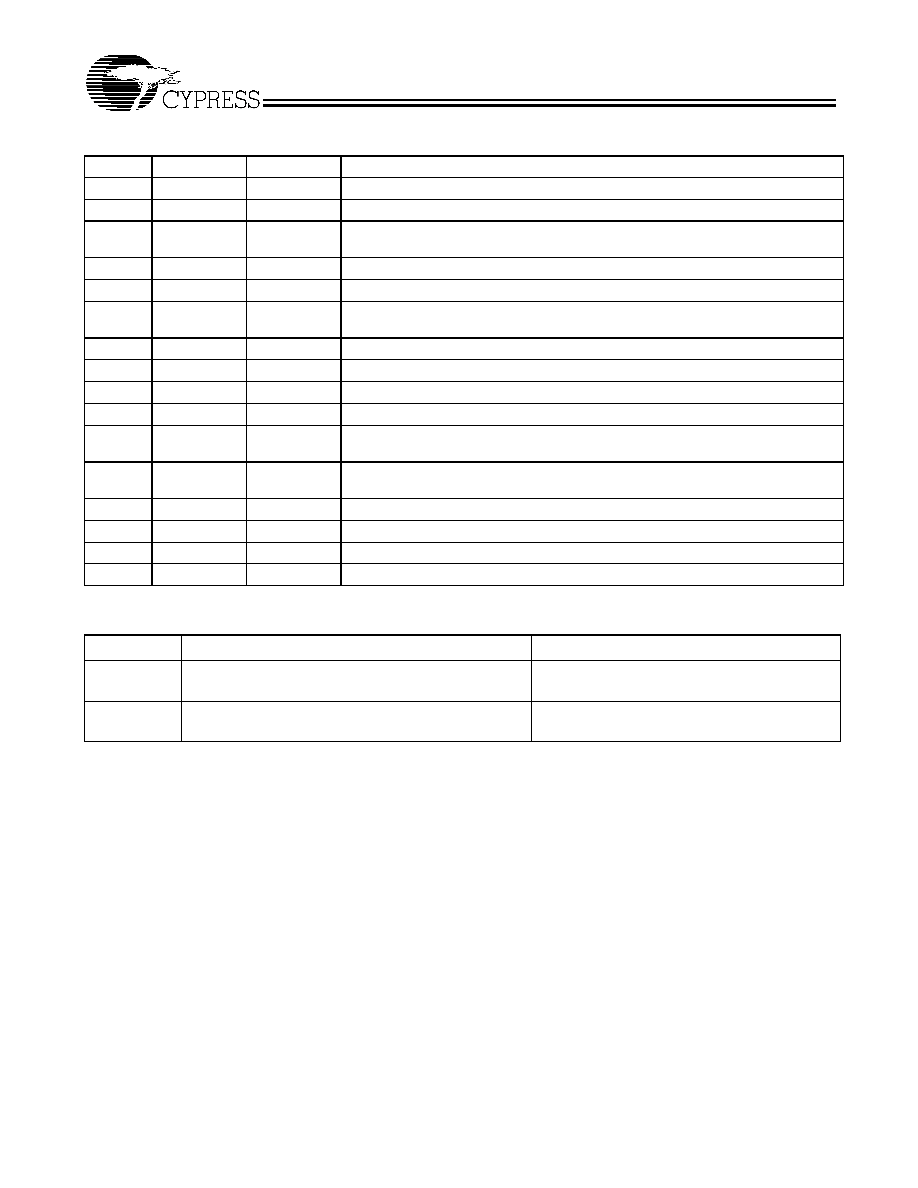
Pin Description
Pin #
Symbol
Type
Description
1
NC
NC
No connection (leave it floating).
2
32KPLLEN
I, PU
OUT32KPLL (pin 14) output enable (OE). 1 = running, 0 = 3-state. Weak pull-up.
3
PD24M#
I, PU
Power down pin to turn off OUT32M, OUT32KPLL, PLL, post divider and 24-MHz
crystal oscillator. Active Low. 1 = running, 0 = power down. Weak pull-up.
4
V32K
[1]
P
3.3V supply for the 32 kHz oscillator circuit (Vbatt).
5
V24M
[1]
P
3.3V supply for the 24 MHz oscillator and PLL circuits (V
DD
).
6
XIN32K
I
Crystal connection input for OSC1.
Recommend using C
Load
= 6 pF crystal with ESR <= 55 k
.
7
XOUT32K
O
Oscillator output pin connected to crystal OSC1.
8
NC
NC
No connection (leave it floating).
9
NC
NC
No connection (leave it floating).
10
VSS
P
Power supply ground.
11
Xin24M
I
Crystal connection input for OSC2. Recommend to use C
Load
= 10pF crystal with
ESR <= 20
. Can be left floating if 24M crystal is not used (CY2040-2).
12
OUT24M
O
Oscillator output pin connected to crystal OSC2. Leave this pin unconnected if 24M
crystal is not used (CY2040-2).
13
OUT32K
O
3.3V 32 kHz buffered output of the reference crystal.
14
OUT32KPLL
O
32 kHz output. Can be enabled/disabled by 32KPLLEN pin.
15
OUT24M
O
3.3V 24 MHz buffered output: either 32 kHz ◊ 750 (-2) or from 24.0 MHz OSC2 (-3).
16
VSS
P
Power supply ground.
Device Configuration
Device
Input Crystals
Output Frequency
CY2040-2
32.000 kHz crystal with C
Load
= 6pF and ESR <= 55 k
.
OUT32K = 32.000 kHz; OUT24M = 24.000 MHz,
OUT32KPLL=32.000kHz
CY2040-3
32.768 kHz crystal with C
Load
= 6pF and ESR <= 55 k
.
24.000 MHz crystal with C
Load
= 10pF and ESR <= 20
.
OUT32K = 32.768 kHz; OUT24M = 24.000 MHz,
OUT32KPLL = 32.768 kHz
Note:
1.
The two power supply pins, V32K and V24M, should be shorted externally.

CY2040-2/3
Document #: 38-07122 Rev. *A
Page 3 of 7
Absolute Maximum Ratings
(Above which the useful life may be impaired. For user guide-
lines, not tested.)
Supply Voltage ................................... ≠0.5V to +7.0V
Input Voltage ...................................... ≠0.5V to V24M +0.5
Storage Temperature
(Non-Condensing) ..............................≠55
∞
C to +150
∞
C
Junction Temperature .........................+150
∞
C
Static Discharge Voltage..................... > 2000V
(per MIL-STD-883, Method 3015)
Operating Conditions
Parameter
Description
Conditions
Min.
Max.
Unit
V32K
Vbatt, Supply voltage
R
elative to V
SS
3.135
3.465
V
V24M
V
DD
, Supply voltage
R
elative to V
SS
3.135
3.465
V
T
A
Operating Temperature, Ambient
Operating Temperature Range, Ambient
0
70
∞
C
C
L
Load Capacitance
Max Capacitive Load on OUT32K,
OUT32KPLL, and OUT24M
15
pF
t
PU
Power-up time for all VDD's to reach
minimum specified voltage (power
ramps must be monotonic)
0.05
50
ms
DC Characteristics
Parameter
Description
Test Conditions
Min.
Typ.
Max.
Unit
V
IL
Input low voltage
(PD24M# and 32KPLLEN
Pins)
V24M = 3.3 + 5%
0.2 V
DD
V
V
IH
Input high voltage
(PD24M# and 32KPLLEN
Pins)
V24M = 3.3 + 5%
0.7 V
DD
V
I
IL
Input low current
(PD24M# and 32KPLLEN
Pins)
V
IN
= 0V
<1
10
µ
A
I
IH
Input high current
(PD24M# and 32KPLLEN
Pins)
V
IN
=
V24M
<1
5
µ
A
I
DD
Dynamic Supply Current with
no load at outputs.
V24M
= V32K = 3.3 + 5%,
f
OUT32K
= 32.768kHz or 32.000kHz,
f
OUT24M
= 24MHz, f
OUT32KPLL
= 3-state.
10
25
mA
I
PT
Power-down Supply Current V24M
= V32K = 3.3 + 5%
(PD24M# = "0")
20
50
µ
A
OUT32K (V32K = 3.3V +5%)
V
OL
Output low voltage
V32K
= 3.3 + 5%,
I
OL
= 8 mA
0.4
V
V
OH
Output high voltage
V32K
= 3.3 + 5%,
I
OH
= ≠ 8 mA
V32K ≠ 0.4
OUT24M (V24M = 3.3V +5%)
V
OL
Output low voltage
V24M
= 3.3 + 5%,
I
OL
= 8 mA
0.4
V
V
OH
Output high voltage
V24M
= 3.3 + 5%,
I
OH
= ≠ 8 mA
V24M ≠ 0.4
I
OZ
Output leakage current
(OUT24M)
V24M
= 3.3 + 5%,
with output disabled
1
50
µ
A
OUT32KPLL (V24M = 3.3V +5%)
V
OL
Output low voltage
V24M
= 3.3 + 5%,
I
OL
= 8 mA
0.4
V
V
OH
Output high voltage
V24M
= 3.3 + 5%,
I
OH
= ≠8 mA
V24M ≠ 0.4

CY2040-2/3
Document #: 38-07122 Rev. *A
Page 4 of 7
I
OZ
Output leakage current
(OUT32KPLL)
V24M
= 3.3 + 5%,
with output disabled
1
50
µ
A
DC Characteristics
Parameter
Description
Test Conditions
Min.
Typ.
Max.
Unit
AC Characteristics
Parameter
Description
Test Conditions
Min.
Typ.
Max.
Unit
OUT32K AC Characteristics
tr1
OUT32K Rise time
20% to 80% V32K
7.0
ns
tf1
OUT32K Fall time
80% to 20% V32K
7.0
ns
dc1
OUT32K Duty Cycle
C
LT
= 15 pF, measured at V32K/2
40
60
%
tj1
Pk-Pk Period jitter
32.000 kHz output directly from oscillator (with
crystal), measured at V32K/2
20
40
ns
OUT24M AC Characteristics
tr2
OUT24M Rise Time
V24M
= 3.3 + 5%; 20% to 80% V24M
4.0
ns
tf2
OUT24M Fall Time
V24M
= 3.3 + 5%; 80% to 20% V24M
4.0
ns
dc2
OUT24M Duty cycle
V24M
= 3.3 + 5%;
measured at V24M/2
40
60
%
tj2
RMS Period Jitter
(CY2040-2, PLL output)
V24M = V32K =
3.3 + 5%; 32 kHz as input to PLL;
measured at V24M/2
40
ps
RMS Period Jitter
(CY2040-3, osc. output)
V24M = V32K =
3.3 + 5%;
24 MHz output directly
from oscillator; measured at V24M/2
40
ps
tj3
RMS Long-term Jitter
(CY2040-2, PLL output)
V24M = V32K =
3.3 + 5%; 32 kHz as input to PLL;
measured at V24M/2 on the 750th output rising
edge.
1.5
ns
OUT32KPLL AC Characteristics
tr3
OUT32KPLL Rise Time
V24M
= 3.3 + 5%; 20% to 80% V24M
7.0
ns
tf3
OUT32KPLL Fall Time
V24M
= 3.3 + 5%; 80% to 20% V24M
7.0
ns
dc3
OUT32KPLL Duty cycle
V24M
= 3.3 + 5%;
measured at V24M/2
40
60
%
tj4
Pk-Pk Period Jitter
(32 kHz osc. output)
32.000 kHz output directly from oscillator, mea-
sured at V24M/2
20
40
ns
Other AC Characteristics
t
start
Osc start up time
From power on (V32K =
3.3 + 5%
). Decided by
32.768 kHz/32.000 kHz crystal startup.
3
sec
t
PD
Power down delay time on
OUT24M; SYNC
PD24M# pin high to low
(T = OUT24M clock period)
T/2
T+25
ns
t
PU
Power up time on OUT24M;
ASYNC (CY2040-2)
From power down mode; PD24M# pin low to
high.
1
5
ms
Power up time on OUT24M;
ASYNC (CY2040-3)
From power down mode; PD24M# pin low to
high. Decided by 24 MHz crystal start-up.
6
10
ms
CY2040-2/3
Document #: 38-07122 Rev. *A
Page 5 of 7
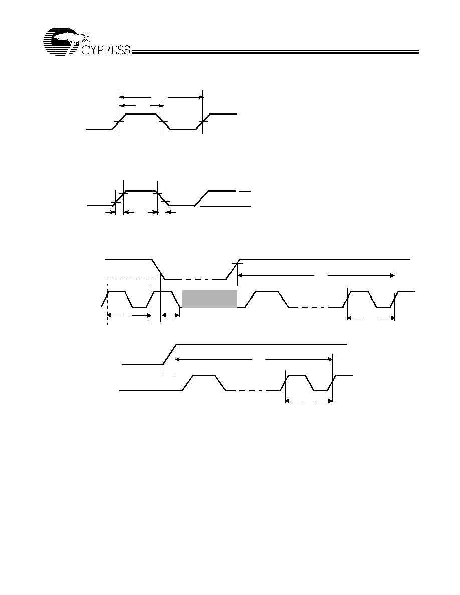
Switching Waveforms
Duty Cycle Timing (dc1, dc2, dc3)
t
1A
t
1B
OUTPUT
Output Rise/Fall Time
OUTPUT
t
r
V
DD
0V
t
f
Power Down and Power up Timing (synchronous modes)
CLKOUT
V
DD
t
PU
1/f
t
PD
V
IL
V
IH
POWER
DOWN/UP
0V
T
(synchronous)
High Impedance
Crystal Start-up Timing
CLKOUT
V
DD
t
start
1/f
V
DD
≠ 10%
CRYSTAL
0V
min. 30us
START-UP
max. 30ms