 | –≠–ª–µ–∫—Ç—Ä–æ–Ω–Ω—ã–π –∫–æ–º–ø–æ–Ω–µ–Ω—Ç: CY2071AF | –°–∫–∞—á–∞—Ç—å:  PDF PDF  ZIP ZIP |

CY2071A
Single-PLL General-Purpose
EPROM Programmable Clock Generator
Cypress Semiconductor Corporation
∑
3901 North First Street
∑
San Jose
∑
CA 95134
∑
408-943-2600
Document #: 38-07139 Rev. *A
Revised December 14, 2002
i
Features
Benefits
Single phase-locked loop architecture
Generates a custom frequency from an external source
EPROM programmability
Easy customization and fast turnaround
Factory-programmable (CY2071A, CY2071AI) or field-
programmable (CY2071AF, CY2071AFI) device options
Programming support available for all opportunities
Up to three configurable outputs
Generates three related frequencies from a single device
Low-skew, low-jitter, high-accuracy outputs
Meets critical industry standard timing requirements
Internal loop filter
Alleviates the need for external components
Power management (OE)
Supports low-power applications
Frequency select options
3 outputs with 2 user selectable frequencies
Configurable 5V or 3.3V operation
Supports industry standard design platforms
8-pin 150-mil SOIC package
Industry-standard packaging saves on board space
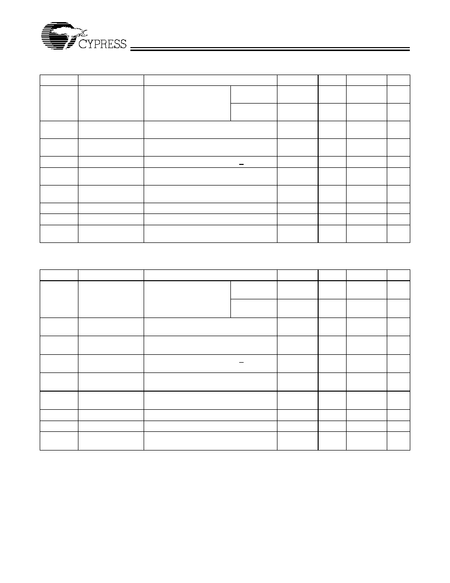
Selector Guide
Part Number
Outputs
Input Frequency Range
Output Frequency Range
Specifics
CY2071A
3
10 MHz≠25 MHz (external crystal)
1 MHz≠30 MHz (reference clock)
500 kHz≠130 MHz (5V)
500 kHz≠100 MHz (3.3V)
Factory Programmable
Commercial Temperature
CY2071AI
3
10 MHz≠25 MHz (external crystal)
1 MHz≠30 MHz (reference clock)
500 kHz≠100 MHz (5V)
500 kHz≠80 MHz (3.3V)
Factory Programmable
Industrial Temperature
CY2071AF
3
10 MHz≠25 MHz (external crystal)
1 MHz≠30 MHz (reference clock)
500 kHz≠100 MHz (5V)
500 kHz≠80 MHz (3.3V)
Field Programmable
Commercial Temperature
CY2071AFI
3
10 MHz≠25 MHz (external crystal)
1 MHz≠30 MHz (reference clock)
500 kHz≠90 MHz (5V)
500 kHz≠66.6 MHz (3.3V)
Field Programmable
Industrial Temperature
1
2
3
4
5
8
7
6
CLKA
GND
XTALIN
XTALOUT
VDD
OE/FS
CLKC
CLKB
XTALOUT
XTALIN
REFERENCE
OSCILLATOR
PLL
Block
CLKA
CLKB
CLKC
EPROM-
Configurable
Multiplexer
and Divide
Logic
OE / FS
Logic Block Diagram for CY2071A
Top View
8-pin SOIC
Pin Configuration

CY2071A
Document #: 38-07139 Rev. *A
Page 2 of 8
Functional Description
The CY2071A is a general-purpose clock synthesizer de-
signed for use in applications such as modems, disk drives,
CD-ROM drives, video CD players, games, set-top boxes, and
data/telecommunications. The device offers up to three con-
figurable clock outputs in an 8-pin, 150-mil SOIC package and
can operate off either a 3.3V or 5V power supply. The on-chip
reference oscillator is designed for 10-MHz to 25-MHz crys-
tals. Alternatively, an external reference clock of frequency be-
tween 1 MHz and 30 MHz can be used.
The CY2071A has one PLL and outputs three factory-EPROM
configurable clocks: CLKA, CLKB, and CLKC. The output
clocks can originate either from the PLL or the reference, or
selected dividers thereof. Additionally, pin 8 can be configured
to be an Output Enable or a Select input.
The CY2071A can replace multiple Metal Can Oscillators
(MCO) in a synchronous system, providing cost and board
space savings to the manufacturer. Hence, these devices are
ideally suited for applications that require multiple, accurate,
and stable clocks synthesized from low-cost generators in
small packages. A hard-disk drive is an example of such an
application. In this case, CLKA drives the PLL in the Read
Controller, while CLKB and CLKC drive the MCU and associ-
ated sequencers.
CyClocksTM Software
CyClocks is an easy-to-use software application that allows
you to configure any one of the EPROM-Programmable
Clocks offered by Cypress. You may specify the input frequen-
cy, PLL and output frequencies, and different functional op-
tions. Please note the output frequency ranges in this data
sheet when specifying them in CyClocks to ensure that you
stay within the limits. You can download a copy of CyClocks
free on the Cypress Semiconductor website at www.cy-
press.com.
Consider using the CY2081 for applications that require unre-
lated output frequencies. Consider using the CY2291,
CY2292, or CY2907 for applications that require more than
three output clocks.
Cypress FTG Programmer
The Cypress Frequency Timing Generator (FTG) Programmer
is a portable programmer designed to custom program our
family of EPROM Field Programmable Clock Devices. The
FTG programmers connect to a PC serial port and allow users
of CyClocks software to quickly and easily program any of the
CY2291F, CY2292F, CY2071AF, and CY2907F devices. The
ordering code for the Cypress FTG Programmer is CY3670.
Maximum Ratings
(Above which the useful life may be impaired. For user guide-
lines, not tested.)
Supply Voltage ...............................................≠0.5V to +7.0V
DC Input Voltage ..................................... ≠0.5V to V
DD
+0.5V
Storage Temperature ................................. ≠65∞C to +150∞C
Max. Soldering Temperature (10 sec) ..........................260∞C
Junction Temperature ...................................................150∞C
Static Discharge Voltage............................................ >2000V
(per MIL-STD-883, Method 3015)
Pin Summary
Name
Number
Description
CLKA
1
Configurable Clock Output
GND
2
Ground
XTALIN
[1]
3
Reference Crystal Input or External Reference Clock Input
XTALOUT
[1, 2]
4
Reference Crystal Feedback
CLKB
5
Configurable Clock Output
CLKC
6
Configurable Clock Output
V
DD
7
Voltage Supply
OE / FS
8
Output Control Pin, either Output Enable or Frequency Select Input
(Active-HIGH, internal pull-up resistor to V
DD
)
Notes:
1.
For best accuracy, use a parallel-resonant crystal, C
L
= 17 pF.
2.
Float XTALOUT pin if XTALIN is driven by reference clock (as opposed to an external crystal).

CY2071A
Document #: 38-07139 Rev. *A
Page 3 of 8
Operating Conditions
[3]
Parameter
Description
Min.
Max.
Unit
V
DD
Supply Voltage, 5.0V Operation
4.5
5.5
V
V
DD
Supply Voltage, 3.3V Operation
3.0
3.6
V
T
A
Commercial Operating Temperature, Ambient
0
70
∞C
Industrial Operating Temperature, Ambient
≠40
85
∞C
C
L
Max. Load Capacitance per Output (5V Operation)
25
pF
Max. Load Capacitance per Output (3.3V Operation)
15
pF
f
REF
External Reference Crystal
10.0
25.0
MHz
External Reference Clock
[4, 5]
1.0
30.0
MHz
t
PU
Power-up time for all VDD's to reach minimum specified voltage (power
ramps must be monotonic)
0.05
50
ms
Electrical Characteristics, Commercial 5.0V
V
DD
= 5V ±10%, T
A
= 0
∞
C to +70
∞
C
Parameter
Description
Conditions
Min.
Typ.
Max.
Unit
V
OH
HIGH-Level Output Voltage
I
OH
= ≠4.0 mA
2.4
V
V
OL
LOW-Level Output Voltage
I
OL
= 4.0 mA
0.4
V
V
IH
HIGH-Level Input Voltage
[6]
Except Crystal Pins
2.0
V
V
IL
LOW-Level Output Voltage
[6]
Except Crystal Pins
0.8
V
I
IH
Input HIGH Current
V
IN
= V
DD
≠ 0.5V
10
µ
A
I
IL
Input LOW Current
V
IN
= 0.5V
150
µ
A
I
OZ
Output Leakage Current
Three State Outputs
250
µ
A
I
DD
V
DD
Supply Current
[7]
V
DD
= V
DD
max. 5V operation, C
L
= 25 pF
40
60
mA
Electrical Characteristics, Commercial 3.3V
V
DD
= 3.3V ±10%, T
A
= 0
∞
C to +70
∞
C
Parameter
Description
Conditions
Min.
Typ.
Max.
Unit
V
OH
HIGH-Level Output Voltage
I
OH
= ≠4.0 mA
2.4
V
V
OL
LOW-Level Output Voltage
I
OL
= 4.0 mA
0.4
V
V
IH
HIGH-Level Input Voltage
[6]
Except Crystal Pins
2.0
V
V
IL
LOW-Level Output Voltage
[6]
Except Crystal Pins
0.8
V
I
IH
Input HIGH Current
V
IN
= V
DD
≠ 0.5V
10
µ
A
I
IL
Input LOW Current
V
IN
= 0.5V
150
µ
A
I
OZ
Output Leakage Current
Three State Outputs
250
µ
A
I
DD
V
DD
Supply Current
[7]
V
DD
= V
DD
max. 3.3V operation,
C
L
=
15 pF
24
40
mA
Notes:
3.
Electrical parameters are guaranteed with these operating conditions. Values for 3.3V operation are shown in parentheses.
4.
External input reference clock must have a duty cycle between 40% and 60%, measured at V
DD
/2.
5.
Please refer to application note "Crystal Oscillator Topics" for information on AC-coupling the external input reference clock.
6.
Xtal inputs have CMOS thresholds.
7.
Load = max, typical configuration, f
REF
= 14.318 MHz. Specific configurations may vary. A close approximation of I
DD
can be derived by the following formula:
I
DD
(mA) = V
DD
*(6.25+(0.055*F
REF
) + (0.0017*C
LOAD
*(F
CLKA
+F
CLKB
+F
CLKC
))). C
LOAD
is specified in pF and F is specified in MHz.

CY2071A
Document #: 38-07139 Rev. *A
Page 4 of 8
Electrical Characteristics, Industrial 5.0V
V
DD
=5.0V ±10%, T
A
= ≠40∞C to +85∞C
Parameter
Description
Conditions
Min.
Typ.
Max.
Unit
V
OH
HIGH-Level Output Voltage
I
OH
= ≠4.0 mA
2.4
V
V
OL
LOW-Level Output Voltage
I
OL
= 4.0 mA
0.4
V
V
IH
HIGH-Level Input Voltage
[6]
Except Crystal Pins
2.0
V
V
IL
LOW-Level Output Voltage
[6]
Except Crystal Pins
0.8
V
I
IH
Input HIGH Current
V
IN
= V
DD
≠ 0.5V
10
µ
A
I
IL
Input LOW Current
V
IN
= 0.5V
150
µ
A
I
OZ
Output Leakage Current
Three State Outputs
250
µ
A
I
DD
V
DD
Supply Current
[7]
V
DD
= V
DD
max. 5V operation, C
L
= 25 pF
40
75
mA
Electrical Characteristics, Industrial 3.3V
V
DD
=3.3V ±10%, T
A
= ≠40∞C to +85∞C
Parameter
Description
Conditions
Min.
Typ.
Max.
Unit
V
OH
HIGH-Level Output Voltage
I
OH
= ≠4.0 mA
2.4
V
V
OL
LOW-Level Output Voltage
I
OL
= 4.0 mA
0.4
V
V
IH
HIGH-Level Input Voltage
[6]
Except Crystal Pins
2.0
V
V
IL
LOW-Level Output Voltage
[6]
Except Crystal Pins
0.8
V
I
IH
Input HIGH Current
V
IN
= V
DD
≠ 0.5V
10
µ
A
I
IL
Input LOW Current
V
IN
= 0.5V
150
µ
A
I
OZ
Output Leakage Current
Three State Outputs
250
µ
A
I
DD
V
DD
Supply Current
[7]
V
DD
= V
DD
max. 3.3V operation,
C
L
=
15 pF
24
50
mA
Switching Characteristics, Commercial 5.0V
[8]
Parameter
Name
Description
Min.
Typ.
Max.
Unit
t
1
Output Period
Clock output range
5V operation
25-pF load
CY2071A
7.692
[130 MHz]
2000
[500 kHz]
ns
CY2071AF
10
[100 MHz]
2000
[500 kHz]
ns
t
1A
Clock Jitter
Peak-to-peak period jitter (t
1
max. ≠ t
1
min.),
% of clock period, f
OUT
16 MHz
0.8
1
%
t
1B
Clock Jitter
Peak-to-peak period jitter
(16 MHz
f
OUT
50 MHz)
350
500
ps
t
1C
Clock Jitter
[9]
Peak-to-peak period jitter (f
OUT
> 50 MHz)
250
350
ps
Output Duty Cycle
Duty cycle
[10, 11]
for outputs, (t
2
˜
t
1
)
f
OUT
60 MHz
45%
50%
55%
Output Duty Cycle
[9]
Duty cycle
[11]
for outputs, (t
2
˜
t
1
),
f
OUT
> 60 MHz
40%
50%
60%
t
3
Rise Time
[9]
Output clock rise time
1.5
2.5
ns
t
4
Fall Time
[9]
Output clock fall time
1.5
2.5
ns
t
5
Skew
Skew delay between any two outputs with
identical frequencies (generated by the PLL)
0.5
ns
Notes:
8.
Guaranteed by design, not 100% tested.
9.
When the output clock frequency is between 100 MHz and 130 MHz at 5V, the maximum capacitive load for these measurements is 15 pF.
10. Reference Output duty cycle depends on XTALIN duty cycle.
11.
Measured at 1.4V.
CY2071A
Document #: 38-07139 Rev. *A
Page 5 of 8
Switching Characteristics, Commercial 3.3V
[8]
Parameter
Name
Description
Min.
Typ.
Max.
Unit
t
1
Output Period
Clock output range
3.3V operation
15-pF load
CY2071AS
10
[100 MHz]
2000
[500 kHz]
ns
CY2071AF
12.50
[80 MHz]
2000
[500 kHz]
ns
t
1A
Clock Jitter
Peak-to-peak period jitter (t
1
max. ≠ t
1
min.),
% of clock period, f
OUT
16 MHz
0.8
1
%
t
1B
Clock Jitter
Peak-to-peak period jitter
(16 MHz
f
OUT
50 MHz)
350
500
ps
t
1C
Clock Jitter
[9]
Peak-to-peak period jitter (f
OUT
> 50 MHz)
250
350
ps
Output Duty Cycle
Duty cycle
[10, 11]
for outputs, (t
2
˜
t
1
)
f
OUT
60 MHz
45%
50%
55%
Output Duty Cycle
[9]
Duty cycle
[11]
for outputs, (t
2
˜
t
1
),
f
OUT
> 60 MHz
40%
50%
60%
t
3
Rise Time
[9]
Output clock rise time
1.5
2.5
ns
t
4
Fall Time
[9]
Output clock fall time
1.5
2.5
ns
t
5
Skew
Skew delay between any two outputs with
identical frequencies (generated by the PLL)
0.5
ns
Switching Characteristics, Industrial 5.0V
[8]
Parameter
Name
Description
Min.
Typ.
Max.
Unit
t
1
Output Period
Clock output range
5.0V operation
25-pF load
CY2071AI
10
[100 MHz]
2000
[500 kHz]
ns
CY2071AFI
11.1
[90 MHz]
2000
[500 kHz]
ns
t
1A
Clock Jitter
Peak-to-peak period jitter (t
1
max. ≠ t
1
min.),
% of clock period, f
OUT
16 MHz
0.8
1
%
t
1B
Clock Jitter
Peak-to-peak period jitter
(16 MHz
f
OUT
50 MHz)
350
500
ps
t
1C
Clock Jitter
[9]
Peak-to-peak period jitter (f
OUT
> 50 MHz)
250
350
ps
Output Duty Cycle
Duty cycle
[10, 11]
for outputs, (t
2
˜
t
1
)
f
OUT
60 MHz
45%
50%
55%
Output Duty Cycle
[9]
Duty cycle
[11]
for outputs, (t
2
˜
t
1
),
f
OUT
>
60 MHz
40%
50%
60%
t
3
Rise time
[9]
Output clock rise time
1.5
2.5
ns
t
4
Fall time
[9]
Output clock fall time
1.5
2.5
ns
t
5
Skew
Skew delay between any two outputs with
identical frequencies (generated by the PLL)
0.5
ns