 | –≠–ª–µ–∫—Ç—Ä–æ–Ω–Ω—ã–π –∫–æ–º–ø–æ–Ω–µ–Ω—Ç: CY2254A-1 | –°–∫–∞—á–∞—Ç—å:  PDF PDF  ZIP ZIP |

Pentium
Æ
Processor Compatible
Clock Synthesizer/Driver
CY2254A
Cypress Semiconductor Corporation
∑
3901 North First Street
∑
San Jose
∑
CA 95134
∑
408-943-2600
Document #: 38-07203 Rev. *A
Revised December 14, 2002
4A
Features
∑ Multiple clock outputs to meet requirements of most
Pentium
Æ
motherboards
-- Four pin-selectable CPU clocks @ 66.66 MHz, 60.0
MHz, and 50.0 MHz for support of Intel Triton
TM
PCIset
based PC
-- 55.0 MHz pin-selectable CPU clock also available (
-
2
option only)
-- Six PCI clocks at 1/2 CPU Clock frequency
-- One I/O clock @ 24 MHz
-- One Keyboard Controller clock @ 12 MHz (
-
1 option)
or one Universal Serial Bus clock @ 48 MHz
(
-
2 option)
-- Two Ref. clocks @ 14.318 MHz
-- Ref. 14.318 MHz Xtal oscillator input
∑ CPU clock jitter < 200 ps cycle-to-cycle
∑ Low skew outputs
-- < 250 ps between CPU clocks
-- < 250 ps between PCI clocks
-- < 500 ps between CPU and PCI clocks (
-
2 option)
-- CPU clock leads PCI clock by +1 ns min. to +4 ns
max. (
-
1 option)
∑ Freq. stability = 0.01% (max.)
∑ Output duty cycle 45% min. to 55% max.
∑ Test mode support (
-
1 option only)
∑ 3.3V or 5.0V operation
∑ Internal pull-up resistors on S0, S1, and OE inputs
Functional Description
The CY2254A is a Clock Synthesizer/Driver that provides the
multiple clocks required for a Pentium-based PC. The
CY2254A has low-skew outputs (< 250 ps between the CPU
Clocks, < 250 ps between the PCI Clocks). In addition, the
CY2254A CPU clock outputs have less than 200 ps cy-
cle-to-cycle jitter. Finally, both the PCI and CPU clock outputs
meet the 1 V/ns slew rate requirement of a Pentium proces-
sor-based system.
The CY2254A accepts a 14.318 MHz reference signal as its
input. The CY2254A has 2 PLLs, one of which generates the
CPU and PCI clocks, and the other generates the I/O and Key-
board Controller or USB clocks. The CY2254A runs off either
a 3.3V or 5V supply.
The CY2254A is available in two options. The
-
1 option sup-
ports the Intel Triton PCIset and provides a 12 MHz keyboard
clock on pin 25. The
-
2 option provides a 48 MHz USB clock
on pin 25 and supports the Cyrix
Æ
M1 processor.
Intel and Pentium are registered trademarks of Intel Corporation.
Triton is a trademark of Intel Corporation.
Cyrix is a registered trademark of Cyrix Corporation.
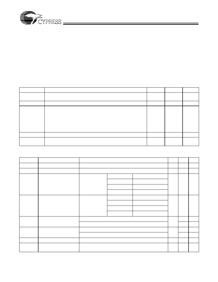
Pin Configuration
Logic Block Diagram
XTALOUT
XTALIN
REF0 (14.318 MHz)
14.318
MHz
OSC.
1
2
3
4
5
6
7
8
9
10
11
12
15
16
17
18
19
20
24
23
22
21
13
14
25
28
27
26
Top View
V
DD
XTALIN
XTALOUT
V
SS
OE
CPUCLK0
CPUCLK1
V
DD
CPUCLK2
CPUCLK3
V
SS
S1
S0
V
DD
REF0
REF1
V
DD
SEEBELOW
IOCLK
V
SS
PCICLK2
PCICLK3
V
DD
PCICLK4
PCICLK5
V
SS
PCICLK1
PCICLK0
REF1 (14.318 MHz)
IOCLK (24 MHz)
CPUCLK0
CPUCLK1
CPUCLK2
CPUCLK3
PCICLK0
SYS
PLL
CPU
PLL
ROM
S0
S1
OE
˜
2
DELAY
PCICLK1
PCICLK2
PCICLK3
PCICLK4
PCICLK5
SOIC
USBCLK (48 MHz)
KBDCLK (12 MHz)
˜
2
˜
2
-
1
-
2
OPTION
PIN 25
KBDCLK
12 MHz
USBCLK
48 MHz
-
1 option only

CY2254A
Document #: 38-07203 Rev. *A
Page 2 of 8
Pin Summary
Name
-
1
-
2
Description
V
DD
1
1
Voltage supply
XTALIN
[1]
2
2
Reference crystal input
XTALOUT
[1]
3
3
Reference crystal feedback
V
SS
4
4
Ground
OE
5
5
Output Enable, Active HIGH (internal pull-up resistor to V
DD
)
CPUCLK0
6
6
CPU clock output
CPUCLK1
7
7
CPU clock output
V
DD
8
8
Voltage supply
CPUCLK2
9
9
CPU clock output
CPUCLK3
10
10
CPU clock output
V
SS
11
11
Ground
S1
12
12
CPU clock select input, bit 1 (internal pull-up resistor to V
DD
)
S0
13
13
CPU clock select input, bit 0 (internal pull-up resistor to V
DD
)
V
DD
14
14
Voltage supply
PCICLK0
15
15
PCI clock output
PCICLK1
16
16
PCI clock output
V
SS
17
17
Ground
PCICLK5
18
18
PCI clock output
PCICLK4
19
19
PCI clock output
V
DD
20
20
Voltage supply
PCICLK3
21
21
PCI clock output
PCICLK2
22
22
PCI clock output
V
SS
23
23
Ground
IOCLK
24
24
I/O clock output (24 MHz)
KBDCLK
25
Keyboard controller clock output (12 MHz)
USBCLK
25
Universal Serial Bus clock output (48 MHz)
V
DD
26
26
Voltage supply
REF1
27
27
Reference clock output (14.318 MHz)
REF0
28
28
Reference clock output (14.318 MHz)
Function Table
Option
OE
S0
S1
XTALIN
CPUCLK
PCICLK
Ref. Clock
Output
IOCLK
KBDCLK
-
1 only
USBCLK
-
2 only
-
1,
-
2
0
X
X
14.318 MHz High-Z
High-Z
High-Z
High-Z
High-Z
High-Z
-
1,
-
2
1
0
0
14.318 MHz 50.0 MHz
25.0 MHz
14.318 MHz 24 MHz
12 MHz
48 MHz
-
1,
-
2
1
0
1
14.318 MHz 60.0 MHz
30.0 MHz
14.318 MHz 24 MHz
12 MHz
48 MHz
-
1,
-
2
1
1
0
14.318 MHz 66.66 MHz
33.33 MHz
14.318 MHz 24 MHz
12 MHz
48 MHz
-
1
1
1
1
TCLK
[2]
TCLK/2
TCLK/4
TCLK
TCLK/4
TCLK/8
-
2
1
1
1
14.318 MHz 55.0 MHz
27.5 MHz
14.318 MHz 24 MHz
48 MHz
Notes:
1.
For best accuracy, use a parallel-resonant crystal, C
LOAD
= 17 pF.
2.
TCLK is a test clock on XTALIN (pin 2) during test mode.
CY2254A
Document #: 38-07203 Rev. *A
Page 3 of 8
PCI Clock Driver Strength Requirements
∑ Matched impedances on both rising and falling edges on
the output drivers
∑ Output impedance: 25
(typical) measured at 1.5V
∑ Maximum output impedance: 40
measured at 1.5V
CPU Clock Driver Strength Requirements
∑ Matched impedances on both rising and falling edges on
the output drivers
∑ Output impedance: 25
(typical) measured at 1.5V
∑ Maximum output impedance: 40
measured at 1.5V
Maximum Ratings
(Above which the useful life may be impaired. For user guide-
lines, not tested.)
Supply Voltage
........................................................-
0.5 to +7.0V
Input Voltage
................................................. -
0.5V to V
DD
+ 0.5
Storage Temperature (Non-Condensing)
.... -
65
∞
C to +150
∞
C
Junction Temperature ............................................... +150
∞
C
Package Power Dissipation.............................................. 1W
Static Discharge Voltage............................................ >2000V
(per MIL-STD-883, Method 3015)
Operating Conditions
[3]
Parameter
Description
Min.
Max.
Unit
V
DD
Supply Voltage 3.3V
Supply Voltage 5.0V
3.135
4.5
3.6
5.5
V
V
T
A
Operating Ambient Temperature
0
70
∞
C
C
L
Max. Capacitive Load on
CPUCLK
PCICLK
IOCLK
KBDCLK / USBCLK
REF0
REF1
20
30
20
20
30
15
pF
f
(REF)
Reference Frequency, Oscillator Nominal Value
14.318
14.318
MHz
t
PU
Power-up time for all VDD's to reach minimum specified voltage (power
ramps must be monotonic)
0.05
50
ms
Electrical Characteristics
V
DD
= 3.135V
-
3.6V, or 5.0V
±
10%, T
A
= 0
∞
C to +70
∞
C
Parameter
Description
Test Conditions
Min.
Max.
Unit
V
IH
High-level Input Voltage
Except Crystal Inputs
2.0
V
V
IL
Low-level Input Voltage
Except Crystal Inputs
0.8
V
V
OH
[4]
High-level Output Voltage
V
DD
= V
DD
Min.
I
OH
= 6 mA
CPUCLK
2.4
V
I
OH
= 12 mA
PCICLK, REF0
I
OH
= 4 mA
KBDCLK, USBCLK
I
OH
= 8 mA
REF1
V
OL
[4]
Low-level Output Voltage
V
DD
= V
DD
Min.
I
OL
= 6 mA
CPUCLK
0.4
V
I
OL
= 12 mA
PCICLK, REF0
I
OL
= 4 mA
KBDCLK, USBCLK
I
OL
= 8 mA
REF1
I
IH
Input High Current
V
IH
= V
DD,
V
DD
= 3.3V
5
µ
A
V
IH
= V
DD,
V
DD
= 5.0V
10
µ
A
I
IL
Input Low Current
V
IL
= 0 V, V
DD
= 3.3V
100
µ
A
V
IL
= 0 V, V
DD
= 5.0V
250
µ
A
I
OZ
Output Leakage Current
Three-state
-
10
+10
µ
A
I
DD
Power Supply Current
V
DD
= 3.6V, V
IN
= 0 or V
DD
V
DD
= 5.5V, V
IN
= 0 or V
DD
90
150
mA
mA
CY2254A
Document #: 38-07203 Rev. *A
Page 4 of 8
Notes:
3.
Electrical parameters are guaranteed with these operating conditions.
4.
Guaranteed by design, not tested.
Electrical Characteristics
V
DD
= 3.135V
-
3.6V, or 5.0V
±
10%, T
A
= 0
∞
C to +70
∞
C (continued)
Parameter
Description
Test Conditions
Min.
Max.
Unit
Switching Characteristics
[5]
Parameter
Output
Name
Description
Min.
Max.
Unit
t
1
All
Output Duty Cycle
[6]
t
1
= t
1A
˜
t
1B
45%
55%
t
2
[4]
CPUCLK, PCICLK
Output Rising and Fall-
ing Edge Rate
Measured between 0.4 and 2.4V
1
V/ns
t
3
[4]
REF, KBDCLK, USBCLK
Rise Time
Measured between 0.4 and 2.4V
4
ns
t
4
[4]
REF, KBDCLK, USBCLK
Fall Time
Measured between 2.4 and 0.4V
4
ns
t
5
[4]
CPUCLK
CPU-CPU Clock Skew
Measured at 1.5V
250
ps
t
6
[4]
PCICLK
PCI-PCI Clock Skew
Measured at 1.5V
250
ps
t
7
[4]
CPUCLK, PCICLK
CPU-PCI Skew
Measured at 1.5V (
-
1 option)
1
4
ns
Measured at 1.5V (
-
2 option)
500
ps
t
8
[4]
CPUCLK
Cycle-Cycle Clock Jitter CPU Clock Jitter
200
ps
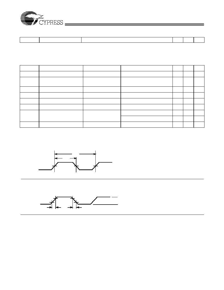
Switching Waveforms
Duty Cycle Timing
t
1B
t
1A
1.5V
1.5V
1.5V
All Outputs Rise/Fall Time
OUTPUT
t
2
t
3
3.3V
0V
0.4V
2.4V
2.4V
0.4V
t
2
t
4

CY2254A
Document #: 38-07203 Rev. *A
Page 5 of 8
Notes:
5.
All parameters specified with outputs fully loaded.
6.
Duty cycle is measured at 1.5V.
Switching Waveforms
(continued)
Clock Skew
CPUCLK/
PCICLK
1.5V
1.5V
t
5
t
6