 | –≠–ª–µ–∫—Ç—Ä–æ–Ω–Ω—ã–π –∫–æ–º–ø–æ–Ω–µ–Ω—Ç: CY2283 | –°–∫–∞—á–∞—Ç—å:  PDF PDF  ZIP ZIP |

PRELIMINARY
PentiumÆ/II, K6, 6x86 100-MHz Clock Synthesizer/Driver for
Desktop PCs with ALI or VIA Chipsets, AGP and 3 DIMMs
CY2283
Cypress Semiconductor Corporation
∑
3901 North First Street
∑
San Jose
∑
CA 95134
∑
408-943-2600
October 12, 1998
Features
∑ Mixed 2.5V and 3.3V operation
∑ Complete clock solution for PentiumÆ /II, Cyrix 6x86,
and AMD K6 processor-based motherboards
-- Four CPU clocks at 2.5V or 3.3V
-- Twelve 3.3V SDRAM clocks
[1]
-- Five synchronous PCI clocks, one free-running
-- One 3.3V 48 MHz USB clock
-- One 3.3V Ref. clock at 14.318 MHz
-- Two AGP clocks at 3.3V
∑ Support for ALI (-1 option) and VIA (-2 option)
∑ I
2
CTM Serial Configuration Interface
∑ Full EMI control with factory-EPROM programmable
output drive and slew rate
∑ Factory-EPROM programmable CPU clock frequencies
for custom configurations
∑ Power-down, CPU stop, and PCI stop pins
∑ Available in space-saving 48-pin SSOP package
Functional Description
The CY2283 is a clock Synthesizer/Driver for Pentium, Cyrix,
or AMD processor-based PCs using the ALI Aladdin V (-1 op-
tion) or VIA MVP3 (-2 option) chipset.
The CY2283 outputs four CPU clocks at 2.5V or 3.3V. There
are five PCI clocks, running at 30 or 33.3 MHz. One of the PCI
clocks is free-running. Additionally, the part outputs twelve
3.3V SDRAM clocks
[1]
, one 3.3V USB clock at 48 MHz, and
one 3.3V reference clock at 14.318 MHz. Finally, the part out-
puts two AGP clocks running at 66.66 MHz or 60 MHz.
The CY2283 has the flexibility to work as either a one-chip or
as part of a two-chip clocking solution. In 100-MHz board de-
signs based on the ALI Aladdin V chipset, it is recommended
that the CY2283 be used with an external SDRAM buffer so-
lution such as the CY2318NZ or CY2314NZ. In this configura-
tion the SDRAM outputs on the CY2283 must be either turned
off using I
2
C or left floating. The CY231xNZ family provides the
SDRAM outputs in place of the CY2283 and can be placed in
close proximity to the SDRAM modules.
The CY2283 possesses power-down, CPU stop, and PCI stop
pins for power management control. These inputs are multi-
plexed with SDRAM clock outputs, and are selected when the
MODE pin is driven LOW. Additionally, the signals are synchro-
nized on-chip, and ensure glitch-free transitions on the out-
puts. When the CPU_STOP input is asserted, the CPU clock
outputs are driven LOW. When the PCI_STOP input is assert-
ed, the PCI clock outputs (except the free-running PCI clock)
are driven LOW. When the PWR_DWN pin is asserted, the
reference oscillator and PLLs are shut down, and all outputs
are driven LOW.
The CY2283 outputs are designed for low EMI emissions.
Controlled rise and fall times, unique output driver circuits and
factory-EPROM programmable output drive and slew-rate en-
able optimal configurations for EMI control.
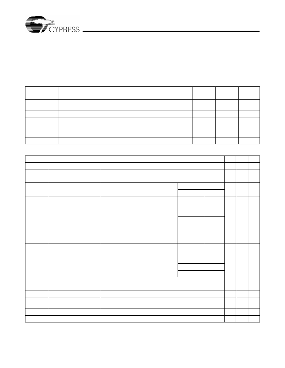
CY2283 Selector Guide
Notes:
1.
SDRAM clocks available up to 83.3MHz. In 100-MHz designs based on the
ALI V chipset, an external CY231xNZ buffer should be used.
2.
One free-running PCI clock
Clock Outputs
-1 (ALI V)
-2 (VIA MVP3)
CPU (66.6, 75, 83.3, 100MHz)
4
4
SDRAM
12
[1]
12
PCI (30, 33.3 MHz)
5
[2]
5
[2]
USB (48MHz)
1
1
AGP (66.6, 60MHz)
2
2
Ref. (14.318 MHz)
1
1
CPU-PCI delay
2.5
-
5.5 ns
2.5
-
5.5 ns
AGP clock
In phase
with PCI
In phase
with CPU
Pin Configuration (48 SSOP)
Logic Block Diagram
EPROM
XTALOUT
XTALIN
14.318
MHz
OSC.
SDRAM [0-4],[8-11]
SEL0
SDRAM7/PCI_STOP
CPU
PLL
MODE
SCLK
SDATA
REF0 (14.318 MHz)
CPUCLK [0-3]
V
DDCPU
SDRAM6/CPU_STOP
PCI [0-3]
PCICLK_F
STOP
STOP
LOGIC
LOGIC
SDRAM5/PWR_DWN
SEL1
USBCLK
SYS PLL
1
2
3
4
5
6
7
8
9
10
11
12
33
32
31
30
29
25
26
27
28
36
35
AV
DD
34
13
14
15
16
17
18
19
20
21
22
23
24
45
44
43
42
41
37
38
39
40
48
47
46
C
Y
2283-
1,-
2
REF0
V
SS
XTALIN
XTALOUT
PCICLK_F
V
DDQ3
PCICLK0
PCICLK1
V
SS
PCICLK2
PCICLK3
AGP0
AGP1
V
DDQ3
SDRAM11
SDRAM10
V
DDQ3
SDRAM9
SDRAM8
V
SS
SDATA
SCLK
V
DDQ3
USBCLK
SEL1
V
SS
CPUCLK0
CPUCLK1
V
DDCPU
CPUCLK2
CPUCLK3
V
SS
SDRAM0
SDRAM1
V
DDQ3
SDRAM2
SDRAM3
V
SS
SDRAM5/PWR_DWN
SDRAM6/CPU_STOP
SDRAM7/PCI_STOP
V
SS
SEL0
MODE
V
DDQ3
SDRAM4
V
SS
AGP
INTERFACE
CONTROL
LOGIC
SERIAL
Delay (-1 option)
/2
Delay (-2 option)
/1, /1.25, /1.5

CY2283
PRELIMINARY
2
Pin Summary
Name
Pins
Description
V
DDQ3
6, 14, 19, 30, 36, 48 3.3V Digital voltage supply
V
DDCPU
42
CPU Digital voltage supply, 2.5V or 3.3V
AV
DD
1
Analog voltage supply, 3.3V
V
SS
3, 9, 16, 22, 27, 33,
39, 45
Ground
XTALIN
[3]
4
Reference crystal input
XTALOUT
[3]
5
Reference crystal feedback
SDRAM7/ PCI_STOP
28
SDRAM clock output. Also, active LOW control input to stop PCI clocks, enabled
when MODE is LOW.
SDRAM6/CPU_STOP
29
SDRAM clock output. Also, active LOW control input to stop CPU clocks, enabled
when MODE is LOW.
SDRAM5/ PWR_DWN
31
SDRAM clock output. Also, active LOW control input to power down device,
enabled when MODE is LOW.
SDRAM[0:4],[8:11]
38, 37, 35, 34, 32,
21, 20, 18, 17
SDRAM clock outputs
SEL0
26
CPU frequency select input, bit 0 (see table below)
SEL1
46
CPU frequency select input, bit 0 (see table below)
CPUCLK[0:3]
44, 43, 41, 40
CPU clock outputs
PCICLK[0:3]
8, 10, 11, 12
PCI clock outputs, at one-half the CPU frequency.
PCICLK_F
7
Free-running PCI clock output
AGP[0:1]
13, 15
AGP clock outputs
REF0
2
3.3V Reference clock output
USBCLK
47
USB Clock output
SDATA
23
Serial data input for serial configuration port
SCLK
24
Serial clock input for serial configuration port
MODE
25
Mode Select pin for enabling power management features
Note:
3.
For best accuracy, use a parallel-resonant crystal, C
LOAD
= 18 pF.
Function Table
SEL1
SEL0
CPU/PCI
Ratio
CPUCLK[0:3]
SDRAM[0:11]
PCICLK[0:3]
PCICLK_F
AGP[0:1]
REF0
USBCLK
0
0
2.5
83.33 MHz
33.33 MHz
66.66 MHz
14.318 MHz
48 MHz
0
1
2
66.67 MHz
33.33 MHz
66.66 MHz
14.318 MHz
48 MHz
1
0
3.0
100.0 MHz
33.33 MHz
66.66 MHz
14.318 MHz
48 MHz
1
1
2.5
75.0 MHz
30.0 MHz
60.0 MHz
14.318 MHz
48 MHz

CY2283
PRELIMINARY
3
CPU and PCI Clock Driver Strengths
∑ Matched impedances on both rising and falling edges on
the output drivers
∑ Output impedance: 25
(typical) measured at 1.5V
Serial Configuration Map
∑ The Serial bits will be read by the clock driver in the following
order:
Byte 0 - Bits 7, 6, 5, 4, 3, 2, 1, 0
Byte 1 - Bits 7, 6, 5, 4, 3, 2, 1, 0
.
.
Byte N - Bits 7, 6, 5, 4, 3, 2, 1, 0
∑ Reserved and unused bits should be programmed to "0".
∑ I
2
C Address for the CY2283 is:
Actual Clock Frequency Values
Clock Output
Target
Frequency
(MHz)
Actual
Frequency
(MHz)
PPM
CPUCLK
66.67
66.51
≠2346
CPUCLK
75.0
75.0
0
CPUCLK
83.33
83.14
-2346
CPUCLK
100.0
99.77
-2346
USBCLK
48.0
48.01
167
Power Management Logic
[4]
- Active when MODE pin is held `LOW'
CPU_STOP
PCI_STOP
PWR_DWN
CPUCLK
PCICLK
PCICLK_F
Other
Clocks
Osc.
PLLs
X
X
0
Low
Low
Stopped
Stopped
Off
Off
0
0
1
Low
Low
Running
Running
Running
Running
0
1
1
Low
33/30 MHz
Running
Running
Running
Running
1
0
1
66/75/83/100MHz
Low
Running
Running
Running
Running
1
1
1
66/75/83/100MHz
30/33.3 MHz
Running
Running
Running
Running
A6
A5
A4
A3
A2
A1
A0
R/W
1
1
0
1
0
0
1
----
Byte 0: Functional and Frequency Select Clock
Register (1 = Enable, 0 = Disable)
Bit
Pin #
Description
Bit 7
--
(Reserved) drive to `0'
Bit 6
--
(Reserved) drive to `0'
Bit 5
--
(Reserved) drive to `0'
Bit 4
--
(Reserved) drive to `0'
Bit 3
--
(Reserved) drive to `0'
Bit 2
--
(Reserved) drive to `0'
Bit 1
Bit 0
--
Bit 1
1
1
0
0
Bit 0
1 - Three-State
0 - N/A
1 - Testmode
0 - Normal Operation
Select Functions
Functional Description
Outputs
CPU
PCI, PCI_F
SDRAM
Ref
IOAPIC
USBCLK
AGP
Three-State
Hi-Z
Hi-Z
Hi-Z
Hi-Z
Hi-Z
Hi-Z
Hi-Z
Test Mode
[6]
TCLK/2
[5]
TCLK/4
TCLK/2
TCLK
TCLK
TCLK/2
TCLK/2
Notes:
4.
AGP clocks are free-running and stop only when the PWR_DWN pin is asserted. The frequency of the AGP clocks is as shown in the Function Table.
5.
TCLK supplied on the XTALIN pin in Test Mode.
6.
Valid only for SEL1=0.

CY2283
PRELIMINARY
4
Byte 1: CPU Active/Inactive Register
(1 = Active, 0 = Inactive), Default = Active
Bit
Pin #
Description
Bit 7
47
USBCLK
Bit 6
N/A
(Reserved) drive to `0'
Bit 5
N/A
(Reserved) drive to `0'
Bit 4
N/A
Not used - drive to `0'
Bit 3
40
CPUCLK3 (Active/Inactive)
Bit 2
41
CPUCLK2 (Active/Inactive)
Bit 1
43
CPUCLK1 (Active/Inactive)
Bit 0
44
CPUCLK0 (Active/Inactive)
Byte 3: SDRAM Active/Inactive Register
(1 = Active, 0 = Inactive), Default = Active
Bit
Pin #
Description
Bit 7
28
SDRAM7 (Active/Inactive)
Bit 6
29
SDRAM6 (Active/Inactive)
Bit 5
31
SDRAM5 (Active/Inactive)
Bit 4
32
SDRAM4 (Active/Inactive)
Bit 3
34
SDRAM3 (Active/Inactive)
Bit 2
35
SDRAM2 (Active/Inactive)
Bit 1
37
SDRAM1 (Active/Inactive)
Bit 0
38
SDRAM0 (Active/Inactive)
Byte 5: Peripheral Active/Inactive Register
(1 = Active, 0 = Inactive), Default = Active
Bit
Pin #
Description
Bit 7
N/A
(Reserved) drive to `0'
Bit 6
N/A
(Reserved) drive to `0'
Bit 5
N/A
(Reserved) drive to `0'
Bit 4
N/A
(Reserved), drive to `0'
Bit 3
N/A
(Reserved) drive to `0'
Bit 2
N/A
(Reserved) drive to `0'
Bit 1
N/A
(Reserved) drive to `0'
Bit 0
2
REF0 (Active/Inactive)
Byte 2: PCI Active/Inactive Register
(1 = Active, 0 = Inactive), Default = Active
Bit
Pin #
Description
Bit 7
--
(Reserved) drive to `0'
Bit 6
7
PCICLK_F (Active/Inactive)
Bit 5
15
AGP1 (Active/Inactive)
Bit 4
14
AGP0 (Active/Inactive)
Bit 3
12
PCICLK3 (Active/Inactive)
Bit 2
11
PCICLK2 (Active/Inactive)
Bit 1
10
PCICLK1 (Active/Inactive)
Bit 0
8
PCICLK0 (Active/Inactive)
Byte 4: SDRAM Active/Inactive Register
(1 = Active, 0 = Inactive), Default = Active
Bit
Pin #
Description
Bit 7
N/A
Not used - drive to `0'
Bit 6
N/A
Not used - drive to `0'
Bit 5
N/A
Not used - drive to `0'
Bit 4
N/A
Not used - drive to `0'
Bit 3
17
SDRAM11
Bit 2
18
SDRAM10
Bit 1
20
SDRAM9
Bit 0
21
SDRAM8
Byte 6: Reserved, for future use
CY2283
PRELIMINARY
5
Maximum Ratings
(Above which the useful life may be impaired. For user guide-
lines, not tested.)
Supply Voltage ..................................................≠0.5 to +7.0V
Input Voltage .............................................. ≠0.5V to V
DD
+0.5
Storage Temperature (Non-Condensing) ... ≠65
∞
C to +150
∞
C
Max. Soldering Temperature (10 sec) ...................... +260
∞
C
Junction Temperature ............................................... +150
∞
C
Package Power Dissipation .............................................. 1W
Static Discharge Voltage ........................................... >2000V
(per MIL-STD-883, Method 3015, like V
DD
pins tied together)
Operating Conditions
[7]
Parameter
Description
Min.
Max.
Unit
AV
DD
, V
DDQ3
Analog and Digital Supply Voltage
3.135
3.465
V
V
DDCPU
CPU Supply Voltage
2.375
3.135
2.9
3.465
V
T
A
Operating Temperature, Ambient
0
70
∞
C
C
L
Max. Capacitive Load on
CPUCLK, USBCLK, IOAPIC
PCICLK, AGP, SDRAM
REF0
10
20
20
20
30
45
pF
f
(REF)
Reference Frequency, Oscillator Nominal Value
14.318
14.318
MHz
Electrical Characteristics
Over the Operating Range
Parameter
Description
Test Conditions
Min. Max. Unit
V
IH
High-level Input Voltage
Except Crystal Inputs
2.0
V
V
IL
Low-level Input Voltage
Except Crystal Inputs
0.8
V
V
ILiic
Low-level Input Voltage
I
2
C inputs only
0.7
V
V
OH
High-level Output Voltage
V
DDCPU
= V
DDQ2
= 2.375V
I
OH
= 16 mA CPUCLK
2.0
V
I
OH
= 18 mA IOAPIC
V
OL
Low-level Output Voltage
V
DDCPU
= V
DDQ2
= 2.375V
I
OL
= 27 mA
CPUCLK
0.4
V
I
OL
= 29 mA
IOAPIC
V
OH
High-level Output Voltage
V
DDQ3
, AV
DD
, V
DDCPU
= 3.135V
I
OH
= 16 mA CPUCLK
2.4
V
I
OH
= 36 mA SDRAM
I
OH
= 32 mA PCICLK
I
OH
= 26 mA USBCLK
I
OH
= 36 mA REF0
V
OL
Low-level Output Voltage
V
DDQ3
, AV
DD
, V
DDCPU
= 3.135V
I
OL
= 27 mA
CPUCLK
0.4V
V
I
OL
= 29 mA
SDRAM
I
OL
= 26 mA
PCICLK
I
OL
= 21 mA
USBCLK
I
OL
= 29 mA
REF0
I
IH
Input High Current
V
IH
= V
DD
≠10
+10
µ
A
I
IL
Input Low Current
V
IL
= 0V
10
µ
A
I
OZ
Output Leakage Current
Three-state
≠10
+10
µ
A
I
DD
Power Supply Current
[8]
V
DD
= 3.465V, V
IN
= 0 or V
DD
, Loaded Outputs,
CPU clocks = 66.67 MHz
300
mA
I
DD
Power Supply Current
[8]
V
DD
= 3.465V, V
IN
= 0 or V
DD
, Unloaded Outputs
120
mA
I
DDS
Power-down Current
Current draw in power-down state
500
µ
A
Notes:
7.
Electrical parameters are guaranteed with these operating conditions.
8.
Power supply current will vary with number of outputs that are running.