
100-MHz Spread Spectrum Clock Synthesizer/Driver with
USB, Hublink, and SDRAM Support
CY2287
Cypress Semiconductor Corporation
∑
3901 North First Street
∑
San Jose
∑
CA 95134
∑
408-943-2600
June 23, 1999
Features
Benefits
∑ Mixed 2.5V and 3.3V Operation
Usable with Pentium
II, K6, and 6x86 Processors
∑ Multiple output clocks at different frequencies
-- Three CPU clocks at 2.5V, up to 100 MHz
-- Nine 3.3V SDRAM clocks at 100 MHz
-- Eight synchronous PCI clocks at 33 MHz
-- Two synchronous APIC clocks at 16.67 MHz or 33
MHz
-- Two 3V66 clocks at 66 MHz
-- Two USB clocks at 48 MHz
-- One reference clock at 14.318 MHz
Single-chip main motherboard clock generator
-- High-Speed Processor Support
-- Supports Two 4-Clock SDRAM DIMMs
-- Support for Six PCI Slots
-- Synchronous to the CPU Clock
-- Hublink Support
-- Universal Serial Bus Support
-- Also used as an input strap to determine APIC frequency
∑ Spread Spectrum clocking
-- 31 kHz modulation frequency
-- EPROM programmable percentage of spreading
-- Default is ≠0.6%, which is recommended by IntelÆ
-- Additional options of ≠0.25% and ≠0.4% available
Enables reduction of EMI
∑ Power-down features
Supports mobile systems
∑ I
2
CTM Interface
Dynamic output control
∑ Low skew and low jitter outputs
Meets tight system timing requirements at high frequency
∑ Test Mode
Enables ATE and "bed of nails" testing
∑ 56-pin SSOP package
Widely available, standard package enables lower cost
Intel and Pentium are registered trademarks of Intel Corporation.
I
2
C is a trademark of Philips Corporation.
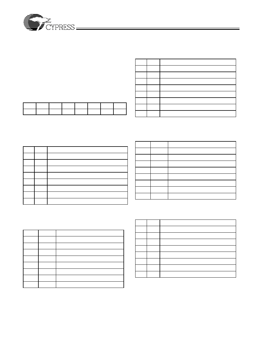
SERIAL INTERFACE
CONTROL LOGIC
Logic Block Diagram
EPROM
XTALOUT
XTALIN
APIC [0≠1] (16.67/33MHz)
14.318
MHz
OSC.
SDRAM [0-8] (100 MHz)
SEL1
CPU
PLL
REF0/SEL33 (14.318 MHz)
CPU [0≠2] (66/100 MHz)
PCI [0≠7] (33MHz)
SYS
PLL
USB [0≠1] (48MHz)
EPROM
Configurable
Logic
PWR_DWN
3V66 [0≠1] (66MHz)
SSOP
Top View
1
2
3
4
5
6
7
8
9
10
11
12
33
32
31
30
29
36
35
REF0/SEL33
34
13
14
15
16
17
18
19
20
21
22
23
24
45
44
43
42
41
37
38
39
40
48
47
46
V
DDREF
XTAL_IN
XTAL_OUT
25
26
27
28
49
52
51
50
53
56
55
54
V
DDPCI
V
SSPCI
AV
SS
SCLK
SDRAM8
SDRAM4
V
SSSDRAM
V
DDAPIC
3V66_0
PCI3
PCI7
USB1
SDRAM6
SDRAM2
CPU1
V
SSAPIC
V
SSREF
V
SS3V66
3V66_1
V
DD3V66
PCI0
PCI1
PCI2
V
SSPCI
PCI4
PCI5
PCI6
V
DDPCI
AV
DD
V
SSUSB
USB0
V
DDSDRAM
PWRDWN
V
SSSDRAM
SDRAM7
V
DDSDRAM
SDRAM5
V
SSSDRAM
SDRAM3
V
DDSDRAM
SDRAM1
SDRAM0
V
SSCPU
CPU2
V
DDCPU
CPU0
APIC1
APIC0
V
DDUSB
SEL0
SDATA
SEL1
CY2287
SCLK
SDATA
SEL0

CY2287
2
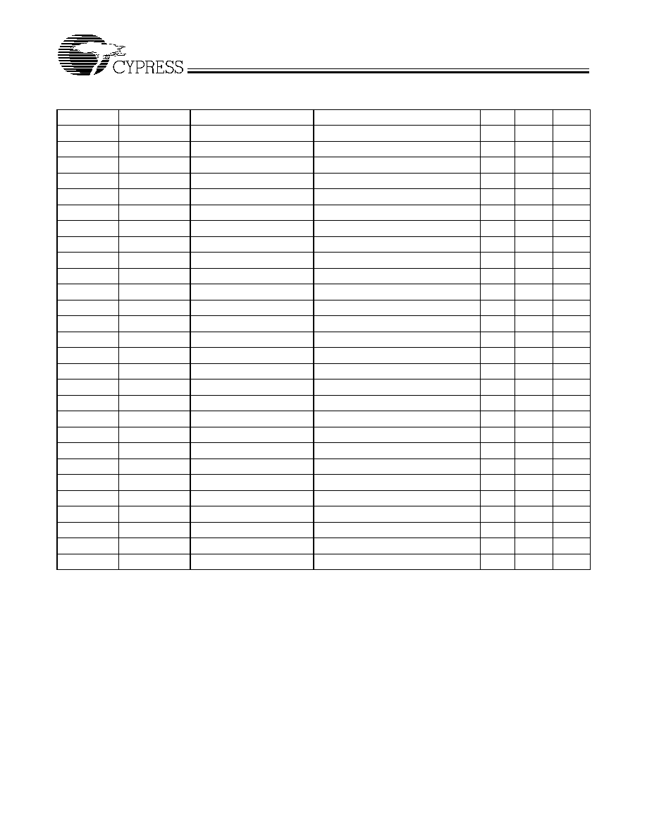
Pin Summary
Name
Pins
Description
REF/SEL33
1
3.3V 14.31818-MHz clock output and power-on external select strap op-
tion for APIC clock frequency.
Strap LOW: APIC = PCI/2
Strap HIGH: APIC = 33.3 MHz
XTAL_IN
[1]
3
14.31818-MHz crystal input
XTAL_OUT
[1]
4
14.31818-MHz crystal output
PCI [0≠7]
11, 12, 13, 15, 16, 18, 19, 20
3.3V PCI clock outputs
3V66 [0≠1]
7, 8
3.3V Fixed 66.67-MHz clock outputs
USB [0≠1]
25, 26
3.3V Fixed 48-MHz clock outputs
SEL [0≠1]
28, 29
3.3V LVTTL compatible inputs for logic selection
PWRDWN
32
3.3V LVTTL compatible input. Device enters powerdown mode when held
LOW
CPU [0≠2]
49, 50, 52
2.5V 66.67-MHz or 100-MHz (selectable) host bus clock output
SDRAM [0≠8]
35, 36, 37, 39, 40, 42, 43, 45, 46 3.3V SDRAM clock outputs running 100 MHz
APIC [0≠1]
54, 55
2.5V APIC clock outputs running synchronous with PCI clock frequency.
Selectable 16.67 MHz or 33.3 MHz
SDATA
30
I
2
C compatible SDATA input
SCLK
31
I
2
C compatible SCLK input
V
DDREF
2
3.3V Power supply for REF output
V
SSREF
5
REF ground
V
SS3V66
6
3V66 Ground
V
DD3V66
9
3.3V Power supply for 3V66 outputs
V
DDPCI
10, 21
3.3V Power supply for PCI outputs
V
SSPCI
14, 17
PCI ground
AV
DD
22
3.3V Analog power supply
AV
SS
23
Analog ground
V
SSUSB
24
USB ground
V
DDUSB
27
3.3V Power supply for USB outputs
V
DDSDRAM
33, 38, 44
3.3V Power supply for SDRAM outputs
V
SSSDRAM
35, 41, 47
SDRAM ground
V
SSCPU
48
CPU ground
V
DDCPU
51
2.5V Power supply for CPU outputs
V
DDAPIC
53
2.5V Power supply for APIC outputs
V
SSAPIC
56
APIC ground
Note:
1.
For best accuracy, use a parallel-resonant crystal, C
LOAD
= 18 pF. For crystals with different C
LOAD
, please refer to the application note, "Crystal Oscillator
Topics."

CY2287
3
Function Table
SEL2
[2]
SEL1
SEL0
CPU
(MHz)
SDRAM
(MHz)
3V66
(MHz)
PCI
(MHz)
USB
(MHz)
REF
(MHz)
APIC
[4]
(MHz)
APIC
[5]
(MHz)
0
0
0
Hi-Z
Hi-Z
Hi-Z
Hi-Z
Hi-Z
Hi-Z
Hi-Z
Hi-Z
0
0
1
TCLK
[3]
/2
TCLK/2
TCLK/3
TCLK/8
TCLK/2
TCLK
TCLK/16
TCLK/8
0
1
0
66.67
100
66.67
33.33
48
14.318
16.67
33.33
0
1
1
100
100
66.67
33.33
48
14.318
16.67
33.33
1
0
0
66.67
100
66.67
33.33
48
14.318
16.67
33.33
1
0
1
100
100
66.67
33.33
48
14.318
16.67
33.33
1
1
0
66.67
100
66.67
33.33
48
14.318
16.67
33.33
1
1
1
100
100
66.67
33.33
48
14.318
16.67
33.33
Spread Spectrum
[2]
SEL2
[2]
SEL1
SEL0
Spread Spectrum Margin
X
0
0
0
N/A
X
0
0
1
N/A
0
X
X
X
N/A
1
0
1
0
≠0.6%
1
0
1
1
≠0.6%
1
1
0
0
≠0.25%
1
1
0
1
≠0.25%
1
1
1
0
≠0.4%
1
1
1
1
≠0.4%
Actual Clock Frequency Values
Clock Output
Target
Frequency (MHz)
Actual
Frequency (MHz)
PPM
CPUCLK
66.67
66.288
≠5230
CPUCLK
100.0
99.432
≠5680
USBCLK
48.0
48.008
+167
Notes:
2.
Not a dedicated input pin. This selection must be addressed via I
2
C interface.
3.
TCLK supplied on the XTALIN pin in Test Mode.
4.
SEL33 = LOW (power-on latch input).
5.
SEL33 = HIGH (power-on latch input).
CY2287
4
Serial Configuration Map
∑ The Serial bits will be read by the clock driver in the following
order:
Byte 0 - Bits 7, 6, 5, 4, 3, 2, 1, 0
Byte 1 - Bits 7, 6, 5, 4, 3, 2, 1, 0
.
.
Byte N - Bits 7, 6, 5, 4, 3, 2, 1, 0
∑ Reserved and unused bits must be programmed to "0".
∑ I
2
C Address for the CY2287 is:
A6
A5
A4
A3
A2
A1
A0
R/W
1
1
0
1
0
0
1
0
Byte 0: Spread Spectrum, USB, SDRAM8
Control Register
(1 = Enable, 0 = Disable)
Default = Enable (for Bit [0:2])
Default = Disable (for Bit [3:7])
Bit
Pin #
Description
Bit 7 --
Reserved
Bit 6 --
Reserved
Bit 5 --
Reserved
Bit4
--
SEL2
Bit3
--
Spread Spectrum (Default = Disable)
Bit2
26
USB1
Bit1
25
USB0
Bit0
49
CPU2
Byte 1: SDRAM Control Register
(1 = Enable, 0 = Disable)
Default = Enable
Bit
Pin #
Description
Bit 7
36
SDRAM7
Bit 6
37
SDRAM6
Bit 5
39
SDRAM5
Bit 4
40
SDRAM4
Bit 3
42
SDRAM3
Bit 2
43
SDRAM2
Bit 1
45
SDRAM1
Bit 0
46
SDRAM0
Byte 2: PCI Control Register
(1 = Enable, 0 = Disable)
Default = Enable (for Bit [1:7])
Default = Disable (for Bit 0)
Bit
Pin #
Description
Bit 7
20
PCI7
Bit 6
19
PCI6
Bit 5
18
PCI5
Bit 4
16
PCI4
Bit 3
15
PCI3
Bit 2
13
PCI2
Bit 1
12
PCI1
Bit 0
11
Reserved
Byte 3: Peripheral Control Register
(0 = Enable, 1 = Disable)
Default = Enable
Bit
Pin #
Description
Bit 7
8
3V66_1
Bit 6
7
3V66_0
Bit 5
11
PCI0
Bit 4
34
SDRAM8
Bit 3
54
APIC1
Bit 2
55
APIC0
Bit 1
50
CPU1
Bit 0
52
CPU0
Byte 4: Reserved Register
(0 = Enable, 1 = Disable)
Default = Disable
Bit
Pin #
Description
Bit 7
--
Reserved
Bit 6
--
Reserved
Bit 5
--
Reserved
Bit 4
--
Reserved
Bit 3
--
Reserved
Bit 2
--
Reserved
Bit 1
--
Reserved
Bit 0
--
Reserved

CY2287
5
Maximum Ratings
(Above which the useful life may be impaired. For user guide-
lines, not tested.)
Supply Voltage ..................................................≠0.5 to +7.0V
Input Voltage .............................................. ≠0.5V to V
DD
+0.5
Storage Temperature (Non-Condensing) ... ≠65∞C to +150∞C
Max. Soldering Temperature (10 sec) ...................... +260∞C
Junction Temperature ............................................... +150∞C
Package Power Dissipation .............................................. 1W
Static Discharge Voltage
(per MIL-STD-883, Method 3015) ............................. >2000V
Operating Conditions
Over Which Electrical Parameters are Guaranteed
Parameter
Description
Min.
Max.
Unit
V
DD3.3V
3.3V Supply Voltages
3.135
3.465
V
V
DD2.5V
2.5V Supply Voltages
2.375
2.625
V
T
A
Operating Temperature, Ambient
0
70
∞C
C
L
Max. Capacitive Load on
CPU, USB, REF, APIC
SDRAM, PCI, 3V66
20
30
pF
f
(REF)
Reference Frequency, Oscillator Nominal Value
14.318
14.318
MHz
Electrical Characteristics
Over the Operating Range
Parameter
Description
Test Conditions
Min.
Typ
Max. Unit
V
IH
High-level Input Voltage
All inputs except SCLK/SDATA and crystal inputs
[6]
2.0
V
SCLK/SDATA
0.7
V
DD
V
IL
Low-level Input Voltage
All inputs except SCLK/SDATA and crystal inputs
[6]
0.8
V
SCLK/SDATA
0.3
V
DD
I
IH
Input High Current
0 < V
IN
< V
DD
≠10
+10
µ
A
I
IL
Input Low Current
0 < V
IN
< V
DD
≠10
+10
µ
A
I
OH
High-level Output Current
CPU
V
OH
= 2.0V
≠16
-60
mA
USB, REF
V
OH
= 2.4V
≠15
≠51
SDRAM
V
OH
= 2.4V
≠30
≠100
PCI, 3V66
V
OH
= 2.4V
≠30
≠100
APIC
V
OH
= 2.0V
≠16
-60
I
OL
Low-level Output Current
CPU
V
OL
= 0.4V
19
49
mA
USB, REF
V
OL
= 0.4V
10
24
SDRAM
V
OL
= 0.4V
20
49
PCI, 3V66
V
OL
= 0.4V
20
49
APIC
V
OL
= 0.4V
19
49
I
OZ
Output Leakage Current
Three-state
10
µ
A
I
DD2
2.5V Power Supply Current
AV
DD
/V
DD33
= 3.465V, V
DD25
= 2.625V, F
CPU
= 100 MHz
100
mA
I
DD3
3.3V Power Supply Current
AV
DD
/V
DD33
= 3.465V, V
DD25
= 2.625V, F
CPU
= 100 MHz
280
mA
I
DDPD2
2.5V Shutdown Current
AV
DD
/V
DD33
= 3.465V, V
DD25
= 2.625V
[7]
<1
500
µ
A
I
DDPD3
3.3V Shutdown Current
AV
DD
/V
DDQ3
= 3.465V, V
DD25
= 2.625V
[7]
<9
500
µ
A
Notes:
6.
Crystal inputs have CMOS thresholds, nominally V
DD
/2.
7.
Tested @ 500
µ
A. Actual performance is much better. Call Cypress if tighter spec is required.
CY2287
6
CY2287 Switching Characteristics
[8]
Over the Operating Range
Parameter
Output
Description
Test Conditions
Min.
Max.
Unit
t
1
All
Output Duty Cycle
[9]
t
1A
/(t
1A
+ t
1B
)
45
55
%
t
2
CPU, APIC
Rising Edge Rate
Between 0.4V and 2.0V
1.0
4.0
V/ns
t
2
USB, REF
Rising Edge Rate
Between 0.4V and 2.4V
0.5
2.0
V/ns
t
2
PCI, 3V66
Rising Edge Rate
Between 0.4V and 2.4V
1.0
4.0
V/ns
t
2
SDRAM
Rising Edge Rate
Between 0.4V and 2.4V
1.0
4.0
V/ns
t
3
CPU, APIC
Falling Edge Rate
Between 2.0V and 0.4V
1.0
4.0
V/ns
t
3
USB, REF
Falling Edge Rate
Between 2.4V and 0.4V
0.5
2.0
V/ns
t
3
PCI, 3V66
Falling Edge Rate
Between 2.4V and 0.4V
1.0
4.0
V/ns
t
3
SDRAM
Falling Edge Rate
Between 2.4V and 0.4V
1.0
4.0
V/ns
t
4
CPU
CPU-CPU Skew
Measured at 1.25V
175
ps
t
4
SDRAM
SDRAM-SDRAM Skew
Measured at 1.5V
250
ps
t
4
APIC
APIC-APIC Skew
Measured at 1.25V
250
ps
t
4
PCI
PCI-PCI Skew
Measured at 1.5V
500
ps
t
4
3V66
3V66-3V66 Skew
Measured at 1.5V
175
ps
t
4
3V66, PCI
3V66-PCI Clock Skew
3V66 leads
[10]
1.5
4.0
ns
t
4
APIC, PCI
APIC-PCI Clock Skew
Coincident every edge
[10, 11]
500
ps
t
5
SDRAM, 3V66
SDRAM-3V66 Clock Skew
Coincident every other 3V66 edge
[10]
500
ps
t
6_66
CPU, 3V66
CPU-3V66 Clock Skew
CPU leads
[10]
7.0
8.0
ns
t
6_100
CPU, 3V66
CPU-3V66 Clock Skew
Coincident every other 3V66 edge
[10]
500
ps
t
7_66
CPU, SDRAM
CPU-SDRAM Clock Skew
SDRAM leads
[10, 12]
2.0
3.0
ns
t
7_100
CPU, SDRAM
CPU-SDRAM Clock Skew
CPU leads, measured every edge
[10]
4.5
5.5
ns
t
8
CPU
Cycle-Cycle Clock Jitter
Measured at 1.25V, t
8A
≠ t
8B
250
ps
t
8
SDRAM
Cycle-Cycle Clock Jitter
Measured at 1.5V, t
8A
≠ t
8B
250
ps
t
8
APIC
Cycle-Cycle Clock Jitter
Measured at 1.25V, t
8A
≠ t
8B
500
ps
t
8
USB
Cycle-Cycle Clock Jitter
Measured at 1.5V, t
8A
≠ t
8B
500
ps
t
8
3V66
Cycle-Cycle Clock Jitter
Measured at 1.5V, t
8A
≠ t
8B
500
ps
t
8
REF
Cycle-Cycle Clock Jitter
Measured at 1.5V, t
8A
≠ t
8B
1000
ps
t
STABLE
All Outputs
Settle Time
All clock stabilization from power-up
3
ms
Notes:
8.
All parameters specified with loaded outputs as follows: CPU, APIC, REF, USB = 12.5 pF: SDRAM, 3V66, PCI=20 pF.
9.
Duty cycle is measured at 1.5V when V
DD
= 3.3V. When V
DD
= 2.5V, duty cycle is measured at 1.25V.
10. Measured at 1.25V for 2.5V clocks and 1.5V for 3.3V clocks.
11. Coincident every other APIC edge if APIC running at 16 MHz.
12. Measured every third CPU edge.

CY2287
7
Switching Waveforms
Notes:
13. Once the PWR_DWN signal is sampled LOW for two consecutive rising edges of CPU clock, clocks of interest will be held LOW on the next HIGH-to-LOW
transition.
14. Waveforms are not to scale.
15. Shaded section on the VCO and Crystal waveforms indicates that the VCO and crystal oscillator are active, and there is a valid clock.
Duty Cycle Timing
t
1A
t
1B
All Outputs Rise/Fall Time
OUTPUT
t
2
V
DD
0V
t
3
CLK-CLK Output Skew
t
4
CLKA
CLKB
Cycle-Cycle Clock Jitter
CLK
t
8A
t
8B
PWR_DOWN
CPUCLK
Peripheral
PWR_DWN
VCO
Crystal
Clocks
[13, 14, 15]

CY2287
8
Switching Waveforms
(continued)
CPU 66 MHz
SDRAM 100 MHz
3V66 66 MHz
0 ns
10 ns
20 ns
30 ns
40 ns
SDRAM to 3V66 Skew, SDRAM leads 3V66 by 0.0 ns (500-ps window)
t
5
CLK-CLK Output Skew (CPU @ 66 MHz)
CPU 66 MHz
3V66 66 MHz
0 ns
10 ns
20 ns
30 ns
40 ns
CPU to 3V66 Skew, CPU leads 3V66 by 7.5ns (500-ps window)
CLK-CLK Output Skew (CPU @ 66 MHz)
t
6_66
SDRAM 100 MHz
CPU 66 MHz
SDRAM 100 MHz
0 ns
10 ns
20 ns
30 ns
40 ns
CPU to SDRAM Skew, SDRAM leads CPU by 2.5 ns (500-ps window)
3V66 66 MHz
CLK-CLK Output Skew (CPU @ 66 MHz)
t
7_66

CY2287
9
Switching Waveforms
(continued)
CPU 100 MHz
SDRAM 100 MHz
3V66 66 MHz
0 ns
10 ns
20 ns
30 ns
40 ns
SDRAM to 3V66 Skew, SDRAM leads 3V66 by 0.0 ns (500-ps window)
t
5
CLK-CLK Output Skew (CPU @ 100 MHz)
CPU 100 MHz
SDRAM 100 MHz
3V66 66 MHz
0 ns
10 ns
20 ns
30 ns
40 ns
CPU to 3V66 Skew, CPU leads 3V66 by 0.0 ns (500-ps window)
CLK-CLK Output Skew (CPU @ 100 MHz)
t
6_100
CPU 100 MHz
SDRAM 100 MHz
0 ns
10 ns
20 ns
30 ns
40 ns
CPU to SRAM Skew, CPU leads SDRAM by 5.0 ns (500-ps window)
3V66 66 MHz
t
7_100
CLK-CLK Output Skew (CPU @ 100 MHz)

CY2287
10
Switching Waveforms
(continued)
Group A
Group B
1.5V
1.5V
Window Measurement Clarification
Example of SDRAM to 3V66 Skew Measurement (CPU @ 66 or 100 MHz)
SDRAM leads 3V66 by 0.0 ns (500-ps window)
500-ps window
Latest of Group B
Earliest of Group A
CPU Group
3V66 Group
1.5V
1.25V
Window Measurement Clarification
Example of CPU to 3V66 Skew Measurement (CPU @ 66 MHz)
CPU leads 3V66 by 7.5 ns (500-ps window)
8.0-ns window (max)
Latest of 3V66 Group
Earliest of CPU Group
Latest of CPU Group
Earliest of 3V66 Group
7.0-ns window (min)

CY2287
11
Switching Waveforms
(continued)
Frequency (MHz)
Am
p
lit
u
d
e
(
d
B)
Spread Spectrum Enabled
Spread Spectrum Disabled
SPREAD SPECTRUM CLOCKING
Description
Max.
Unit
Output
Min.
Down Spread Margin at the Fundamental Frequency
CPU, PCI, SDRAM, APIC, 3V66
≠0.6
%
Modulation Frequency
30.0
33.0
kHz
CPU, PCI, SDRAM, APIC, 3V66
≠0.25
Selectable Downspread Margins
≠0.25%
≠0.4%
≠0.6%

CY2287
12
Application Information
Clock traces must be terminated with either series or parallel termination, as they are normally done.
Application Circuit
Summary
∑ A parallel-resonant crystal should be used as the reference to the clock generator. The operating frequency and C
LOAD
of
this crystal should be as specified in the data sheet. Optional trimming capacitors may be needed if a crystal with a different
C
LOAD
is used. Footprints must be laid out for flexibility.
∑ Surface mount, low-ESR, ceramic capacitors should be used for filtering. Typically, these capacitors have a value of 2.2 nF.
In some cases, smaller value capacitors may be required.
∑ The value of the series terminating resistor satisfies the following equation, where R
trace
is the loaded characteristic impedance
of the trace, R
out
is the output impedance of the clock generator (CPU/APIC = 29 Ohm, USB/REF = 40 Ohm, SDRAM (3.3V)=
16 Ohm, PCI/3V66 = 30 Ohm - all nominal driver output impedances), and R
series
is the series terminating resistor.
R
series
> R
trace
≠ R
out
∑ Footprints must be laid out for optional EMI-reducing capacitors, which should be placed as close to the terminating resistor
as is physically possible. Typical values of these capacitors range from 4.7 pF to 22 pF.
∑ A Ferrite Bead may be used to isolate the Board V
DD
from the clock generator V
DD
island. Ensure that the Ferrite Bead offers
greater than 50
impedance at the clock frequency, under loaded DC conditions. Please refer to the application note "Layout
and Termination Techniques for Cypress Clock Generators" for more details.
∑ If a Ferrite Bead is used, a 10
µ
F≠ 22
µ
F tantalum bypass capacitor should be placed close to the Ferrite Bead. This capacitor
prevents power supply droop during current surges.
XTALIN
XTALOUT
PWR_DWN
SEL0
SEL1
PWR_DWN
Rs
Ct
VDD3.3V
VDD2.5V
VSS
CPU
PCI
HUBLINK
SDRAM
APIC
REF
USB
CPU
PCI
3V66
SDRAM
APIC
REF
USB
Cx
Cd
Cd
CY2287-1 56 Pin SSOP
Cd = Decoupling Capacitors (
NOTE: May use 0.1
µ
F, but value will vary with frequency of operation and output current
)
Ct = Optional EMI-Reducing Capacitors
Cx = Optional Load Matching Capacitors
Rs = Termination Resistor
3.3V VDD
2.5V VDD
SEL0
SEL1

CY2287
cy2287: May 26, 1998
Revision: June 23, 1999
© Cypress Semiconductor Corporation, 1999. The information contained herein is subject to change without notice. Cypress Semiconductor Corporation assumes no responsibility for the use
of any circuitry other than circuitry embodied in a Cypress Semiconductor product. Nor does it convey or imply any license under patent or other rights. Cypress Semiconductor does not authorize
its products for use as critical components in life-support systems where a malfunction or failure may reasonably be expected to result in significant injury to the user. The inclusion of Cypress
Semiconductor products in life-support systems application implies that the manufacturer assumes all risk of such use and in doing so indemnifies Cypress Semiconductor against all charges.
Document #: 38≠00711≠A
Test Circuit
Note: All capacitors must be placed as close to the pins as is physically possible.
5, 6, 14, 17, 23, 24, 34, 41, 47, 48, 56
2, 9, 10, 21, 22, 27, 32, 38, 44
V
DD3.3V
C
LOAD
OUTPUTS
V
DD2.5V
CY2287
51, 53
Note: Each supply pin must have an individual decoupling capacitor.
Ordering Information
Ordering Code
Package
Name
Package Type
Operating
Range
CY2287PVC≠1
O56
56-Pin SSOP
Commercial
Package Diagram
56-Lead Shrunk Small Outline Package O56
51-85062-B