PRELIMINARY
2.5V or 3.3V,10- 220 MHz, Low Jitter, 5 Output Zero Delay Buffer
CY23EP05
Cypress Semiconductor Corporation
∑
3901 North First Street
∑
San Jose
,
CA 95134
∑
408-943-2600
Document #: 38-07759 Rev. **
Revised April 8, 2005
Features
∑ 10 MHz to 220 MHz maximum operating range
∑ Zero input-output propagation delay, adjustable by
loading on CLKOUT pin
∑ Multiple low-skew outputs
-- 30 ps typical output-output skew
-- One input drives five outputs
∑ 22 ps typical cycle-to-cycle jitter
∑ 13 ps typical period jitter
∑ Standard and High drive strength options
∑ Available in space-saving 150-mil SOIC package
∑ 3.3V or 2.5V operation
∑ Industrial temperature available
Functional Description
The CY23EP05 is a 2.5V or 3.3V zero delay buffer designed
to distribute low-jitter high-speed clocks and is available in a
8-pin SOIC package. It accepts one reference input, and
drives out five low-skew clocks. The -1H version operates up
to 220 (200) MHz frequencies at 3.3V (2.5V), and has a higher
drive strength than the -1 devices. All parts have on-chip PLLs
which lock to an input clock on the REF pin. The PLL feedback
is on-chip and is obtained from the CLKOUT pad.
The CY23EP05 PLL enters a power-down mode when there
are no rising edges on the REF input (<~2 MHz). In this state,
the outputs are three-stated and the PLL is turned off, resulting
in less than 25
µA of current draw.
The CY23EP05 is available in different configurations, as
shown in the Ordering Information table. The CY23EP05-1 is
the base part. The CY23EP05-1H is the high-drive version of
the -1, and its rise and fall times are much faster than the -1.
These parts are not intended for 5V input-tolerant applications
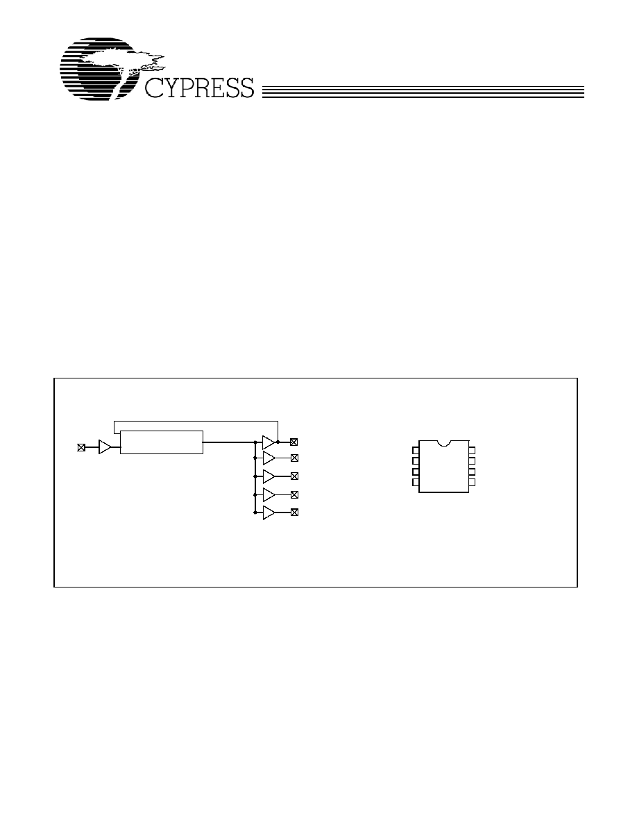
Block Diagram
Pin Configuration
1
2
3
4
5
8
7
6
REF
CLK2
CLK1
GND
V
DD
CLKOUT
CLK4
CLK3
Top View
PLL
REF
CLK1
CLK2
CLK3
CLK4
CLKOUT
PRELIMINARY
CY23EP05
Document #: 38-07759 Rev. **
Page 2 of 11
Zero Delay and Skew Control
All outputs should be uniformly loaded to achieve Zero Delay
between the input and output. Since the CLKOUT pin is the
internal feedback to the PLL, its relative loading can adjust the
input-output delay.
The output driving the CLKOUT pin will be driving a total load
of 5 pF plus any additional load externally connected to this
pin. For applications requiring zero input-output delay, the total
load on each output pin (including CLKOUT) must be the
same. If input-output delay adjustments are required, the
CLKOUT load may be changed to vary the delay between the
REF input and remaining outputs.
For zero output-output skew, be sure to load all outputs
equally. For further information refer to the application note
titled "CY2305 and CY2309 as PCI and SDRAM Buffers".
Notes:
1. Weak pull-down.
2. Weak pull-down on all outputs.
3. This output is driven and has an internal feedback for the PLL. The load on this output can be adjusted to change the skew between the reference and output.
Pin Description
Pin
Signal
Description
1
REF
[1]
Input reference frequency
2
CLK2
[2]
Buffered clock output
3
CLK1
[2]
Buffered clock output
4
GND
Ground
5
CLK3
[2]
Buffered clock output
6
V
DD
3.3V or 2.5V supply
7
CLK4
[2]
Buffered clock output
8
CLKOUT
[2,3]
Buffered clock output, internal feedback on this pin
PRELIMINARY
CY23EP05
Document #: 38-07759 Rev. **
Page 3 of 11
Absolute Maximum Conditions
Supply Voltage to Ground Potential ................. ≠0.5V to 4.6V
DC Input Voltage ...................................... V
SS
≠ 0.5V to 4.6V
Storage Temperature .................................... ≠65∞C to 150∞C
Junction Temperature .................................................. 150∞C
Static Discharge Voltage
(per MIL-STD-883, Method 3015..............................> 2000V
Operating Conditions
Parameter
Description
Min.
Max.
Unit
V
DD3.3
3.3V Supply Voltage
3.0
3.6
V
V
DD2.5
2.5V Supply Voltage
2.3
2.7
V
T
A
Operating Temperature (Ambient Temperature)--Commercial
0
70
∞C
Operating Temperature (Ambient Temperature)--Industrial
≠40
85
∞C
C
L
[4]
Load Capacitance, <100 MHz, 3.3V
≠
30
pF
Load Capacitance, <100 MHz, 2.5V with High drive
≠
30
pF
Load Capacitance, <133.3 MHz, 3.3V
≠
22
pF
Load Capacitance, <133.3 MHz, 2.5V with High drive
≠
22
pF
Load Capacitance, <133.3 MHz, 2.5V with Standard drive
≠
15
pF
Load Capacitance, >133.3 MHz, 3.3V
≠
15
pF
Load Capacitance, >133.3 MHz, 2.5V with High drive
≠
15
pF
C
IN
Input Capacitance
[5]
≠
5
pF
BW
Closed-loop bandwidth (typical), 3.3V
1≠1.5
MHz
Closed-loop bandwidth (typical), 2.5V
0.8
MHz
R
OUT
Output Impedance (typical), 3.3V High drive
29
Output Impedance (typical), 3.3V Standard drive
41
Output Impedance (typical), 2.5V High drive
37
Output Impedance (typical), 2.5V Standard drive
41
t
PU
Power-up time for all VDD's to reach minimum specified voltage
(power ramps must be monotonic)
0.01
50
ms
Theta Ja
[6]
Dissipation, Junction to Ambient, 8-pin SOIC
131
∞C/W
Theta Jc
[6]
Dissipation, Junction to Case, 8-pin SOIC
81
∞C/W
3.3V DC Electrical Specifications
Parameter
Description
Test Conditions
Min.
Max.
Unit
V
DD
Supply Voltage
3.0
3.6
V
V
IL
Input LOW Voltage
≠
0.8
V
V
IH
Input HIGH Voltage
2.0
V
DD
+ 0.3
V
I
IL
Input Leakage Current
0 < V
IN
< V
IL
≠
±10
µA
I
IH
Input HIGH Current
V
IN
= V
DD
≠
100
µA
V
OL
Output LOW Voltage
I
OL
= 8 mA (standard drive)
I
OL
= 12 mA (High drive)
≠
≠
0.4
0.4
V
V
V
OH
Output HIGH Voltage
I
OH
= ≠8 mA (standard drive)
I
OH
= ≠12 mA (High drive)
2.4
2.4
≠
≠
V
V
I
DD
(PD mode)
Power Down Supply Current REF = 0 MHz (Commercial)
≠
12
µA
REF = 0 MHz (Industrial)
≠
25
µA
I
DD
Supply Current
Unloaded outputs, 66-MHz REF
≠
30
mA
Notes:
4. Applies to Test Circuit #1
5. Applies to both REF Clock and internal feedback path on CLKOUT
6. Theta Ja, EIA JEDEC 51 test board conditions, 2S2P; Theta Jc Mil-Spec 883E Method 1012.1
PRELIMINARY
CY23EP05
Document #: 38-07759 Rev. **
Page 4 of 11
2.5V DC Electrical Specifications
Parameter
Description
Test Conditions
Min.
Max.
Unit
V
DD
Supply Voltage
2.3
2.7
V
V
IL
Input LOW Voltage
≠
0.7
V
V
IH
Input HIGH Voltage
1.7
V
DD
+ 0.3
V
I
IL
Input Leakage Current
0<V
IN
< V
DD
≠
10
µA
I
IH
Input HIGH Current
V
IN
= V
DD
≠
100
µA
V
OL
Output LOW Voltage
I
OL
= 8 mA (Standard drive)
I
OL
= 12 mA (High drive)
≠
≠
0.5
0.5
V
V
V
OH
Output HIGH Voltage
I
OH
= ≠8 mA (Standard drive)
I
OH
= ≠12 mA (High drive)
V
DD
≠ 0.6
V
DD
≠ 0.6
≠
≠
V
V
I
DD
(PD mode)
Power Down Supply Current REF = 0 MHz (Commercial)
≠
12
µA
REF = 0 MHz (Industrial)
≠
25
µA
I
DD
Supply Current
Unloaded outputs, 66-MHz REF
≠
45
mA
3.3V and 2.5V AC Electrical Specifications
Parameter
Description
Test Conditions
Min.
Typ.
Max.
Unit
1/t
1
Maximum Frequency
[7]
(Input/Output)
3.3V High drive
10
≠
220
MHz
3.3V Standard drive
10
≠
167
MHz
2.5V High drive
10
≠
200
MHz
2.5V Standard drive
10
≠
133
MHz
T
IDC
Input Duty Cycle
<133.3 MHz
25
≠
75
%
>133.3 MHz
40
≠
60
%
t
2
˜ t
1
Output Duty Cycle
[8]
<133.3 MHz
47
≠
53
%
>133.3 MHz
45
≠
55
%
t
3,
t
4
Rise, Fall Time (3.3V)
[8]
Std drive, CL = 30 pF, <100 MHz
≠
≠
1.6
ns
Std drive, CL = 22 pF, <133.3 MHz
≠
≠
1.6
ns
Std drive, CL = 15 pF, <167 MHz
≠
≠
0.6
ns
High drive, CL = 30 pF, <100 MHz
≠
≠
1.2
ns
High drive, CL = 22 pF, <133.3 MHz
≠
≠
1.2
ns
High drive, CL = 15 pF, >133.3 MHz
≠
≠
0.5
ns
t
3,
t
4
Rise, Fall Time (2.5V)
[8]
Std drive, CL = 15 pF, <133.33 MHz
≠
≠
1.5
ns
High drive, CL = 30 pF, <100 MHz
≠
≠
2.1
ns
High drive, CL = 22 pF, <133.3 MHz
≠
≠
1.3
ns
High drive, CL = 15 pF, >133.3 MHz
≠
≠
1.2
ns
t
5
Output to Output Skew
[8]
All outputs equally loaded
≠
30
100
ps
t
6
Delay, REF Rising Edge to
CLKOUT Rising Edge
[8]
PLL enabled @ 3.3V
≠100
≠
100
ps
PLL enabled @2.5V
≠200
≠
200
ps
t
7
Part to Part Skew
[8]
Measured at V
DD
/2.
Any output to any output, 3.3V supply
≠
≠
±150
ps
Measured at V
DD
/2.
Any output to any output, 2.5V supply
≠
≠
±300
ps
Notes:
7. For the given maximum loading conditions. See C
L
in Operating Conditions Table
8. Parameter is guaranteed by design and characterization. Not 100% tested in production
PRELIMINARY
CY23EP05
Document #: 38-07759 Rev. **
Page 5 of 11
t
LOCK
PLL Lock Time
[8]
Stable power supply, valid clocks presented on
REF and CLKOUT pins
≠
≠
1.0
ms
T
JCC
[8,9]
Cycle-to-cycle Jitter, Peak 3.3V supply, >66 MHz, <15 pF
≠
22
55
ps
3.3V supply, >66 MHz, <30 pF, standard drive
≠
45
125
ps
3.3V supply, >66 MHz, <30 pF, high drive
≠
45
100
ps
2.5V supply, >66 MHz, <15 pF, standard drive
≠
40
100
ps
2.5V supply, >66 MHz, <15 pF, high drive
≠
35
80
ps
2.5V supply, >66 MHz, <30 pF, high drive
≠
52
125
ps
T
PER
[8,9]
Period Jitter, Peak
3.3V supply, 66≠100 MHz, <15 pF
≠
18
60
ps
3.3V supply, >100 MHz, <15 pF
≠
13
35
ps
3.3V supply, >66 MHz, <30 pF, standard drive
≠
28
75
ps
3.3V supply, >66 MHz, <30 pF, high drive
≠
26
70
ps
2.5V supply, >66 MHz, <15 pF, standard drive
≠
25
60
ps
2.5V supply, 66≠100 MHz, <15 pF, high drive
≠
22
60
ps
2.5V supply, >100 MHz, <15 pF, high drive
≠
19
45
ps
3.3V and 2.5V AC Electrical Specifications
(continued)
Parameter
Description
Test Conditions
Min.
Typ.
Max.
Unit
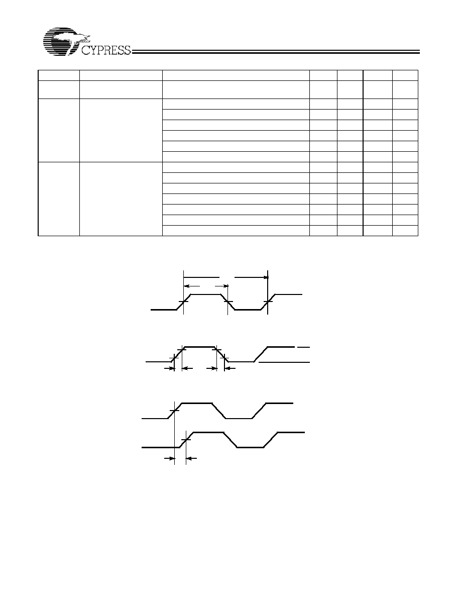
Switching Waveforms
Note:
9. As defined by JESD65B. Typical jitter is measured at 3.3V or 2.5V, 29∞C, with all outputs driven into the maximum specified load.
Duty Cycle Timing
t
1
t
2
V
DD
/2
V
DD
/2
V
DD
/2
All Outputs Rise/Fall Time
OUTPUT
t
3
3.3V(2.5V)
0V
0.8V(0.6V)
2.0V(1.8V)
2.0V(1.8V)
0.8V(0.6V)
t
4
Output-Output Skew
t
5
OUTPUT
OUTPUT
V
DD
/2
V
DD
/2
PRELIMINARY
CY23EP05
Document #: 38-07759 Rev. **
Page 6 of 11
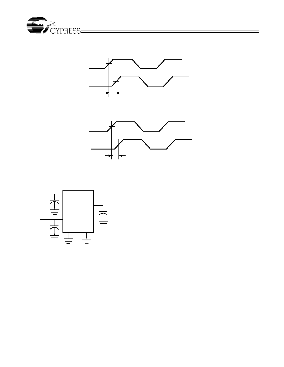
Switching Waveforms
(continued)
Input-Output Propagation Delay
V
DD
/2
t
6
INPUT
FBK
V
DD
/2
V
DD
/2
V
DD
/2
t
7
Any output, Part 1 or 2
Any output, Part 1 or 2
Part-Part Skew
Test Circuits
0.1
µ F
V DD
0.1
µ F
V DD
CLK
C LOAD
OUTPUTS
GND
GND
Test Circuit # 1
PRELIMINARY
CY23EP05
Document #: 38-07759 Rev. **
Page 7 of 11
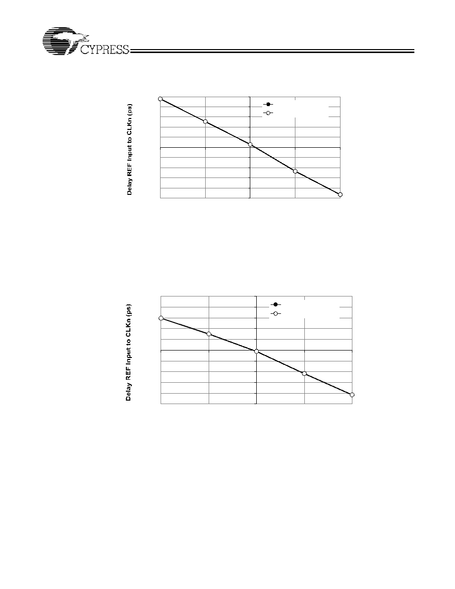
Supplemental Parametric Information
Figure 1. 2.5V typical room temperature graph for REF Input to CLKn delay versus loading difference between
CLKOUT and CLKn. Data is shown for 66 MHz. Delay is a weak function of frequency.
-1000
-800
-600
-400
-200
0
200
400
600
800
1000
-20
-10
0
10
20
Load CLKOUT- Load CLKn (pF)
2.5V Standard Drive
2.5V High Drive
Figure 2. 3.3V typical room temperature graph for REF Input to CLKn delay versus loading difference between
CLKOUT and CLKn. Data is shown for 66 MHz. Delay is a weak function of frequency.
-1000
-800
-600
-400
-200
0
200
400
600
800
1000
-20
-10
0
10
20
Load CLKOUT- Load CLKn (pF)
3.3V Standard Drive
3.3V High Drive
PRELIMINARY
CY23EP05
Document #: 38-07759 Rev. **
Page 8 of 11
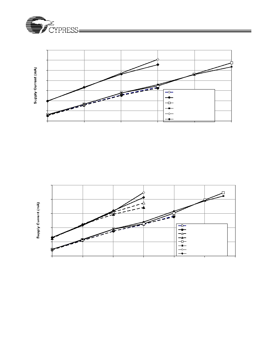
Figure 3. 2.7V measured supply current versus frequency, drive strength, loading, and temperature. Note that the
30-pF data above 100 MHz is beyond the data sheet specification of 22 pF.
0
10
20
30
40
50
60
70
33
66
100
133
166
200
Frequency (MHz)
15pF, -45C, Standard Drive
15pF, 90C, Standard Drive
15pF, -45C, High Drive
15pF, 90C, High Drive
30pF, -45C, High Drive
30pF, 90C, High Drive
Figure 4. 3.6V measured supply current versus frequency, drive strength, loading, and temperature. Note that
the 30-pF high-drive data above 100 MHz is beyond the data sheet specification of 22 pF.
0
20
40
60
80
100
33
66
100
133
166
200
233
Frequency (MHz)
15pF, -45C, Standard Drive
15pF, 90C, Standard Drive
30pF, -45C, Standard Drive
30pF, 90C, Standard Drive
15pF, -45C, High Drive
15pF, 90C, High Drive
30pF, -45C, High Drive
30pF, 90C, High Drive
PRELIMINARY
CY23EP05
Document #: 38-07759 Rev. **
Page 9 of 11
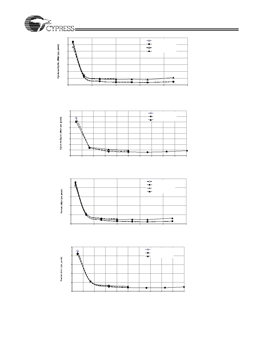
Figure 5. Typical 3.3V measured cycle-to-cycle jitter at 29∞C, versus frequency, drive strength, and loading
0
50
100
150
200
250
300
350
0
50
100
150
200
250
Frequency (MHz)
15 pF, Standard Drive
15 pF, High Drive
30 pF, Standard Drive
30 pF, High Drive
Figure 6. Typical 2.5V measured cycle-to-cycle jitter at 29∞C, versus frequency, drive strength, and loading
0
50
100
150
200
250
300
350
400
0
20
40
60
80
100
120
140
160
180
200
Frequency (MHz)
15 pF, Standard Drive
15 pF, High Drive
30 pF, High Drive
Figure 7. Typical 3.3V measured period jitter at 29∞C, versus frequency, drive strength, and loading.
0
50
100
150
200
250
0
50
100
150
200
250
Frequency (MHz)
15 pF, Standard Drive
15 pF, High Drive
30 pF, Standard Drive
30 pF, High Drive
Figure 8. Typical 2.5V measured period jitter at 29∞C, versus frequency, drive strength, and loading
0
50
100
150
200
250
0
20
40
60
80
100
120
140
160
180
200
Frequency (MHz)
15 pF, Standard Drive
15 pF, High Drive
30 pF, High Drive
PRELIMINARY
CY23EP05
Document #: 38-07759 Rev. **
Page 10 of 11
© Cypress Semiconductor Corporation, 2005. The information contained herein is subject to change without notice. Cypress Semiconductor Corporation assumes no responsibility for the use
of any circuitry other than circuitry embodied in a Cypress product. Nor does it convey or imply any license under patent or other rights. Cypress products are not warranted nor intended to be
used for medical, life support, life saving, critical control or safety applications, unless pursuant to an express written agreement with Cypress. Furthermore, Cypress does not authorize its
products for use as critical components in life-support systems where a malfunction or failure may reasonably be expected to result in significant injury to the user. The inclusion of Cypress
products in life-support systems application implies that the manufacturer assumes all risk of such use and in doing so indemnifies Cypress against all charges.
All product and company names mentioned in this document may be the trademarks of their respective holders.
Ordering Information
Ordering Code
Package Type
Operating Range
Lead-free
CY23EP05SXC-1
8-pin 150-mil SOIC
Commercial
CY23EP05SXC-T
8-pin 150-mil SOIC ≠ Tape and Reel
Commercial
CY23EP05SXI-1
8-pin 150-mil SOIC
Industrial
CY23EP05SXI-1T
8-pin 150-mil SOIC ≠ Tape and Reel
Industrial
CY23EP05SXC-1H
8-pin 150-mil SOIC
Commercial
CY23EP05SXC-1HT
8-pin 150-mil SOIC ≠ Tape and Reel
Commercial
CY23EP05SXI-1H
8-pin 150-mil SOIC
Industrial
CY23EP05SXI-1HT
8-pin 150-mil SOIC ≠ Tape and Reel
Industrial
Package Drawing and Dimensions
SEATING PLANE
PIN 1 ID
0.230[5.842]
0.244[6.197]
0.157[3.987]
0.150[3.810]
0.189[4.800]
0.196[4.978]
0.050[1.270]
BSC
0.061[1.549]
0.068[1.727]
0.004[0.102]
0.0098[0.249]
0.0138[0.350]
0.0192[0.487]
0.016[0.406]
0.035[0.889]
0.0075[0.190]
0.0098[0.249]
1. DIMENSIONS IN INCHES[MM] MIN.
MAX.
0∞~8∞
0.016[0.406]
0.010[0.254]
X 45∞
2. PIN 1 ID IS OPTIONAL,
ROUND ON SINGLE LEADFRAME
RECTANGULAR ON MATRIX LEADFRAME
0.004[0.102]
8 Lead (150 Mil) SOIC - S08
1
4
5
8
3. REFERENCE JEDEC MS-012
PART #
S08.15 STANDARD PKG.
SZ08.15 LEAD FREE PKG.
4. PACKAGE WEIGHT 0.07gms
51-85066-*C
8-lead (150-Mil) SOIC S8

PRELIMINARY
CY23EP05
Document #: 38-07759 Rev. **
Page 11 of 11
Document History Page
Document Title: CY23EP05 2.5V or 3.3V, 10-220-MHz, Low Jitter, 5 Output Zero Delay Buffer
Document Number: 38-07759
REV.
ECN NO. Issue Date
Orig. of
Change
Description of Change
**
349620
See ECN
RGL
New data sheet