MPEG Clock Generator with VCXO
CY2412
Cypress Semiconductor Corporation
∑
3901 North First Street
∑
San Jose
,
CA 95134
∑
408-943-2600
Document #: 38-07227 Rev. *D
Revised December 13, 2004
Features
∑ Integrated phase-locked loop (PLL)
∑ Low-jitter, high-accuracy outputs
∑ VCXO with analog adjust
∑ 3.3V operation
∑ 8-pin SOIC package
Benefits
∑ Highest-performance PLL tailored for multimedia appli-
cations
∑ Meets critical timing requirements in complex system
designs
∑ Large ± 150-ppm range, better linearity
∑ Enables application compatibility
Part Number
Outputs
Input Frequency Range
Output Frequencies
VCXO Profile
CY2412-1
3
13.5-MHz pullable crystal input per
Cypress specification
Two 27 MHz outputs, one 54 MHz (3.3V) Linear
CY2412-3
3
13.5-MHz pullable crystal input per
Cypress specification
27 MHz, 13.5 MHz, 54 MHz (3.3V)
Linear
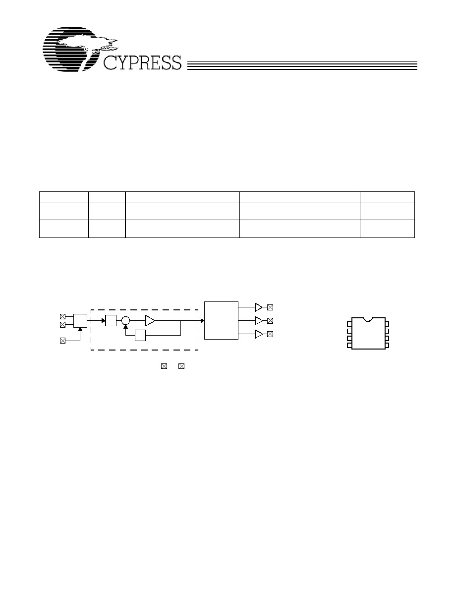
Logic Block Diagram
13.5 XIN
XOUT
CLKC
OUTPUT
DIVIDERS
PLL
OSC
VCXO
CLKA
Q
P
VCO
VDD
VSS
CLKB
8-pin SOIC
CY2412-1,-3
1
2
3
4
XOUT
XIN
VCXO
CLKA
VSS
CLKC
CLKB
5
6
7
8
VDD
Pin Configuration
CY2412
Document #: 38-07227 Rev. *D
Page 2 of 6
Note:
1. Crystals that meet this specification includes: Ecliptek ECX-5788-13.500M,Siward XTL001050A-13.5-14-400, Raltron A-13.500-14-CL,PDI HA13500XFSA14XC.
Pin Summary
Pin Name
Pin Number
Pin Description
X
IN
1
Reference Crystal Input
V
DD
2
Voltage Supply
VCXO
3
Input Analog Control for VCXO
V
SS
4
Ground
CLKA
5
54-MHz clock output
CLKB
6
13.5-MHz clock output
CLKC
7
27-MHz clock output
X
OUT
[2]
8
Reference Crystal Output
Pullable Crystal Specifications
[1]
Parameter
Description
Condition
Min.
Typ.
Max. Unit
F
NOM
Nominal crystal frequency
Parallel resonance, funda-
mental mode, AT cut
≠
13.5
≠
MHz
C
LNOM
Nominal load capacitance
≠
14
≠
pF
R
1
Equivalent series resistance (ESR)
Fundamental mode
≠
≠
25
R
3
/R
1
Ratio of third overtone mode ESR to funda-
mental mode ESR
Ratio used because typical R
1
values are much less than the
maximum spec.
3
≠
≠
DL
Crystal drive level
No external series resistor as-
sumed
≠
0.5
2.0
mW
F
3SEPHI
Third overtone separation from 3*F
NOM
High side
300
≠
≠
ppm
F
3SEPLO
Third overtone separation from 3*F
NOM
Low side
≠
≠
≠150 ppm
C
0
Crystal shunt capacitance
≠
≠
7
pF
C
0/
C
1
Ratio of shunt to motional capacitance
180
≠
250
C
1
Crystal motional capacitance
14.4
18
21.6
pF
CY2412
Document #: 38-07227 Rev. *D
Page 3 of 6
Absolute Maximum Conditions
Recommended Operating Conditions
DC Electrical Characteristics
AC Electrical Characteristics
Parameter
Description
Min.
Max.
Unit
V
DD
Supply Voltage
≠0.5
7.0
V
T
S
Storage Temperature
[3]
≠65
125
∞C
T
J
Junction Temperature
≠
125
∞C
Digital Inputs
V
SS
≠ 0.3
V
DD
+ 0.3
V
Digital Outputs referred to V
DD
V
SS
≠ 0.3
V
DD
+ 0.3
V
Electrostatic Discharge
2
kV
Parameter
Description
Min.
Typ.
Max.
Unit
V
DD
Operating Voltage
3.14
3.3
3.47
V
T
A
Ambient Temperature
0
70
∞C
C
LOAD
Max. Load Capacitance
15
pF
f
REF
Reference Frequency
13.5
MHz
t
PU
Power-up time for all VDDs to reach
minimum specified voltage (power
ramps must be monotonic)
0.05
500
ms
Parameter
Description
Test Conditions
Min.
Typ.
Max.
Unit
I
OH
Output High Current
V
OH
= V
DD
≠ 0.5, V
DD
= 3.3V
12
24
mA
I
OL
Output Low Current
V
OL
= 0.5, V
DD
= 3.3V
12
24
mA
C
IN
Input Capacitance
7
pF
I
IZ
Input Leakage Current
5
µA
f
XO
VCXO pullability range
+150
ppm
V
VCXO
VCXO input range
0
V
DD
V
f
VBW
VCXO input bandwidth
DC to 200
kHz
I
DD
Supply Current
Sum of Core and Output Current
35
mA
Parameter
[4]
Description
Test Conditions
Min.
Typ.
Max.
Unit
DC
Output Duty Cycle
Duty Cycle is defined in Figure 1, 50% of V
DD
45
50
55
%
ER
Rising Edge Rate
Clock Edge Rate, Measured from 20% to 80%
of V
DD,
C
LOAD
= 15 pF. See Figure 2.
0.8
1.4
V/ns
EF
Falling Edge Rate
Output Clock Edge Rate, Measured from 80% to
20% of V
DD,
C
LOAD
= 15 pF. See Figure 2.
0.8
1.4
V/ns
t
9
Clock Jitter
Peak to Peak period jitter
100
200
ps
t
10
PLL Lock Time
3
ms
Notes:
2. Float X
OUT
if X
IN
is externally driven.
3. Rated for ten years.
4. Not 100% tested.
CY2412
Document #: 38-07227 Rev. *D
Page 4 of 6
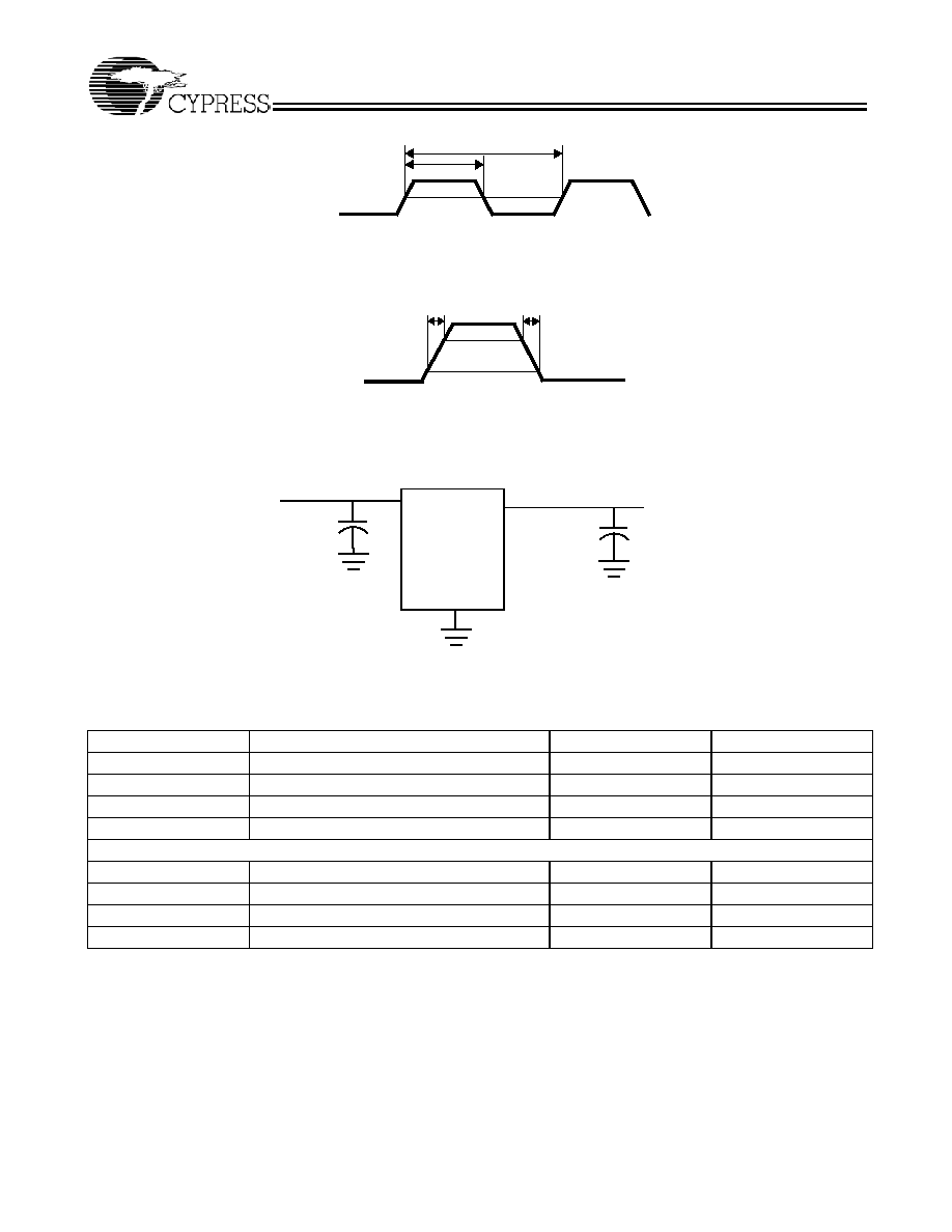
t1
t2
CLK
50%
50%
Figure 1. Duty Cycle Definition; DC = t2/t1
t3
CLK
80%
20%
t4
Figure 2. Rise and Fall Time Definitions: ER = 0.6 x VDD / t3 , EF = 0.6 x VDD / t4
Test Circuit
0.1
µF
V
DD
CLK out
C
LOAD
GND
OUTPUTS
Ordering Information
Ordering Code
Package Type
Operating Range
Operating Voltage
CY2412SC-1
8-pin SOIC
Commercial
3.3V
CY2412SC-1T
8-pin SOIC≠Tape and Reel
Commercial
3.3V
CY2412SC-3
8-pin SOIC
Commercial
3.3V
CY2412SC-3T
8-pin SOIC≠Tape and Reel
Commercial
3.3V
Lead-free
CY2412SXC-1
8-pin SOIC
Commercial
3.3V
CY2412SXC-1T
8-pin SOIC≠Tape and Reel
Commercial
3.3V
CY2412SXC-3
8-pin SOIC
Commercial
3.3V
CY2412SXC-3T
8-pin SOIC≠Tape and Reel
Commercial
3.3V
CY2412
Document #: 38-07227 Rev. *D
Page 5 of 6
© Cypress Semiconductor Corporation, 2004. The information contained herein is subject to change without notice. Cypress Semiconductor Corporation assumes no responsibility for the use
of any circuitry other than circuitry embodied in a Cypress product. Nor does it convey or imply any license under patent or other rights. Cypress products are not warranted nor intended to be
used for medical, life support, life saving, critical control or safety applications, unless pursuant to an express written agreement with Cypress. Furthermore, Cypress does not authorize its
products for use as critical components in life-support systems where a malfunction or failure may reasonably be expected to result in significant injury to the user. The inclusion of Cypress
products in life-support systems application implies that the manufacturer assumes all risk of such use and in doing so indemnifies Cypress against all charges.
Package Diagram
All products and company names mentioned in this document may be the trademarks of their respective holders.
SEATING PLANE
PIN 1 ID
0.230[5.842]
0.244[6.197]
0.157[3.987]
0.150[3.810]
0.189[4.800]
0.196[4.978]
0.050[1.270]
BSC
0.061[1.549]
0.068[1.727]
0.004[0.102]
0.0098[0.249]
0.0138[0.350]
0.0192[0.487]
0.016[0.406]
0.035[0.889]
0.0075[0.190]
0.0098[0.249]
1. DIMENSIONS IN INCHES[MM] MIN.
MAX.
0∞~8∞
0.016[0.406]
0.010[0.254]
X 45∞
2. PIN 1 ID IS OPTIONAL,
ROUND ON SINGLE LEADFRAME
RECTANGULAR ON MATRIX LEADFRAME
0.004[0.102]
8 Lead (150 Mil) SOIC S08
1
4
5
8
3. REFERENCE JEDEC MS-012
PART #
S08.15 STANDARD PKG.
SZ08.15 LEAD FREE PKG.
4. PACKAGE WEIGHT 0.07gms
51-85066-*C
8-lead (150-Mil) SOIC S8
CY2412
Document #: 38-07227 Rev. *D
Page 6 of 6
Document History Page
Document Title: CY2412 MPEG Clock Generator with VCXO
Document Number: 38-07227
REV.
ECN NO.
Issue Date
Orig. of
Change
Description of Change
**
110492
10/28/01
SZV
Change from Spec number: 38-00898 to 38-07227
*A
112457
03/14/02
CKN
Added CY2412-2 to data sheet
*B
116961
08/06/02
CKN
Removed CY2412-2 from the datasheet. Added CY2412-3 to data sheet
*C
121879
12/14/02
RBI
Power-up requirements added to Operating Conditions Information
*D
299735
See ECN
RGL
Added lead-free for CY2412-1 and CY2412-3 devices