Äîêóìåíòàöèÿ è îïèñàíèÿ www.docs.chipfind.ru
Clock Synthesizer with Differential CPU Outputs
CY28408
Cypress Semiconductor Corporation
·
3901 North First Street
·
San Jose
,
CA 95134
·
408-943-2600
Document #: 38-07617 Rev. **
Revised December 17, 2003
Features
· Compatible to Intel
®
CK 408 Mobile Clock Synthesizer
· Support Intel P4 and Brookdale CPU
· Specifications
· 3.3V power supply
· Three differential CPU clocks
· Ten copies of PCI clocks
· Six copies of 3V66 clocks
· SMBus support with read back capabilities
· Spread Spectrum electromagnetic interference (EMI)
reduction
· Dial-A-Frequency
®
features
· Dial-A-dB
features
· 56-pin TSSOP package
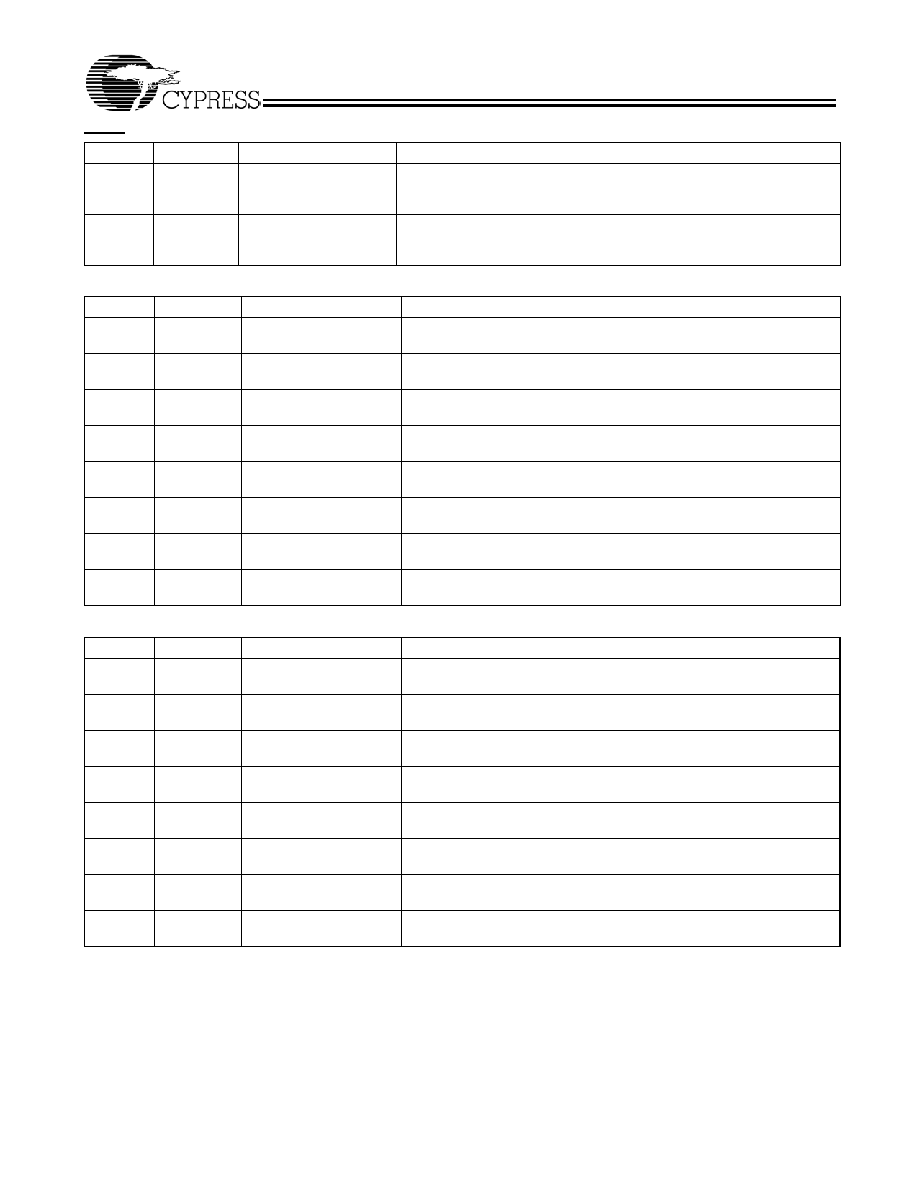
Note:
1. TCLK is a test clock driven on the XTAL_IN input during test mode. M = driven to a level between 1.0V and 1.8V. If the S2 pin is at a M level during power-up, an
0 state will be latched into the device's internal state register.
Table 1. Frequency Table
[1]
S2 S1
S0
CPU(0:2)
3V66
PCI_PCIF
REF
USB/DOT
1
0
0
100 MHz
66 MHz
33 MHz
14.318 MHz
48 MHz
1
0
1
133 MHz
66 MHz
33 MHz
14.318 MHz
48 MHz
1
1
0
Reserved
1
1
1
166 MHz
66 MHz
33 MHz
14.318 MHz
48 MHz
0
0
0
66 MHz
66 MHz
33 MHz
14.318 MHz
48 MHz
0
0
1
100 MHz
66 MHz
33 MHz
14.318 MHz
48 MHz
0
1
0
Reserved
0
1
1
133 MHz
66 MHz
33 MHz
14.318 MHz
48 MHz
M
0
0
Hi-Z
Hi-Z
Hi-Z
Hi-Z
Hi-Z
M
0
1
TCLK/2
TCLK/4
TCLK/8
TCLK
TCLK/2
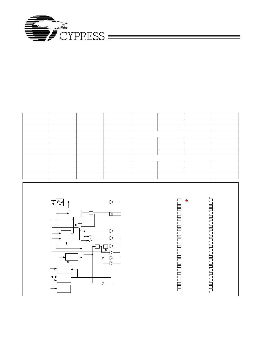
Block Diagram
Pin Configuration
PLL1
PLL2
/2
WD
Logic
Power
Up Logic
XIN
XOUT
CPU_STP#
IREF
VSSIREF
S(0:2)
MULT0
VTT_PWRGD#
PCI_STP#
PD#
SDATA
SCLK
VDDA
3V66[2:5]
48M_DOT
48M_USB
PCI_F(0:2)
PCI(0:6)
3V66_1/VCH
3V66_0
CPUC(0:2)
CPUT(0:2)
REF
I2C
Logic
VDD
XIN
XOUT
VSS
PCIF0
PCIF1
PCIF2
VDD
VSS
PCI0
EPCI1/PCI1
PCI2
EPCI3/PCI3
VDD
VSS
PCI4
PCI5
PCI6
VDD
VSS
3V66_2
3V66_3
3V66_4
3V66_5
PD#
VDDA
VSSA
VTT_PWRGD#
REF
S1
S0
CPU_STP#
CPUT0
CPUC0
VDD
CPUT1
CPUC1
VSS
VDD
CPUT2
CPUC2
MULT0
IREF
VSSIREF
S2
48M_USB
48M_DOT
VDD
VSS
3V66_1/VCH
PCI_STP#
3V66_0
VDD
VSS
SCLK
SDATA
1
2
3
4
5
6
7
8
9
10
11
12
13
14
15
16
17
18
19
20
21
22
23
24
25
26
27
28
56
55
54
53
52
51
50
49
48
47
46
45
44
43
42
41
40
39
38
37
36
35
34
33
32
31
30
29
C
Y
2
8408
CY28408
Document #: 38-07617 Rev. **
Page 2 of 19
Pin Description
Pin
Name
PWR
I/O
Description
2
XIN
VDD
I
Oscillator buffer input. Connect to a crystal or to an external clock.
3
XOUT
VDD
O
Oscillator buffer output. Connect to a crystal. Do not connect when an
external clock is applied at XIN.
52, 51, 49, 48,
45, 44
CPUT(0:2),
CPUC(0:2)
VDD
O
Differential host output clock pairs. See Table 1 for frequencies and
functionality.
10, 12, 16, 17, 18 PCI(0,2)/(3:5)
VDDP
O
PCI clock outputs. Synchronous to the 3V66 clock. See Table 1.
11,13
EPCI/PCI(1,3)
VDD
I/O
PD
Early or normal PCI clock outputs. There is an internal 250k
pull-down resistor. See Table 8.
5, 6, 7
PCIF (0:2)
VDD
O
33-MHz PCI clocks, which are
÷2 copies of 3V66 clocks, may be free running
(not stopped when PCI_STP# is asserted LOW) or may be stoppable
depending on the programming of SMBus register Byte3, Bits (3:5).
56
REF
VDD
O
Buffered output copy of the device's XIN clock.
42
IREF
VDD
I
Current reference programming input for CPU buffers. A resistor is
connected between this pin and VSSIREF.
28
VTT_PWRGD#
VDD
I
Qualifying input that latches S(0:2) and MULT0. When this input is at
a logic low, the S(0:2) and MULT0 are latched
39
48M_USB
VDD48
O
Fixed 48-MHz USB clock outputs.
38
48M_DOT
VDD48
O
Fixed 48-MHZ DOT clock outputs.
33
3V66_0
VDD
O
3.3V 66-MHz fixed frequency clock.
35
3V66_1/VCH
VDD
O
3.3V clock selectable with SMBus byte0, Bit5, when Byte5, Bit5.
When Byte 0 Bit 5 is at a logic 1, then this pin is a 48M output clock. When
byte0, Bit5 is a logic 0, then this is a 66-MHz output clock (default).
21, 22, 23, 24
3V66(2:5)
VDD
O
3.3V 66-MHz fixed frequency clock.
25
PD#
VDD
I
PU
This pin is a power-down mode pin. A logic LOW level causes the
device to enter a power-down state. All internal logic is turned off except
for the SMBus logic. All output buffers are stopped.
43
MULT0
VDD
I
PU
Programming input selection for CPU clock current multiplier.
0 = 4 * IREF, 1 = 6 * =IREF
55, 54
S(0,1)
VDD
I
Frequency select inputs. See Table 1
29
SDATA
VDD
I/O
PU
Serial data input. Conforms to the SMBus specification of a Slave
Receive/Transmit device. It is an input when receiving data. It is an open
drain output when acknowledging or transmitting data.
30
SCLK
VDD
I
PU
Serial clock input. Conforms to the SMBus specification.
40
S2
VDD
I
T
Frequency select input. See Table 1. This is a tri-level input that is
driven HIGH, LOW, or driven to a intermediate level.
34
PCI_STP#
VDD
I
PU
PCI clock disable input. When asserted LOW, PCI (0:6) clocks are
synchronously disabled in a LOW state. This pin does not effect PCIF
(0:2) clock outputs if they are programmed to be PCIF clocks via the
device's SMBus interface.
53
CPU_STP#
VDD
I
PU
CPU clock disable input. When asserted LOW, CPUT (0:2) clocks are
synchronously disabled in a HIGH state and CPUC(0:2) clocks are
synchronously disabled in a LOW state.
1, 8, 14, 19, 32,
37, 46, 50
VDD
PWR 3.3V power supply.
4, 9, 15, 20, 27,
31, 36, 47
VSS
PWR Common ground.
41
VSSIREF
PWR Current reference programming input for CPU buffers. A resistor is
connected between this pin and IREF. This pin should also be returned
to device VSS.
26
VDDA
PWR Analog power input. Used for PLL and internal analog circuits. It is also
specifically used to detect and determine when power is at an acceptable
level to enable the device to operate.
CY28408
Document #: 38-07617 Rev. **
Page 3 of 19
Serial Data Interface
To enhance the flexibility and function of the clock synthesizer,
a two-signal serial interface is provided. Through the Serial
Data Interface, various device functions, such as individual
clock output buffers, can be individually enabled or disabled.
The registers associated with the Serial Data Interface
initializes to their default setting upon power-up, and therefore
use of this interface is optional. Clock device register changes
are normally made upon system initialization, if any are
required. The interface can also be used during system
operation for power management functions.
Data Protocol
The clock driver serial protocol accepts block write and block
read operations from the controller. For block write/read
operation, the bytes must be accessed in sequential order
from lowest to highest byte (most significant bit first) with the
ability to stop after any complete byte has been transferred.
The block write and block read protocol is outlined in Table 3
while Table 4 outlines the corresponding byte write and byte
read protocol. The slave receiver address is 11010010 (D2h).
Table 2. Command Code Definition
Bit
Description
7
0 = Block read or block write operation, 1 = Byte read or byte write operation
(6:0)
Byte offset for byte read or byte write operation. For block read or block write operations, these bits should be
'0000000'
Table 3. Block Read and Block Write Protocol
Block Write Protocol
Block Read Protocol
Bit
Description
Bit
Description
1
Start
1
Start
8:2
Slave address 7 bits
8:2
Slave address 7 bits
9
Write 9
Write
10
Acknowledge from slave
10
Acknowledge from slave
18:11
Command Code 8 Bits
18:11
Command Code 8 Bits
19
Acknowledge from slave
19
Acknowledge from slave
27:20
Byte Count 8 bits
(Skip this step if I
2
C_EN bit set)
20
Repeat start
28
Acknowledge from slave
27:21
Slave address 7 bits
36:29
Data byte 1 8 bits
28
Read = 1
37
Acknowledge from slave
29
Acknowledge from slave
45:38
Data byte 2 8 bits
37:30
Byte Count from slave 8 bits
46
Acknowledge from slave
38
Acknowledge
....
Data Byte /Slave Acknowledges
46:39
Data byte 1 from slave 8 bits
....
Data Byte N 8 bits
47
Acknowledge
....
Acknowledge from slave
55:48
Data byte 2 from slave 8 bits
....
Stop
56
Acknowledge
....
Data bytes from slave / Acknowledge
....
Data Bte N from slave 8 bits
....
NOT Acknowledge
...
Stop
Table 4. Byte Read and Byte Write Protocol
Byte Write Protocol
Byte Read Protocol
Bit
Description
Bit
Description
1
Start
1
Start
8:2
Slave address 7 bits
8:2
Slave address 7 bits
9
Write
9
Write
10
Acknowledge from slave
10
Acknowledge from slave
18:11
Command Code 8 bits
18:11
Command Code 8 bits
CY28408
Document #: 38-07617 Rev. **
Page 4 of 19
19
Acknowledge from slave
19
Acknowledge from slave
27:20
Data byte 8 bits
20
Repeated start
28
Acknowledge from slave
27:21
Slave address 7 bits
29
Stop
28
Read
29
Acknowledge from slave
37:30
Data from slave 8 bits
38
NOT Acknowledge
39
Stop
Byte 0: CPU Clock Register
[2]
Bit
@Pup
Name
Description
7
0
Spread Spectrum Enable, 0 = Spread Off, 1 = Spread On
This is a Read and Write control bit.
6
0
CPU clock Power-down Mode Select. 0 = Drive CPUT to 4 or 6 IREF and
drive CPUC to low when PD# is asserted LOW. 1 = Three-state all CPU
outputs. This is only applicable when PD# is LOW. It is not applicable to
CPU_STP#.
5
0
3V66_1/VCH
3V66_1/VCH frequency Select, 0 = 66M selected, 1 = 48M selected
This is a Read and Write control bit.
4
Pin 53
CPU_STP#
Reflects the current value of the external CPU_STP#. This bit is Read-only.
3
Pin 34
PCI_STP#
Reflects the current value of the internal PCI_STP# function when read.
Internally PCI_STP# is a logical AND function of the internal SMBus register
bit and the external PCI_STP# pin. This is a Read and Write control bit.
2
Pin 40
SEL2
Frequency Select Bit 2. Reflects the value of SEL2. This bit is Read-only.
1
Pin 55
SEL1
Frequency Select Bit 1. Reflects the value of SEL1. This bit is Read-only.
0
Pin 54
SEL0
Frequency Select Bit 0. Reflects the value of SEL0. This bit is Read-only.
Byte 1: CPU Clock Register
Bit
@Pup
Name
Description
7
Pin 43
MULT0 Value. This bit is Read-only.
6
0
Controls functionality of CPUT/C outputs when CPU_STP# is asserted. 0
= Drive CPUT to 4 or 6 IREF and drive CPUC to low when CPU_STP# is
asserted LOW. 1 = Tri-state all CPU outputs when CPU_STP# is
asserted.This bit will override Byte0, Bit6 such that even if it is a 0, when
PD# goes low the CPU outputs will be tri-stated.
5
0
Controls CPU2 functionality when CPU_STP# is asserted LOW
1 = Free Running, 0 = Stopped LOW with CPU_STP# asserted LOW
This is a Read and Write control bit.
4
0
Controls CPU1 functionality when CPU_STP# is asserted LOW
1 = Free Running, 0 = Stopped LOW with CPU_STP# asserted LOW
This is a Read and Write control bit.
3
0
Controls CPUT0 functionality when CPU_STP# is asserted LOW
1 = Free Running, 0 = Stopped LOW with CPU_STP# asserted LOW
This is a Read and Write control bit.
2
1
CPUT/C2
CPUT/C2 Output Control
1 = enabled, 0 = three-state CPUT/C2
This is a Read and Write control bit.
Note:
2. PU = Internal Pull-up. PD = Internal Pull-down. T = Tri-level logic input.
Table 4. Byte Read and Byte Write Protocol (continued)
Byte Write Protocol
Byte Read Protocol
Bit
Description
Bit
Description
CY28408
Document #: 38-07617 Rev. **
Page 5 of 19
1
1
CPUT/C1
CPUT/C1 Output Control
1 = enabled, 0 = three-state CPUT/C1
This is a Read and Write control bit.
0
1
CPUT/C0
CPUT/C0 Output Control
1 = enabled, 0 = three-state CPUT/C0
This is a Read and Write control bit.
Byte 2: PCI Clock Control Register (all bits are read- and write-functional)
Bit
@Pup
Name
Description
7
0
REF
REF Output Control.
0 = high strength, 1 = low strength
6
1
PCI6 PCI6
Output
Control
1 = enabled, 0 = forced LOW
5
1
PCI5
PCI5 Output Control
1 = enabled, 0 = forced LOW
4
1
PCI4
PCI4 Output Control
1 = enabled, 0 = forced LOW
3
1
PCI3
PCI3 Output Control
1 = enabled, 0 = forced LOW
2
1
PCI2
PCI2 Output Control
1 = enabled, 0 = forced LOW
1
1
PCI1
PCI1 Output Control
1 = enabled, 0 = forced LOW
0
1
PCI0
PCI0 Output Control
1 = enabled, 0 = forced LOW
Byte 3: PCI_F Clock and 48M Control Register (all bits are read- and write-functional)
Bit
@Pup
Name
Description
7
1
48M_DOT 48M_DOT
Output
Control
1 = enabled, 0 = forced LOW
6
1
48M_USB
48M_USB Output Control
1 = enabled, 0 = forced LOW
5
0
PCI_STP#, control of PCI_F2.
0 = Free Running, 1 = Stopped when PCI_STP# is LOW
4
0
PCI_STP#, control of PCI_F1.
0 = Free Running, 1 = Stopped when PCI_STP# is LOW
3
0
PCI_STP#, control of PCI_F0.
0 = Free Running, 1 = Stopped when PCI_STP# is LOW
2
1
PCI_F2
PCI_F2 Output Control
1 = running, 0 = forced LOW
1
1
PCI_F1
PCI_F1 Output Control
1 = running, 0 = forced LOW
0
1
PCI_F0
PCI_F0 Output Control
1 = running, 0 = forced LOW
Byte 1: CPU Clock Register (continued)
Bit
@Pup
Name
Description