cy7c199.frm
32K x 8 Static RAM
fax id: 1030
CY7C199
Cypress Semiconductor Corporation
·
3901 North First Street
·
San Jose
·
CA 95134
·
408-943-2600
February 1988 Revised April 22, 1998
Features
· High speed
-- 10 ns
· Fast t
DOE
· CMOS for optimum speed/power
· Low active power
-- 467 mW (max, 12 ns "L" version)
· Low standby power
-- 0.275 mW (max, "L" version)
· 2V data retention ("L" version only)
· Easy memory expansion with CE and OE features
· TTL-compatible inputs and outputs
· Automatic power-down when deselected
Functional Description
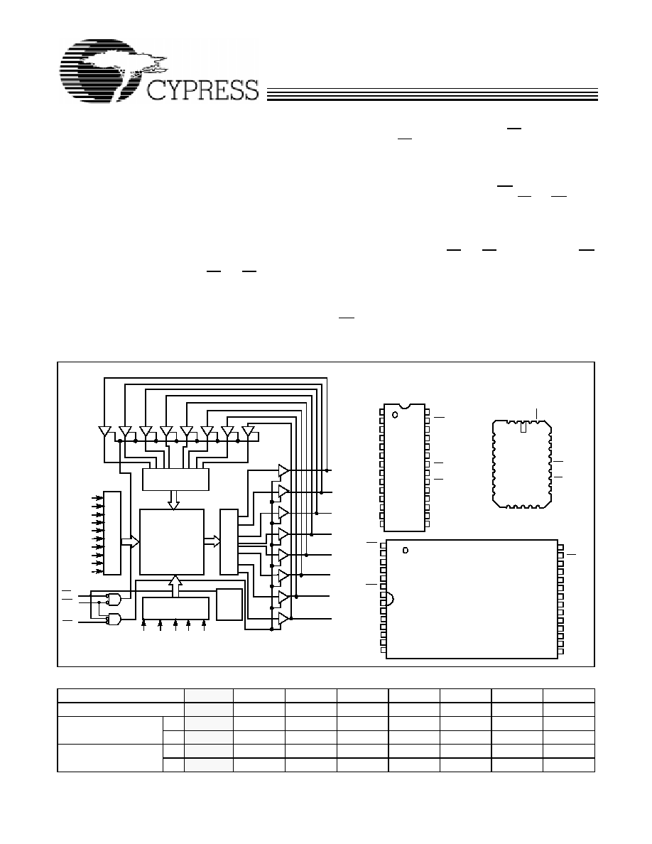
The CY7C199 is a high-performance CMOS static RAM orga-
nized as 32,768 words by 8 bits. Easy memory expansion is
provided by an active LOW chip enable (CE) and active LOW
output enable (OE) and three-state drivers. This device has an
automatic power-down feature, reducing the power consump-
tion by 81% when deselected. The CY7C199 is in the standard
300-mil-wide DIP, SOJ, and LCC packages.
An active LOW write enable signal (WE) controls the writ-
ing/reading operation of the memory. When CE and WE inputs
are both LOW, data on the eight data input/output pins (I/O
0
through I/O
7
) is written into the memory location addressed by
the address present on the address pins (A
0
through A
14
).
Reading the device is accomplished by selecting the device
and enabling the outputs, CE and OE active LOW, while WE
remains inactive or HIGH. Under these conditions, the con-
tents of the location addressed by the information on address
pins are present on the eight data input/output pins.
The input/output pins remain in a high-impedance state unless
the chip is selected, outputs are enabled, and write enable
(WE) is HIGH. A die coat is used to improve alpha immunity.
Logic Block Diagram
Pin Configurations
A
1
A
2
A
3
A
4
A
5
A
6
A
7
A
8
COLUMN
DECODER
RO
W
DE
CO
DE
R
SEN
S
E
AM
PS
INPUT BUFFER
POWER
DOWN
WE
OE
I/O
0
CE
I/O
1
I/O
2
I/O
3
1
2
3
4
5
6
7
8
9
10
11
14
15
16
20
19
18
17
21
24
23
22
Top View
DIP / SOJ / SOIC
12
13
25
28
27
26
GND
A
6
A
7
A
8
A
9
A
10
A
11
A
12
A
13
WE
V
CC
A
4
A
3
A
2
A
1
I/O
7
I/O
6
I/O
5
I/O
4
A
14
A
5
I/O
0
I/O
1
I/O
2
CE
OE
A
0
I/O
3
1024 x 32 x 8
ARRAY
I/O
7
I/O
6
I/O
5
I/O
4
A
9
A
0
A
11
A
13
A
12
A
14
A
10
28
4
5
6
7
8
9
10
3 2 1
27
1314151617
26
25
24
23
22
21
20
11
12
19
18
A
7
V
CC
I/O
5
GN
D
WE
A
6
A
5
I/O
4
I/O
3
I/O
2
A
8
A
9
A
10
A
11
A
12
A
13
A
14
CE
A
3
A
2
A
1
A
0
I/O
1
I/O
7
I/O
6
A
4
OE
I/O
0
Top View
LCC
C1991
C1992
C1993
22
23
24
25
26
27
28
1
2
5
10
11
15
14
13
12
16
19
18
17
3
4
20
21
7
6
8
9
OE
A
1
A
2
A
3
A
4
WE
V
CC
A
5
A
6
A
7
A
8
A
9
A
0
CE
I/O
7
I/O
6
I/O
5
GND
I/O
2
I/O
1
I/O
4
I/O
0
A
14
A
10
A
11
A
13
A
12
C1994
I/O
3
TSOP I
Top View
(not to scale)
Selection Guide
7C199-8
7C199-10
7C199-12
7C199-15
7C199-20
7C199-25
7C199-35
7C199-45
Maximum Access Time (ns)
8
10
12
15
20
25
35
45
Maximum Operating
Current (mA)
120
110
160
155
150
150
140
140
L
90
90
90
90
80
70
Maximum CMOS
Standby Current (mA)
0.5
0.5
10
10
10
10
10
10
L
0.05
0.05
0.05
0.05
0.05
0.05
Shaded area contains preliminary information.
CY7C199
2
Maximum Ratings
(Above which the useful life may be impaired. For user guide-
lines, not tested.)
Storage Temperature ................................. 65
°
C to +150
°
C
Ambient Temperature with
Power Applied ............................................. 55
°
C to +125
°
C
Supply Voltage to Ground Potential
(Pin 28 to Pin 14) ........................................... 0.5V to +7.0V
DC Voltage Applied to Outputs
in High Z State
[1]
....................................0.5V to V
CC
+ 0.5V
DC Input Voltage
[1]
.................................0.5V to V
CC
+ 0.5V
Output Current into Outputs (LOW)............................. 20 mA
Static Discharge Voltage .......................................... >2001V
(per MIL-STD-883, Method 3015)
Latch-Up Current .................................................... >200 mA
Operating Range
Range
Ambient Temperature
[2]
V
CC
Commercial
0
°
C to +70
°
C
5V
±
10%
Industrial
40
°
C to +85
°
C
5V
±
10%
Military
55
°
C to +125
°
C
5V
±
10%
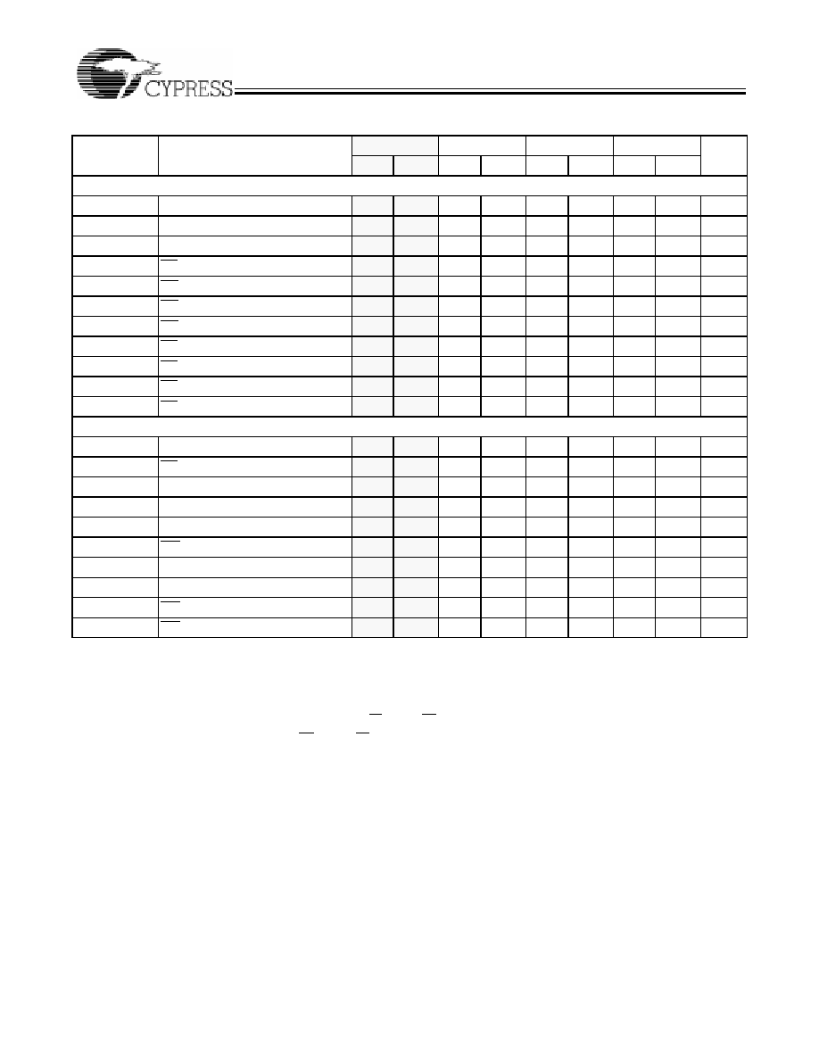
Electrical Characteristics
Over the Operating Range
[3]
7C199-8
7C199-10
7C199-12
7C199-15
Parameter
Description
Test Conditions
Min.
Max.
Min.
Max.
Min.
Max.
Min.
Max.
Unit
V
OH
Output HIGH
Voltage
V
CC
=Min., I
OH
=4.0 mA
2.4
2.4
2.4
2.4
V
V
OL
Output LOW
Voltage
V
CC
=Min., I
OL
=8.0 mA
0.4
0.4
0.4
0.4
V
V
IH
Input HIGH
Voltage
2.2
V
CC
+0.3V
2.2
V
CC
+0.3V
2.2
V
CC
+0.3V
2.2
V
CC
+0.3V
V
V
IL
Input LOW
Voltage
0.5
0.8
0.5
0.8
0.5
0.8
0.5
0.8
V
I
IX
Input Load
Current
GND < V
I
< V
CC
5
+5
5
+5
5
+5
5
+5
µ
A
I
OZ
Output Leakage
Current
GND < V
O
< V
CC
,
Output Disabled
5
+5
5
+5
5
+5
5
+5
µ
A
I
CC
V
CC
Operating
Supply Current
V
CC
= Max.,
I
OUT
= 0 mA,
f = f
MAX
= 1/t
RC
Com'l
120
110
160
155
mA
L
85
85
100
mA
Mil
180
mA
I
SB1
Automatic CE
Power-Down
Current-- TTL
Inputs
Max. V
CC
, CE >
V
IH
,
V
IN
> V
IH
or
V
IN
< V
IL
, f = f
MAX
Com'l
5
5
30
30
mA
L
5
5
5
mA
I
SB2
Automatic CE
Power-Down
Current-- CMOS
Inputs
Max. V
CC
,
CE > V
CC
0.3V
V
IN
> V
CC
0.3V
or V
IN
< 0.3V, f = 0
Com'l
0.5
0.5
10
10
mA
L
0.05
0.05
0.05
0.05
mA
Mil
15
mA
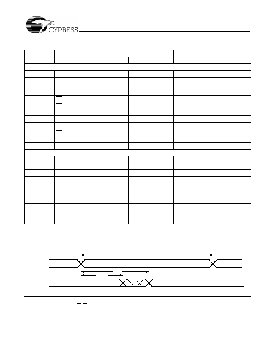
Shaded area contains preliminary information.
Notes:
1.
V
IL
(min.)
= 2.0V for pulse durations of less than 20 ns.
2.
T
A
is the "instant on" case temperature.
3.
See the last page of this specification for Group A subgroup testing information.
CY7C199
3
]
Electrical Characteristics
Over the Operating Range
[3]
(continued)
7C199-20
7C199-25
7C199-35
7C199-45
Parameter
Description
Test Conditions
Min.
Max.
Min.
Max.
Min.
Max.
Min.
Max.
Unit
V
OH
Output HIGH
Voltage
V
CC
=Min., I
OH
=4.0 mA
2.4
2.4
2.4
2.4
V
V
OL
Output LOW
Voltage
V
CC
=Min., I
OL
=8.0 mA
0.4
0.4
0.4
0.4
V
V
IH
Input HIGH
Voltage
2.2
V
CC
+0.3V
2.2
V
CC
+0.3V
2.2
V
CC
+0.3V
2.2
V
CC
+0.3V
V
V
IL
Input LOW
Voltage
0.5
0.8
-0.5
0.8
-0.5
0.8
-0.5
0.8
V
I
IX
Input Load
Current
GND < V
I
< V
CC
5
+5
5
+5
5
+5
5
+5
µ
A
I
OZ
Output Leakage
Current
GND < V
I
< V
CC
,
Output Disabled
5
+5
5
+5
5
+5
5
+5
µ
A
I
CC
V
CC
Operating
Supply Current
V
CC
= Max.,
I
OUT
= 0 mA,
f = f
MAX
= 1/t
RC
Com'l
150
150
140
140
mA
L
90
80
70
70
mA
Mil
170
150
150
150
mA
I
SB1
Automatic CE
Power-Down
Current--
TTL Inputs
Max. V
CC
, CE > V
IH
,
V
IN
> V
IH
or V
IN
< V
IL
, f = f
MAX
Com'l
30
30
25
25
mA
L
5
5
5
5
mA
I
SB2
Automatic CE
Power-Down
Current--
CMOS Inputs
Max. V
CC
,
CE > V
CC
0.3V
V
IN
> V
CC
0.3V or
V
IN
< 0.3V, f=0
Com'l
10
10
10
10
mA
L
0.05
0.05
0.05
0.05
µ
A
Mil
15
15
15
15
mA
Capacitance
[4]
Parameter
Description
Test Conditions
Max.
Unit
C
IN
Input Capacitance
T
A
= 25
°
C, f = 1 MHz,
V
CC
= 5.0V
8
pF
C
OUT
Output Capacitance
8
pF
CY7C199
4
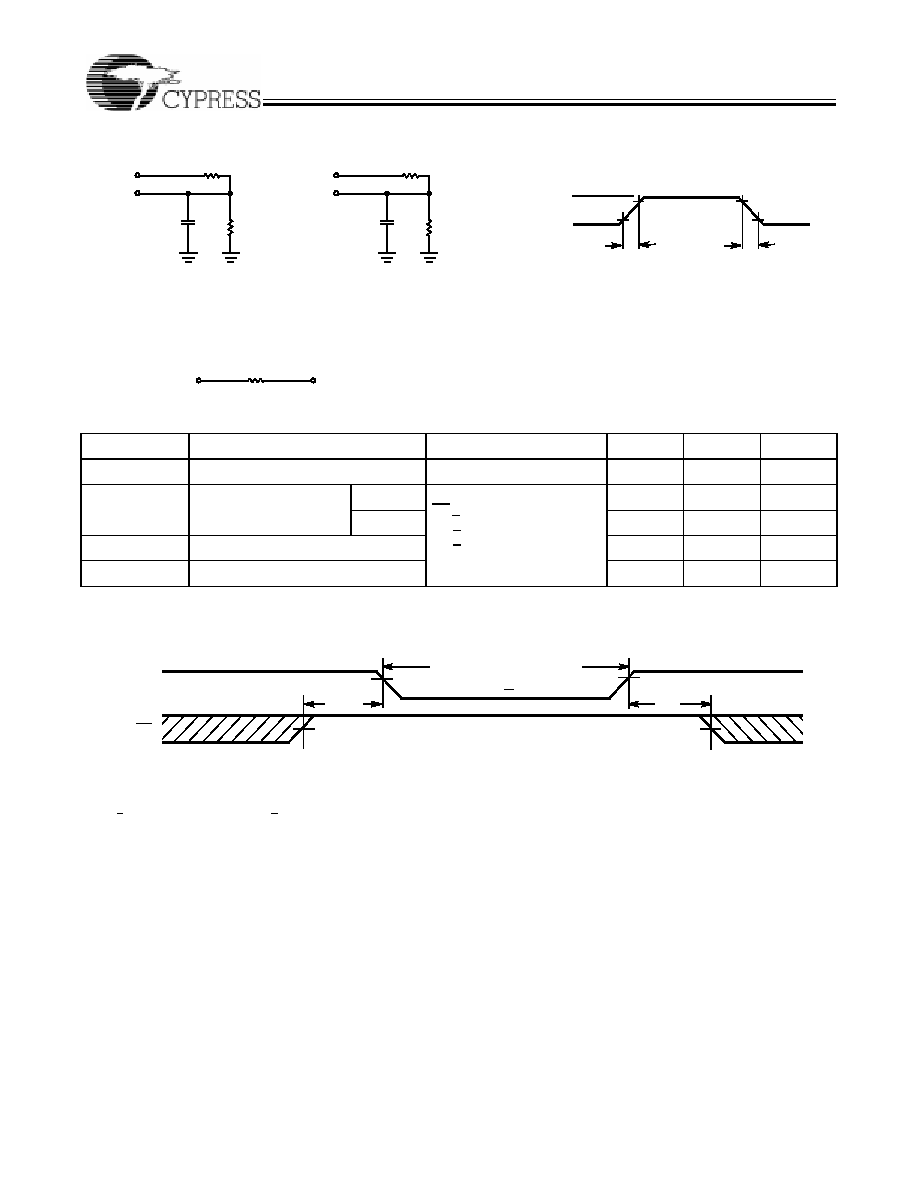
AC Test Loads and Waveforms
[5]
Data Retention Characteristics
Over the Operating Range (L version only)
Parameter
Description
Conditions
[6]
Min.
Max.
Unit
V
DR
V
CC
for Data Retention
2.0
V
I
CCDR
Data Retention Current
Com'l
V
CC
= V
DR
= 2.0V,
CE > V
CC
0.3V,
V
IN
> V
CC
0.3V or
V
IN
< 0.3V
µ
A
Com'l L
10
µ
A
t
CDR
[4]
Chip Deselect to Data Retention Time
0
ns
t
R
[5]
Operation Recovery Time
t
RC
ns
3.0V
5V
OUTPUT
R1 481
R2
255
30 pF
INCLUDING
JIGAND
SCOPE
GND
90%
10%
90%
10%
t
r
t
r
5V
OUTPUT
R1 481
R2
255
5 pF
INCLUDING
JIGAND
SCOPE
(a)
(b)
OUTPUT
1.73V
Equivalent to:
THÉ VENIN EQUIVALENT
ALL INPUT PULSES
C1995
C1996
167
Data Retention Waveform
Notes:
4.
Tested initially and after any design or process changes that may affect these parameters.
5.
t
R
< 3 ns for the -12 and -15 speeds. t
R
< 5 ns for the -20 and slower speeds.
6.
No input may exceed V
CC
+ 0.5V.
C1997
3.0V
3.0V
t
CDR
V
DR
> 2V
DATA RETENTION MODE
t
R
CE
V
CC
CY7C199
5
Switching Characteristics
Over the Operating Range
[3, 7]
7C199-8
7C199-10
7C199-12
7C199-15
Unit
Parameter
Description
Min.
Max.
Min.
Max.
Min.
Max.
Min.
Max.
READ CYCLE
t
RC
Read Cycle Time
8
10
12
15
ns
t
AA
Address to Data Valid
8
10
12
15
ns
t
OHA
Data Hold from Address Change
3
3
3
3
ns
t
ACE
CE LOW to Data Valid
8
10
12
15
ns
t
DOE
OE LOW to Data Valid
4.5
5
5
7
ns
t
LZOE
OE LOW to Low Z
[8]
0
0
0
0
ns
t
HZOE
OE HIGH to High Z
[8, 9]
5
5
5
7
ns
t
LZCE
CE LOW to Low Z
[8]
3
3
3
3
ns
t
HZCE
CE HIGH to High Z
[8,9]
4
5
5
7
ns
t
PU
CE LOW to Power-Up
0
0
0
0
ns
t
PD
CE HIGH to Power-Down
8
10
12
15
ns
WRITE CYCLE
[10, 11]
t
WC
Write Cycle Time
8
10
12
15
ns
t
SCE
CE LOW to Write End
7
7
9
10
ns
t
AW
Address Set-Up to Write End
7
7
9
10
ns
t
HA
Address Hold from Write End
0
0
0
0
ns
t
SA
Address Set-Up to Write Start
0
0
0
0
ns
t
PWE
WE Pulse Width
7
7
8
9
ns
t
SD
Data Set-Up to Write End
5
5
8
9
ns
t
HD
Data Hold from Write End
0
0
0
0
ns
t
HZWE
WE LOW to High Z
[9]
5
6
7
7
ns
t
LZWE
WE HIGH to Low Z
[8]
3
3
3
3
ns
Shaded area contains preliminary information.
Notes:
7.
Test conditions assume signal transition time of 3 ns or less for -12 and -15 speeds and 5 ns or less for -20 and slower speeds, timing reference levels of 1.5V,
input pulse levels of 0 to 3.0V, and output loading of the specified I
OL
/I
OH
and 30-pF load capacitance.
8.
At any given temperature and voltage condition, t
HZCE
is less than t
LZCE
, t
HZOE
is less than t
LZOE
, and t
HZWE
is less than t
LZWE
for any given device.
9.
t
HZOE
, t
HZCE
, and t
HZWE
are specified with C
L
= 5 pF as in part (b) of AC Test Loads. Transition is measured
±
500 mV from steady-state voltage.
10. The internal write time of the memory is defined by the overlap of CE LOW and WE LOW. Both signals must be LOW to initiate a write and either signal can terminate
a write by going HIGH. The data input set-up and hold timing should be referenced to the rising edge of the signal that terminates the write.
11. The minimum write cycle time for write cycle #3 (WE controlled, OE LOW) is the sum of t
HZWE
and t
SD
.
CY7C199
6
Switching Characteristics
Over the Operating Range
[3,7]
(continued)
7C199-20
7C199-25
7C199-35
7C199-45
Parameter
Description
Min.
Max.
Min.
Max.
Min.
Max.
Min.
Max.
Unit
READ CYCLE
t
RC
Read Cycle Time
20
25
35
45
ns
t
AA
Address to Data Valid
20
25
35
45
ns
t
OHA
Data Hold from Address
Change
3
3
3
3
ns
t
ACE
CE LOW to Data Valid
20
25
35
45
ns
t
DOE
OE LOW to Data Valid
9
10
16
16
ns
t
LZOE
OE LOW to Low Z
[8]
0
0
0
0
ns
t
HZOE
OE HIGH to High Z
[8,9]
9
11
15
15
ns
t
LZCE
CE LOW to Low Z
[8]
3
3
3
3
ns
t
HZCE
CE HIGH to High Z
[8,9]
9
11
15
15
ns
t
PU
CE LOW to Power-Up
0
0
0
0
ns
t
PD
CE HIGH to Power-Down
20
20
20
25
ns
WRITE CYCLE
[10,11]
t
WC
Write Cycle Time
20
25
35
45
ns
t
SCE
CE LOW to Write End
15
18
22
22
ns
t
AW
Address Set-Up to Write End
15
20
30
40
ns
t
HA
Address Hold from Write End
0
0
0
0
ns
t
SA
Address Set-Up to Write Start
0
0
0
0
ns
t
PWE
WE Pulse Width
15
18
22
22
ns
t
SD
Data Set-Up to Write End
10
10
15
15
ns
t
HD
Data Hold from Write End
0
0
0
0
ns
t
HZWE
WE LOW to High Z
[9]
10
11
15
15
ns
t
LZWE
WE HIGH to Low Z
[8]
3
3
3
3
ns
Switching Waveforms
Read Cycle No. 1
[12, 13]
Notes:
12. Device is continuously selected. OE, CE = V
IL
.
13. WE is HIGH for read cycle.
ADDRESS
DATA OUT
PREVIOUS DATA VALID
DATA VALID
t
RC
t
AA
t
OHA
C1998
CY7C199
7
Read Cycle No. 2
[13, 14]
Write Cycle No. 1 (WE Controlled)
[10, 15, 16]
Write Cycle No. 2 (CE Controlled)
[10, 15, 16]
Notes:
14. Address valid prior to or coincident with CE transition LOW.
15. Data I/O is high impedance if OE = V
IH
.
16. If CE goes HIGH simultaneously with WE HIGH, the output remains in a high-impedance state.
Switching Waveforms
(continued)
50%
50%
DATA VALID
t
RC
t
ACE
t
DOE
t
LZOE
t
LZCE
t
PU
DATA OUT
HIGH IMPEDANCE
IMPEDANCE
ICC
ISB
t
HZOE
t
HZCE
t
PD
OE
CE
HIGH
V
CC
SUPPLY
CURRENT
C1999
t
HD
t
SD
t
PWE
t
SA
t
HA
t
AW
t
WC
DATA I/O
ADDRESS
CE
WE
OE
t
HZOE
C19910
DATA
IN
VALID
t
WC
t
AW
t
SA
t
HA
t
HD
t
SD
t
SCE
WE
DATA I/O
ADDRESS
CE
C19911
DATA
IN
VALID
CY7C199
8
Write Cycle No. 3 (WE Controlled OE LOW)
[11, 16]
Switching Waveforms
(continued)
DATA I/O
ADDRESS
t
HD
t
SD
t
LZWE
t
SA
t
HA
t
AW
t
WC
CE
WE
t
HZWE
C19912
DATA
IN
VALID
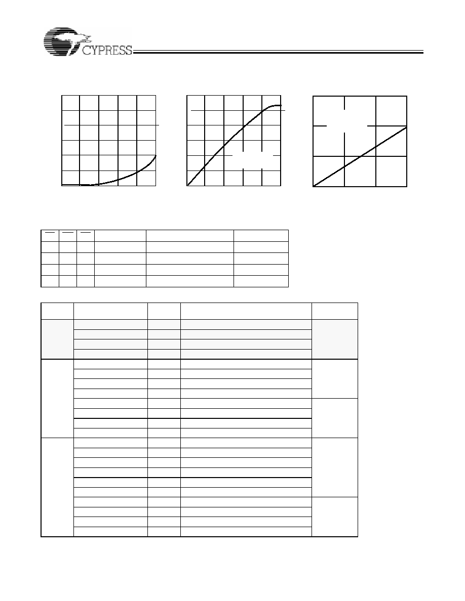
Typical DC and AC Characteristics
1.2
1.4
1.0
0.6
0.4
0.2
4.0
4.5
5.0
5.5
6.0
1.6
1.4
1.2
1.0
0.8
55
25
125
55
25
125
1.2
1.0
0.8
NORM
AL
I
Z
E
D t
AA
120
100
80
60
40
20
0.0
1.0
2.0
3.0
4.0
OUT
P
UT
SOURCE CUR
RENT
(
m
A
)
SUPPLY VOLTAGE (V)
NORMALIZED SUPPLY CURRENT
vs. SUPPLY VOLTAGE
NORMALIZED ACCESS TIME
vs. AMBIENT TEMPERATURE
AMBIENT TEMPERATURE (
°
C)
NORMALIZED SUPPLY CURRENT
vs. AMBIENT TEMPERATURE
AMBIENT TEMPERATURE (
°
C)
OUTPUT VOLTAGE (V)
OUTPUT SOURCE CURRENT
vs. OUTPUT VOLTAGE
0.0
0.8
1.4
1.1
1.0
0.9
4.0
4.5
5.0
5.5
6.0
NORM
AL
I
Z
E
D t
SUPPLY VOLTAGE (V)
NORMALIZED ACCESS TIME
vs. SUPPLY VOLTAGE
120
140
100
60
40
20
0.0
1.0
2.0
3.0
4.0
OUT
P
UT
S
I
NK CURRENT
(m
A
)
0
80
OUTPUT VOLTAGE (V)
OUTPUT SINK CURRENT
vs. OUTPUT VOLTAGE
0.6
0.4
0.2
0.0
NO
RM
AL
IZ
ED I
CC
,I
SB
NORM
A
L
I
Z
ED I
CC
,I
SB
I
SB
I
CC
I
CC
V
CC
=5.0V
V
CC
=5.0V
T
A
=25
°
C
V
CC
=5.0V
T
A
=25
°
C
I
SB
T
A
=25
°
C
0.6
0.8
0
AA
1.3
1.2
V
IN
=5.0V
T
A
=25
°
C
1.4
V
CC
=5.0V
V
IN
=5.0V
CY7C199
9
Typical DC and AC Characteristics
(continued)
3.0
2.5
2.0
1.5
1.0
0.5
0.0
1.0
2.0
3.0
4.0
NO
RM
AL
I
Z
ED I
PO
SUPPLY VOLTAGE (V)
TYPICAL POWER-ON CURRENT
vs. SUPPLY VOLTAGE
30.0
25.0
20.0
15.0
10.0
5.0
0
200
400
600
800
D
E
L
T
A
t
(n
s
)
AA
CAPACITANCE (pF)
TYPICAL ACCESS TIME CHANGE
vs. OUTPUT LOADING
1.25
1.00
0.75
10
20
30
40
NO
RM
AL
I
Z
ED I
CC
CYCLE FREQUENCY (MHz)
NORMALIZED I
CC
vs. CYCLE TIME
0.0
5.0
0.0
1000
0.50
V
CC
=4.5V
T
A
=25
°
C
V
CC
=5.0V
T
A
=25
°
C
V
IN
=0.5V
Truth Table
CE
WE
OE Inputs/Outputs
Mode
Power
H
X
X
High Z
Deselect/Power-Down
Standby (I
SB
)
L
H
L
Data Out
Read
Active (I
CC
)
L
L
X
Data In
Write
Active (I
CC
)
L
H
H
High Z
Deselect, Output Disabled
Active (I
CC
)
Ordering Information
Speed
(ns)
Ordering Code
Package
Name
Package Type
Operating
Range
8
CY7C199-8VC
V21
28-Lead Molded SOJ
Commercial
CY7C199-8ZC
Z28
28-Lead Thin Small Outline Package
CY7C199L-8VC
V21
28-Lead Molded SOJ
CY7C199L-8ZC
Z28
28-Lead Thin Small Outline Package
10
CY7C199-10VC
V21
28-Lead Molded SOJ
Commercial
CY7C199-10ZC
Z28
28-Lead Thin Small Outline Package
CY7C199L-10VC
V21
28-Lead Molded SOJ
CY7C199L-10ZC
Z28
28-Lead Thin Small Outline Package
CY7C199-10VI
V21
28-Lead Molded SOJ
Industrial
CY7C199-10ZI
Z28
28-Lead Thin Small Outline Package
CY7C199L-10VI
V21
28-Lead Molded SOJ
CY7C199L-10ZI
Z28
28-Lead Thin Small Outline Package
12
CY7C199-12PC
P21
28-Lead (300-Mil) Molded DIP
Commercial
CY7C199-12VC
V21
28-Lead Molded SOJ
CY7C199-12ZC
Z28
28-Lead Thin Small Outline Package
CY7C199L-12PC
P21
28-Lead (300-Mil) Molded DIP
CY7C199L-12VC
V21
28-Lead Molded SOJ
CY7C199L-12ZC
Z28
28-Lead Thin Small Outline Package
CY7C199-12VI
V21
28-Lead Molded SOJ
Industrial
CY7C199-12ZI
Z28
28-Lead Thin Small Outline Package
CY7C199L-12VI
V21
28-Lead Molded SOJ
CY7C199L-12ZI
Z28
28-Lead Thin Small Outline Package
Shaded area contains preliminary information. Contact your Cypress sales representative for availability
CY7C199
10
15
CY7C199-15PC
P21
28-Lead (300-Mil) Molded DIP
Commercial
CY7C199-15VC
V21
28-Lead Molded SOJ
CY7C199-15ZC
Z28
28-Lead Thin Small Outline Package
CY7C199L-15PC
P21
28-Lead (300-Mil) Molded DIP
CY7C199L-15VC
V21
28-Lead Molded SOJ
CY7C199L-15ZC
Z28
28-Lead Thin Small Outline Package
CY7C199-15VI
V21
28-Lead Molded SOJ
Industrial
CY7C199-15ZI
Z28
28-Lead Thin Small Outline Package
CY7C199-15DMB
D22
28-Lead (300-Mil) CerDIP
Military
CY7C199-15LMB
L54
28-Pin Rectangular Leadless Chip Carrier
CY7C199L-15DMB
D22
28-Lead (300-Mil) CerDIP
CY7C199L-15LMB
L54
28-Pin Rectangular Leadless Chip Carrier
20
CY7C199-20PC
P21
28-Lead (300-Mil) Molded DIP
Commercial
CY7C199-20VC
V21
28-Lead Molded SOJ
CY7C199-20ZC
Z28
28-Lead Thin Small Outline Package
CY7C199L-20PC
P21
28-Lead (300-Mil) Molded DIP
CY7C199L-20VC
V21
28-Lead Molded SOJ
CY7C199L-20ZC
Z28
28-Lead Thin Small Outline Package
CY7C199-20VI
V21
28-Lead Molded SOJ
Industrial
CY7C199-20ZI
Z28
28-Lead Thin Small Outline Package
CY7C199-20DMB
D22
28-Lead (300-Mil) CerDIP
Military
CY7C199-20LMB
L54
28-Pin Rectangular Leadless Chip Carrier
CY7C199L-20DMB
D22
28-Lead (300-Mil) CerDIP
CY7C199L-20LMB
L54
28-Pin Rectangular Leadless Chip Carrier
25
CY7C199-25PC
P21
28-Lead (300-Mil) Molded DIP
Commercial
CY7C199-25SC
S21
28-Lead Molded SOIC
CY7C199-25VC
V21
28-Lead Molded SOJ
CY7C199-25ZC
Z28
28-Lead Thin Small Outline Package
CY7C199L-25ZI
Z28
28-Lead Thin Small Outline Package
Industrial
CY7C199-25DMB
D22
28-Lead (300-Mil) CerDIP
Military
CY7C199-25LMB
L54
28-Pin Rectangular Leadless Chip Carrier
35
CY7C199-35PC
P21
28-Lead (300-Mil) Molded DIP
Commercial
CY7C199-35SC
S21
28-Lead Molded SOIC
CY7C199-35VC
V21
28-Lead Molded SOJ
CY7C199-35ZC
Z28
28-Lead Thin Small Outline Package
CY7C199-35DMB
D22
28-Lead (300-Mil) CerDIP
Military
CY7C199-35LMB
L54
28-Pin Rectangular Leadless Chip Carrier
45
CY7C199-45DMB
D22
28-Lead (300-Mil) CerDIP
Military
CY7C199-45LMB
L54
28-Pin Rectangular Leadless Chip Carrier
Ordering Information
(continued)
Speed
(ns)
Ordering Code
Package
Name
Package Type
Operating
Range
Shaded area contains preliminary information. Contact your Cypress sales representative for availability
CY7C199
11
MILITARY SPECIFICATIONS
Group A Subgroup Testing
DC Characteristics
Parameter
Subgroups
V
OH
1, 2, 3
V
OL
1, 2, 3
V
IH
1, 2, 3
V
IL
Max.
1, 2, 3
I
IX
1, 2, 3
I
OZ
1, 2, 3
I
CC
1, 2, 3
I
SB1
1, 2, 3
I
SB2
1, 2, 3
Switching Characteristics
Parameter
Subgroups
READ CYCLE
t
RC
7, 8, 9, 10, 11
t
AA
7, 8, 9, 10, 11
t
OHA
7, 8, 9, 10, 11
t
ACE
7, 8, 9, 10, 11
t
DOE
7, 8, 9, 10, 11
WRITE CYCLE
t
WC
7, 8, 9, 10, 11
t
AA
7, 8, 9, 10, 11
t
AW
7, 8, 9, 10, 11
t
HA
7, 8, 9, 10, 11
t
SA
7, 8, 9, 10, 11
t
PWE
7, 8, 9, 10, 11
t
SD
7, 8, 9, 10, 11
t
HD
7, 8, 9, 10, 11
Document #: 3800239E
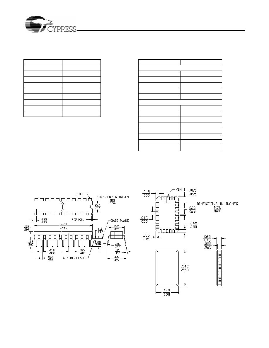
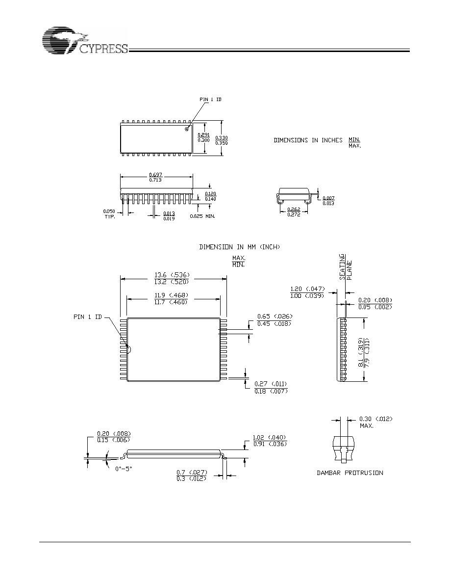
Package Diagrams
28-Lead (300-Mil) CerDIP D22
MILSTD1835
D15 Config.A
28-Pin Rectangular Leadless Chip Carrier L54
MILSTD1835 C11A
CY7C199
12
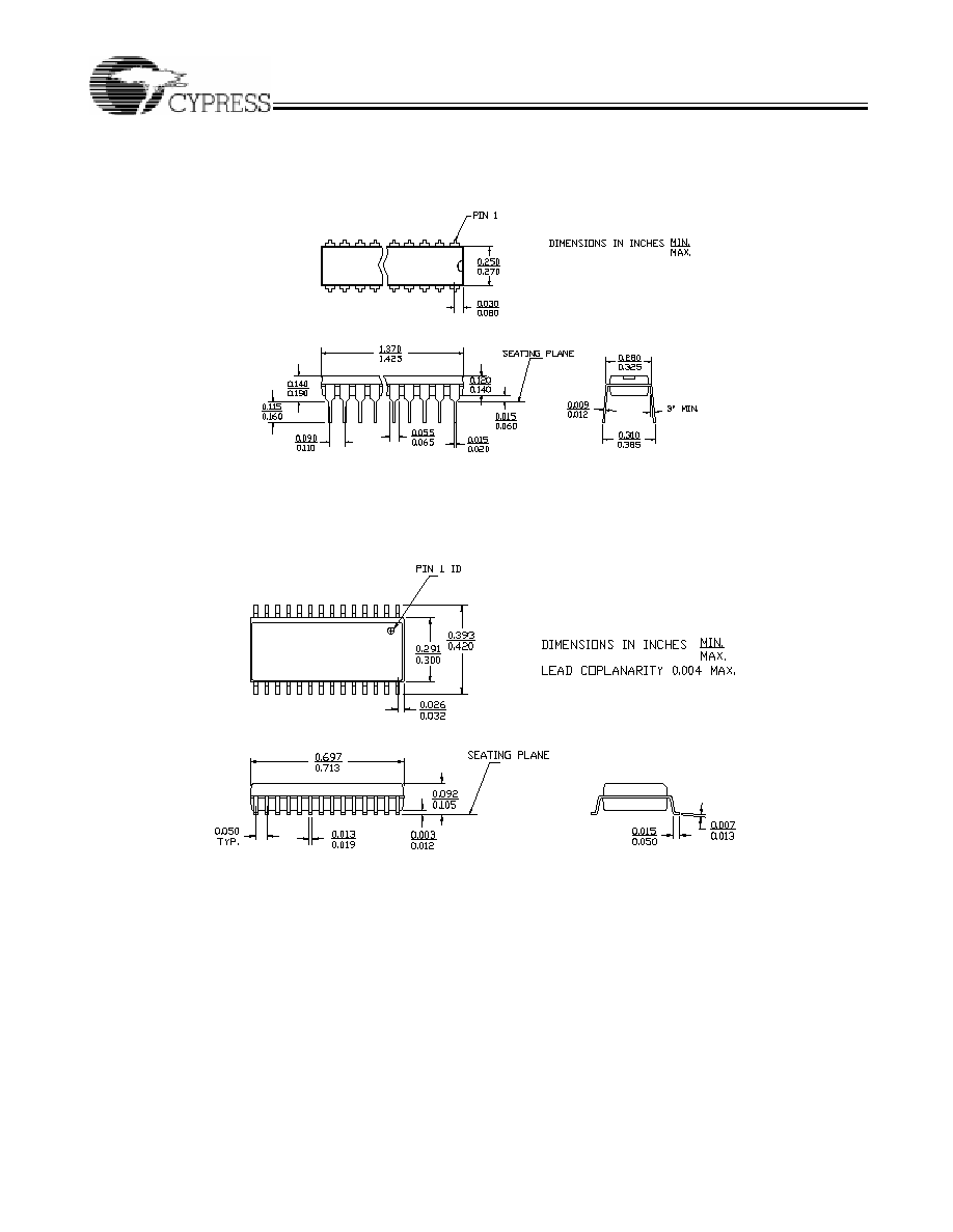
Package Diagrams
(continued)
28-Lead (300-Mil) Molded DIP P21
28-Lead (300-Mil) Molded SOIC S21
CY7C199
© Cypress Semiconductor Corporation, 1998. The information contained herein is subject to change without notice. Cypress Semiconductor Corporation assumes no responsibility for the use
of any circuitry other than circuitry embodied in a Cypress Semiconductor product. Nor does it convey or imply any license under patent or other rights. Cypress Semiconductor does not authorize
its products for use as critical components in life-support systems where a malfunction or failure may reasonably be expected to result in significant injury to the user. The inclusion of Cypress
Semiconductor products in life-support systems application implies that the manufacturer assumes all risk of such use and in doing so indemnifies Cypress Semiconductor against all charges.
Package Diagrams
(continued)
28-Lead (300-Mil) Molded SOJ V21
28-Lead Thin Small Outline Package Z28