Untitled Document
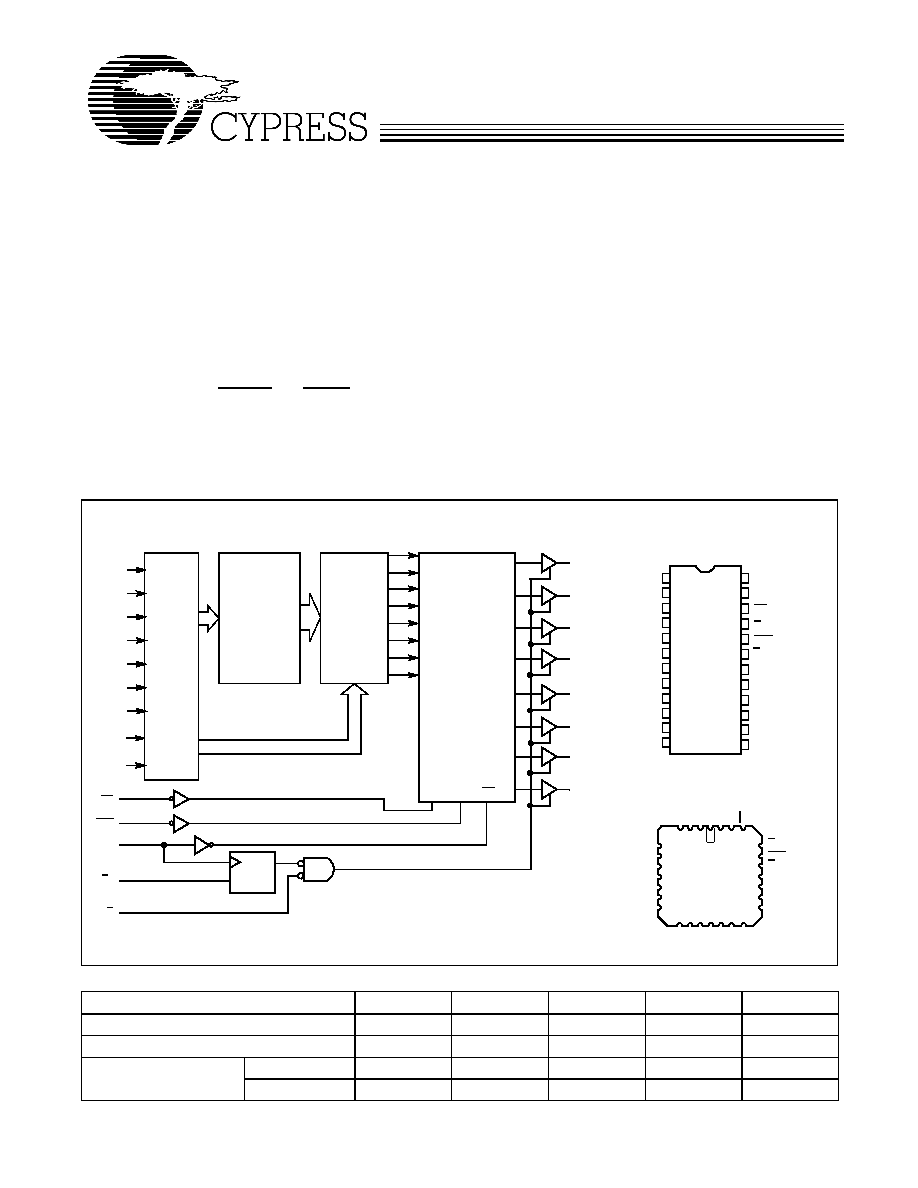
512 x 8 Registered PROM
CY7C225A
Cypress Semiconductor Corporation
·
3901 North First Street
·
San Jose
·
CA 95134
·
408-943-2600
Document #: 38-04001 Rev. **
Revised March 4, 2002
25A
Features
· CMOS for optimum speed/power
· High speed
-- 18 ns address set-up
-- 12 ns clock to output
· Low power
-- 495 mW (commercial)
-- 660 mW (military)
· Synchronous and asynchronous output enables
· On-chip edge-triggered registers
· Buffered common PRESET and CLEAR inputs
· EPROM technology, 100% programmable
· Slim 300-mil, 24-pin plastic or hermetic DIP, 28-pin LCC,
or 28-pin PLCC
· 5V
±
10% V
CC
, commercial and military
· TTL-compatible I/O
· Direct replacement for bipolar PROMs
· Capable of withstanding greater than 2001V static
discharge
Functional Description
The CY7C225A is a high-performance 512 word by 8 bit elec-
trically programmable read only memory packaged in a slim
300-mil plastic or hermetic DIP, 28-pin leadless chip carrier,
and 28-pin PLCC. The memory cells utilize proven EPROM
floating gate technology and byte-wide intelligent program-
ming algorithms.
The CY7C225A replaces bipolar devices and offers the advan-
tages of lower power, superior performance, and high pro-
gramming yield. The EPROM cell requires only 12.5V for the
supervoltage and low current requirements allow for gang pro-
gramming. The EPROM cells allow for each memory location
to be tested 100%, as each location is written into, erased, and
repeatedly exercised prior to encapsulation. Each PROM is
also tested for AC performance to guarantee that after custom-
er programming the product will meet AC specification limits.
Logic Block Diagram
Pin Configurations
1
2
3
4
5
6
7
8
9
10
11
12
16
17
18
19
20
24
23
22
21
13
14
A
7
A
6
A
5
A
4
A
3
A
2
A
1
A
0
O
0
O
1
O
2
GND
V
CC
A
8
PS
E
CLR
CP
O
7
O
6
O
4
O
5
O
3
PROGRAMMABLE
ARRAY
MULTIPLEXER
15
8-BIT
EDGE-
REGISTER
TRIGGERED
O
7
O
6
O
5
O
4
O
3
O
2
O
1
O
0
PS
CLR
S
R
CP
CP
E
S
E
E
S
28
4
5
6
7
8
9
10
3 2 1
27
13
26
25
24
23
22
21
20
11
12
19
A
5
V
CC
GND
A
6
A
7
O
3
O
1
O
0
18
O
4
O
5
NC
A
0
A
4
A
3
E
NC
NC
NC
CLR
E
S
O
7
O
6
A
2
A
1
CP
O
2
A
8
PS
DIP
LCC/PLCC
Top View
Top View
ADDRESS
DECODER
A
0
A
1
A
2
A
3
A
4
A
5
A
6
A
8
A
7
COLUMN
ADDRESS
ROW
ADDRESS
141516 17
Selection Guide
7C225A-18
7C225A-25
7C225A-30
7C225A-35
7C225A-40
Minimum Address Set-Up Time (ns)
18
25
30
35
40
Maximum Clock to Output (ns)
12
12
15
20
25
Maximum Operating
Current (mA)
Commercial
90
90
90
90
Military
120
120
120
120
CY7C225A
Document #: 38-04001 Rev. **
Page 2 of 10
Maximum Ratings
(Above which the useful life may be impaired. For user guide-
lines, not tested.)
Storage Temperature
..................................... -
65
°
C to +150
°
C
Ambient Temperature with
Power Applied
.................................................. -
55
°
C to +125
°
C
Supply Voltage to Ground Potential
(Pin 24 to Pin 12)
.................................................-
0.5V to +7.0V
DC Voltage Applied to Outputs
in High Z State
.....................................................-
0.5V to +7.0V
DC Input Voltage
.................................................-
3.0V to +7.0V
DC Program Voltage (Pins 7, 18, 20)............................13.0V
Static Discharge Voltage ........................................... >2001V
(per MIL-STD-883, Method 3015)
Latch-Up Current ..................................................... >200 mA
Operating Range
Range
Ambient
Temperature
V
CC
Commercial
0
°
C to +70
°
C
5V ± 10%
Industrial
[1]
-
40
°
C to +85
°
C
5V ± 10%
Military
[2]
-
55
°
C to +125
°
C
5V ± 10%
Electrical Characteristics
Over the Operating Range
[3,4]
Parameter
Description
Test Conditions
Min.
Max.
Unit
V
OH
Output HIGH Voltage
V
CC
= Min., I
OH
=
-
4.0 mA
V
IN
= V
IH
or V
IL
2.4
V
V
OL
Output LOW Voltage
V
CC
= Min., I
OL
= 16 mA
V
IN
= V
IH
or V
IL
0.4
V
V
IH
Input HIGH
Level
Guaranteed Input Logical HIGH Voltage for
All Inputs
2.0
V
V
IL
Input LOW Level
Guaranteed Input Logical LOW Voltage for All
Inputs
0.8
V
I
IX
Input Leakage Current
GND < V
IN
< V
CC
-
10
+10
µ
A
V
CD
Input Clamp Diode Voltage
Note 4
I
OZ
Output Leakage Current
GND < V
OUT
< V
CC
, Output Disabled
[5]
-
10
+10
µ
A
I
OS
Output Short Circuit Current
V
CC
= Max., V
OUT
= 0.0V
[6]
-
20
-
90
mA
I
CC
Power Supply Current
I
OUT
= 0 mA
V
CC
= Max.
Commercial
90
mA
Military
120
V
PP
Programming Supply Voltage
12
13
V
I
PP
Programming Supply Current
50
mA
V
IHP
Input HIGH
Programming
Voltage
3.0
V
V
ILP
Input LOW Programming
Voltage
0.4
V
Capacitance
[4]
Parameter
Description
Test Conditions
Max.
Unit
C
IN
Input Capacitance
T
A
= 25
°
C, f = 1 MHz,
V
CC
=5.0V
10
pF
C
OUT
Output Capacitance
10
pF
Notes:
1.
Contact a Cypress representative for industrial temperature range specifications.
2.
T
A
is the "instant on" case temperature.
3.
See the last page of this specification for Group A subgroup testing information.
4.
See the "Introduction to CMOS PROMs" section of the Cypress Data Book for general information on testing.
5.
For devices using the synchronous enable, the device must be clocked after applying these voltages to perform this measurement.
6.
For test purposes, not more than one output at a time should be shorted. Short circuit test duration should not exceed 30 seconds.
CY7C225A
Document #: 38-04001 Rev. **
Page 3 of 10
Operating Modes
The CY7C225A incorporates a D-type, master-slave register
on chip, reducing the cost and size of pipelined micropro-
grammed systems and applications where accessed PROM
data is stored temporarily in a register. Additional flexibility is
provided with synchronous (E
S
) and asynchronous (E) output
enables and CLEAR and PRESET inputs.
Upon power-up, the synchronous enable (E
S
) flip-flop will be
in the set condition causing the outputs (O
0
-
O
7
) to be in the
OFF or high-impedance state. Data is read by applying the
memory location to the address inputs (A
0
-
A
8
) and a logic
LOW to the enable (E
S
) input. The stored data is accessed and
loaded into the master flip-flops of the data register during the
address set-up time. At the next LOW-to-HIGH transition of the
clock (CP), data is transferred to the slave flip-flops, which
drive the output buffers, and the accessed data will appear at
the outputs (O
0
-
O
7
) provided the asynchronous enable (E)
is also LOW.
The outputs may be disabled at any time by switching the
asynchronous enable (E) to a logic HIGH, and may be re-
turned to the active state by switching the enable to a logic
LOW.
Regardless of the condition of E, the outputs will go to the OFF
or high-impedance state upon the next positive clock edge af-
ter the synchronous enable (E
S
) input is switched to a HIGH
level. If the synchronous enable pin is switched to a logic LOW,
the subsequent positive clock edge will return the output to the
active state if E is LOW. Following a positive clock edge, the
address and synchronous enable inputs are free to change
since no change in the output will occur until the next
LOW-to-HIGH transition of the clock. This unique feature al-
lows the CY7C225A decoders and sense amplifiers to access
the next location while previously addressed data remains sta-
ble on the outputs.
System timing is simplified in that the on-chip edge-triggered
register allows the PROM clock to be derived directly from the
system clock without introducing race conditions. The on-chip
register timing requirements are similar to those of discrete
registers available in the market.
The CY7C225A has buffered asynchronous CLEAR and PRE-
SET inputs. Applying a LOW to the PRESET input causes an
immediate load of all ones into the master and slave flip-flops
of the register, independent of all other inputs, including the
clock (CP). Applying a LOW to the CLEAR input, resets the
flip-flops to all zeros. The initialize data will appear at the de-
vice outputs after the outputs are enabled by bringing the
asynchronous enable (E) LOW.
When power is applied, the (internal) synchronous enable
flip-flop will be in a state such that the outputs will be in the
high-impedance state. In order to enable the outputs, a clock
must occur and the E
S
input pin must be LOW at least a set-up
time prior to the clock LOW-to-HIGH transition. The E input
may then be used to enable the outputs.
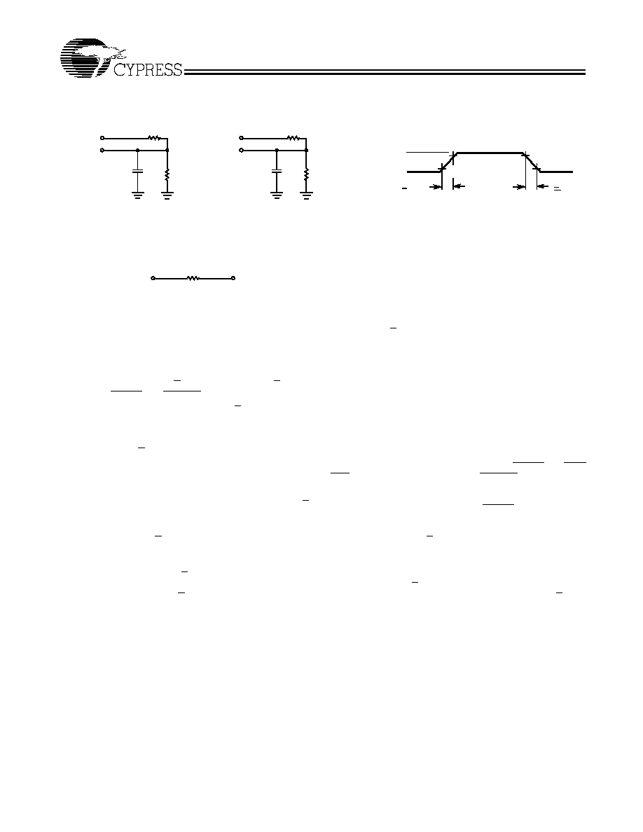
AC Test Loads and Waveforms
[4]
3.0V
5V
OUTPUT
R1 250
R2
167
50 pF
INCLUDING
JIG AND
SCOPE
GND
90%
10%
90%
10%
< 5 ns
< 5 ns
5V
OUTPUT
5pF
INCLUDING
JIG AND
SCOPE
(b) High Z Load
OUTPUT
2.0V
Equivalent to:
THÉ VENIN EQUIVALENT
100
R1 250
(a) Normal Load
R2
167
ALL INPUT PULSES
CY7C225A
Document #: 38-04001 Rev. **
Page 4 of 10
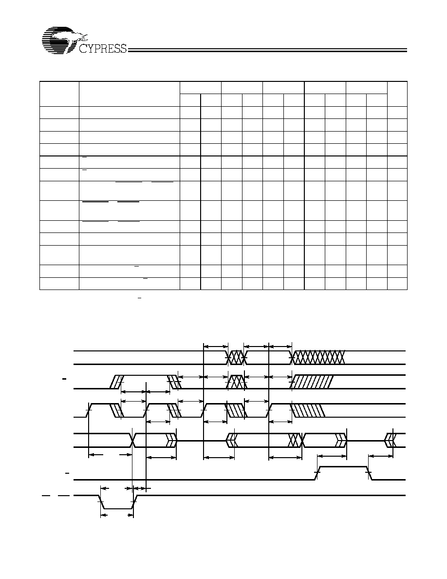
Switching Characteristics
Over the Operating Range
[3,4]
7C225A-18
7C225A-25
7C225A-30
7C225A-35
7C225A-40
Unit
Parameter
Description
Min.
Max.
Min.
Max.
Min.
Max.
Min.
Max.
Min.
Max.
t
SA
Address Set-Up to Clock HIGH
18
25
30
35
40
ns
t
HA
Address Hold from Clock HIGH
0
0
0
0
0
ns
t
CO
Clock HIGH to Valid Output
12
12
15
20
25
ns
t
PWC
Clock Pulse Width
10
10
15
20
20
ns
t
SES
E
S
Set-Up to Clock HIGH
10
10
10
10
10
ns
t
HES
E
S
Hold from Clock HIGH
0
0
5
5
5
ns
t
DP
, t
DC
Delay from PRESET or CLEAR
to Valid Output
20
20
20
20
20
ns
t
RP
, t
RC
PRESET or CLEAR Recovery to
Clock HIGH
15
15
20
20
20
ns
t
PWP
, t
PWC
PRESET or CLEAR Pulse Width
15
15
20
20
20
ns
t
COS
Valid Output from Clock HIGH
[7]
15
20
20
25
30
ns
t
HZC
Inactive Output from Clock
HIGH
[7]
15
20
20
25
30
ns
t
DOE
Valid Output from E LOW
15
20
20
25
30
ns
t
HZE
Inactive Output from E HIGH
15
20
20
25
30
ns
Note:
7.
Applies only when the synchronous (E
S
) function is used.
Switching Waveforms
[4]
t
DP
t
DC
t
CO
t
DOE
t
HZE
t
HZC
t
SA
t
HA
C225A-7
t
PWC
t
HES
t
PWC
t
PWC
t
PWC
t
PWC
t
PWC
t
SES
t
HA
t
CO
t
COS
O
0
-
O
7
A
0
-
A
10
PS or CLR
CP
E
S
E
t
RP
, t
RC
t
PWP
t
PWC
t
HES
t
SES
t
HES
t
SES
CY7C225A
Document #: 38-04001 Rev. **
Page 5 of 10
Programming Information
Programming support is available from Cypress as well as
from a number of third-party software vendors. For detailed
programming information, including a listing of software pack-
ages, please see the PROM Programming Information located
at the end of this section. Programming algorithms can be ob-
tained from any Cypress representative.
Table 1. Mode Selection
Pin Function
[8]
Read or Output Disable
A
8
- A
0
CP
E
S
CLR
E
PS
O
7
-
O
0
Mode
Other
A
8
- A
0
PGM
VFY
V
PP
E
PS
D
7
-
D
0
Read
A
8
- A
0
X
V
IL
V
IH
V
IL
V
IH
O
7
-
O
0
Output Disable
A
8
- A
0
X
V
IH
V
IH
X
V
IH
High Z
Output Disable
A
8
- A
0
X
X
V
IH
V
IH
V
IH
High Z
Clear
A
8
- A
0
X
V
IL
V
IL
V
IL
V
IH
Zeros
Preset
A
8
- A
0
X
V
IL
V
IH
V
IL
V
IL
Ones
Program
A
8
- A
0
V
ILP
V
IHP
V
PP
V
IHP
V
IHP
D
7
-
D
0
Program Verify
A
8
- A
0
V
IHP
V
ILP
V
PP
V
IHP
V
IHP
O
7
-
O
0
Program Inhibit
A
8
- A
0
V
IHP
V
IHP
V
PP
V
IHP
V
IHP
High Z
Intelligent Program
A
8
- A
0
V
ILP
V
IHP
V
PP
V
IHP
V
IHP
D
7
-
D
0
Blank Check
A
8
- A
0
V
IHP
V
ILP
V
PP
V
IHP
V
IHP
Zeros
Note:
8.
X = "don't care" but not to exceed V
CC
±5%.
Figure 1. Programming Pinouts.
1
2
3
4
5
6
7
8
9
10
11
12
16
17
18
19
20
24
23
22
21
13
14
A
8
A
7
A
6
A
5
A
4
A
3
A
2
A
1
A
0
D
0
D
1
D
2
GND
V
CC
D
7
D
6
D
4
D
5
D
3
15
PS
E
V
PP
VFY
PGM
28
4
5
6
7
8
9
10
3 2 1
27
1314151617
26
25
24
23
22
21
20
11
12
19
A
5
V CC
GND
A
6
A
7
D
3
D
1
D
0
18
D
4
D
5
NC
A
0
A
4
A
3
A
8
NC
NC
D
7
D
6
A
2
A
1
D
2
E
V
PP
VFY
PGM
NC
PS
DIP
LCC/PLCC
Top View
Top View
Document Outline
- CY7C225A
- Features
- Functional Description
- Selection Guide
- 18
- 25
- 30
- 35
- 40
- 12
- 12
- 15
- 20
- 25
- 90
- 90
- 90
- 90
- 120
- 120
- 120
- 120
- 0°C to +70°C
- 5V ± 10%
- -40°C to +85°C
- 5V ± 10%
- -55°C to +125°C
- 5V ± 10%
- 2.4
- V
- 0.4
- V
- 2.0
- V
- 0.8
- V
- -10
- +10
- mA
- -10
- +10
- mA
- -20
- -90
- mA
- 90
- mA
- 120
- 12
- 13
- V
- 50
- mA
- 3.0
- V
- 0.4
- V
- 10
- pF
- 10
- pF
- Notes:
- Note:
- Note:
- Note:
- 9. Most of these products are available in industrial temperature range. Contact a Cypress repres...
- MILITARY SPECIFICATIONS Group A Subgroup Testing
- DC Characteristics
- VOH
- 1, 2, 3
- VOL
- 1, 2, 3
- VIH
- 1, 2, 3
- VIL
- 1, 2, 3
- IIX
- 1, 2, 3
- IOZ
- 1, 2, 3
- ICC
- 1, 2, 3
- tSA
- 7, 8, 9, 10, 11
- tHA
- 7, 8, 9, 10, 11
- tCO
- 7, 8, 9, 10, 11
- tDP
- 7, 8, 9, 10, 11
- tRP
- 7, 8, 9, 10, 11
- **
- 113858
- 03/06/02
- DSG
- Change from Spec number: 38-00228 to 38-04001