 | ÐлекÑÑоннÑй компоненÑ: CY7C263 | СкаÑаÑÑ:  PDF PDF  ZIP ZIP |
Untitled Document
8K x 8 Power-Switched and Reprogrammable PROM
CY7C261
CY7C263/CY7C264
Cypress Semiconductor Corporation
·
3901 North First Street
·
San Jose
·
CA 95134
·
408-943-2600
Document #: 38-04010 Rev. **
Revised March 4, 2002
Features
· CMOS for optimum speed/power
· Windowed for reprogrammability
· High speed
-- 20 ns (commercial)
-- 25 ns (military)
· Low power
-- 660 mW (commercial)
-- 770 mW (military)
· Super low standby power (7C261)
-- Less than 220 mW when deselected
-- Fast access: 20 ns
· EPROM technology 100% programmable
· Slim 300-mil or standard 600-mil packaging available
· 5V
±
10% V
CC
, commercial and military
· Capable of withstanding greater than 2001V static dis-
charge
· TTL-compatible I/O
· Direct replacement for bipolar PROMs
Functional Description
The CY7C261, CY7C263, and CY7C264 are high-perfor-
mance 8192-word by 8-bit CMOS PROMs. When deselected,
the 7C261 automatically powers down into a low-power stand-
by mode. It is packaged in a 300-mil-wide package. The 7C263
and 7C264 are packaged in 300-mil-wide and 600-mil-wide
packages respectively, and do not power down when deselect-
ed. The reprogrammable packages are equipped with an era-
sure window; when exposed to UV light, these PROMs are
erased and can then be reprogrammed. The memory cells uti-
lize proven EPROM floating-gate technology and byte-wide in-
telligent programming algorithms.
The CY7C261, CY7C263, and CY7C264 are plug-in replace-
ments for bipolar devices and offer the advantages of lower
power, superior performance and programming yield. The
EPROM cell requires only 12.5V for the supervoltage and low
current requirements allow for gang programming. The
EPROM cells allow for each memory location to be tested
100%, as each location is written into, erased, and repeatedly
exercised prior to encapsulation. Each PROM is also tested for
AC performance to guarantee that after customer program-
ming the product will meet DC and AC specification limits.
Read is accomplished by placing an active LOW signal on CS.
The contents of the memory location addressed by the ad-
dress line (A
0
-
A
12
) will become available on the output lines
(O
0
-
O
7
).
For an 8K x 8 Registered PROM, see theCY7C265.
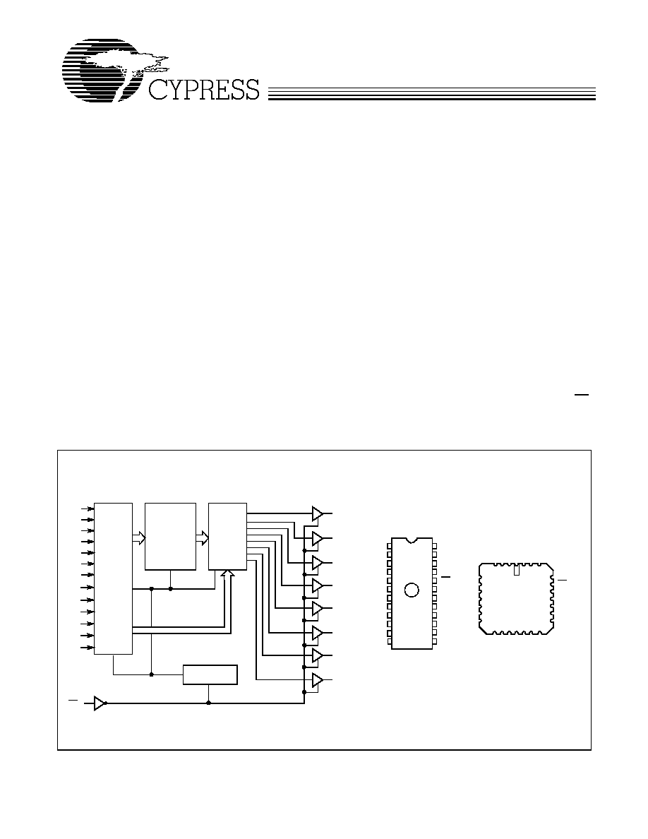
Logic Block Diagram
Pin Configurations
O
7
O
6
O
5
O
4
O
3
O
2
O
1
O
0
ADDRESS
DECODER
PROGRAM
MABLE
ARRAY
COLUMN
MULTI
PLEXER
POWER DOWN
(7C261)
A
0
A
1
A
2
A
3
A
4
A
5
A
6
A
8
A
9
A
10
A
11
A
12
CS
GND
1
2
3
4
5
6
7
8
9
10
11
14
15
16
20
19
18
17
21
24
23
22
Top View
DIP/Flatpack
A
6
A
5
A
4
A
3
A
2
A
1
A
0
O
0
A
7
O
3
V
CC
A
8
A
9
A
10
O
7
O
6
O
5
O
4
CS
O
2
12
13
O
1
A
12
A
11
28
4
5
6
7
8
9
10
3 2 1
27
1314151617
26
25
24
23
22
21
20
11
12
19
A
5
V
CC
GND
A
6
A
7
O
3
O
1
O
0
Top View
18
O
4
O
5
NC
A
0
A
4
A
3
A
10
NC
A
8
A
9
NC
NC
CS
A
11
O
7
O
6
7C261
7C263
7C264
7C261
7C263
A
7
A
2
A
1
A
12
O
2
COLUMN
ADDRESS
ROW
ADDRESS
LCC/PLCC (Opaque Only)
CY7C261
CY7C263/CY7C264
Document #: 38-04010 Rev. **
Page 2 of 16
Maximum Ratings
(Above which the useful life may be impaired. For user guide-
lines, not tested.)
Storage Temperatures .................................65
°
C to+150
°
C
Ambient Temperature with
Power Applied..............................................55
°
C to+125
°
C
Supply Voltage to Ground Potential
(Pin 24 to Pin 12) ............................................ 0.5V to+7.0V
DC Voltage Applied to Outputs
in High Z State ................................................ 0.5V to+7.0V
DC Input Voltage........................................... 3.0V to + 7.0V
DC Program Voltage
(Pin 19 DIP, Pin 23 LCC) ..............................................13.0V
Static Discharge Voltage............................................>2001V
(per MIL-STD-883, Method 3015)
Latch-Up Current ..................................................... >200 mA
UV Exposure ................................................ 7258 Wsec/cm
2
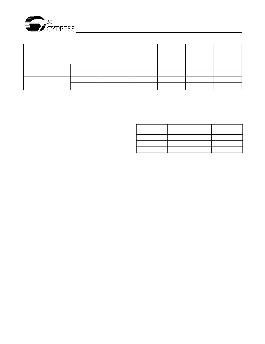
Selection Guide
7C261-20
7C263-20
7C264-20
7C261-25
7C263-25
7C264-25
7C261-35
7C263-35
7C264-35
7C261-45
7C263-45
7C264-45
7C261-55
7C263-55
7C264-55
Maximum Access Time (ns)
20
25
35
45
55
Maximum Operating
Current (mA)
Commercial
120
120
100
100
100
Military
140
120
120
120
Maximum Standby
Current (mA)
(7C261 only)
Commercial
40
40
30
30
30
Military
40
30
30
30
Operating Range
Range
Ambient
Temperature
V
CC
Commercial
0
°
C to + 70
°
C
5V
±
10%
Industrial
[1]
40
°
C to + 85
°
C
5V
±
10%
Military
[2]
55
°
C to + 125
°
C
5V
±
10%
Notes:
1.
See the Ordering Information section regarding industrial temperature
range specification.
2.
T
A
is the "instant on" case temperature.
CY7C261
CY7C263/CY7C264
Document #: 38-04010 Rev. **
Page 3 of 16
]]
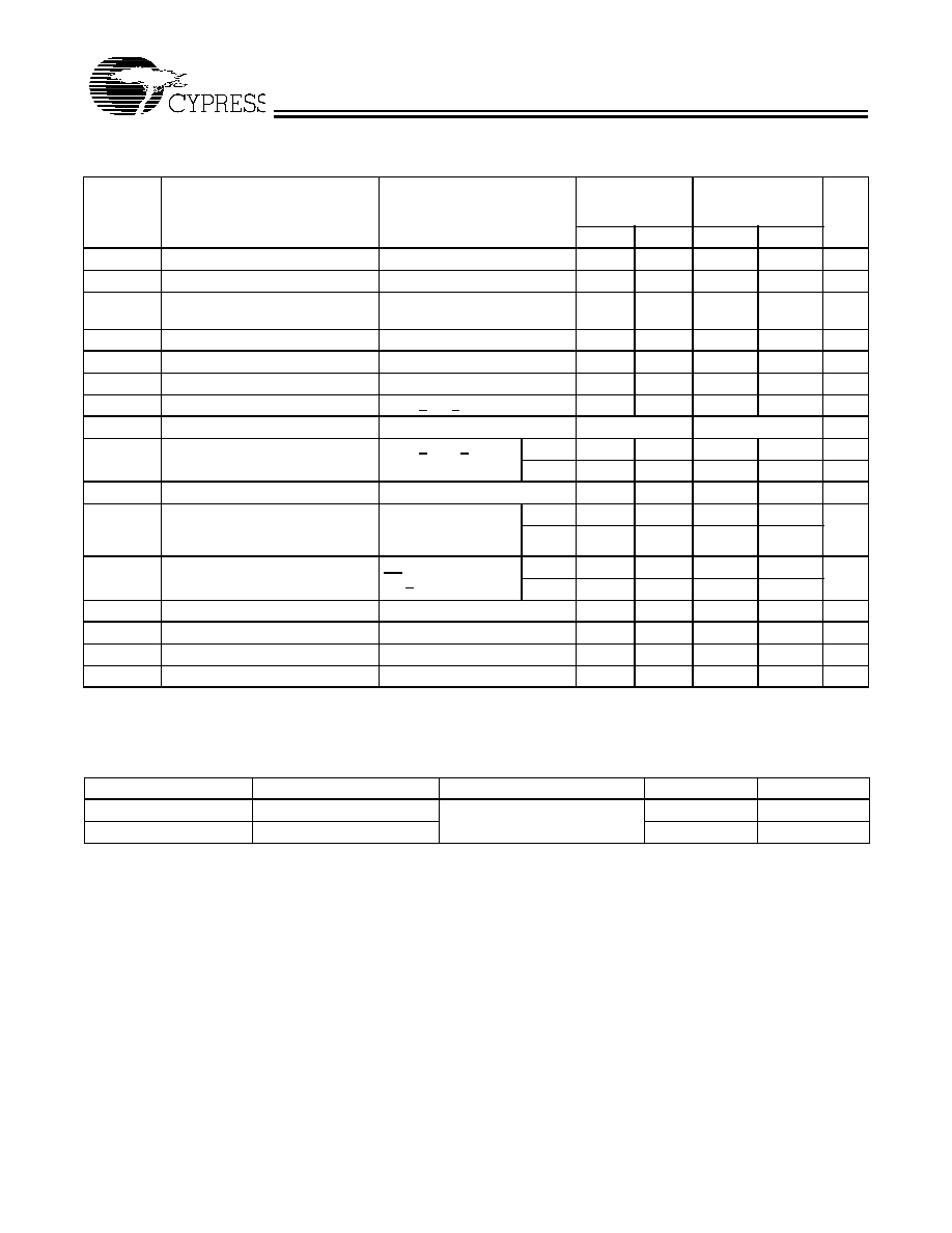
Electrical Characteristics
Over the Operating Range
[3,4]
7C261-20, 25
7C263-20, 25
7C264-20, 25
7C261-35, 45, 55
7C263-35, 45, 55
7C264-35, 45, 55
Parameter
Description
Test Conditions
Min.
Max.
Min.
Max.
Unit
V
OH
Output HIGH Voltage
V
CC
= Min., I
OH
= 2.0 mA
2.4
V
V
OH
Output HIGH Voltage
V
CC
= Min., I
OH
= 4.0 mA
2.4
V
V
OL
Output LOW Voltage
V
CC
= Min., I
OL
= 8 mA
(6 mA Mil)
0.4
V
V
OL
Output LOW Voltage
V
CC
= Min., I
OL
= 16 mA
0.4
V
V
IH
Input HIGH Level
2.0
2.0
V
V
IL
Input LOW Level
0.8
0.8
V
I
IX
Input Current
GND < V
IN
< V
CC
10
+10
10
+10
µ
A
V
CD
Input Diode Clamp Voltage
Note 4
Note 4
I
OZ
Output Leakage Current
GND <V
OUT
< V
CC
Output Disabled
Com'l
10
+10
10
+10
µ
A
Mil
40
+40
40
+40
µ
A
I
OS
Output Short Circuit Current
[5]
V
CC
= Max., V
OUT
= GND
20
90
20
90
mA
I
CC
Power Supply Current
V
CC
= Max.,
f = Max.
I
OUT
= 0 mA
Com'l
120
100
mA
Mil
140
120
I
SB
Standby Supply Current (7C261)
V
CC
= Max.,
CS > V
IH
Com'l
40
30
mA
Mil
40
30
V
PP
Programming Supply Voltage
12
13
12
13
V
I
PP
Programming Supply Current
50
50
mA
V
IHP
Input HIGH Programming Voltage
4.75
4.75
V
V
ILP
Input LOW Programming Voltage
0.4
0.4
V
Notes:
3.
See the last page of this specification for Group A subgroup testing information.
4.
See the "Introduction to CMOS PROMs" section of the Cypress Data Book for general information on testing.
5.
For test purposes, not more than one output at a time should be shorted. Short circuit test duration should not exceed 30 seconds.]
Capacitance
[4]
Parameter
Description
Test Conditions
Max.
Unit
C
IN
Input Capacitance
T
A
= 25
°
C, f = 1 MHz,
V
CC
= 5.0V
10
pF
C
OUT
Output Capacitance
10
pF
CY7C261
CY7C263/CY7C264
Document #: 38-04010 Rev. **
Page 4 of 16
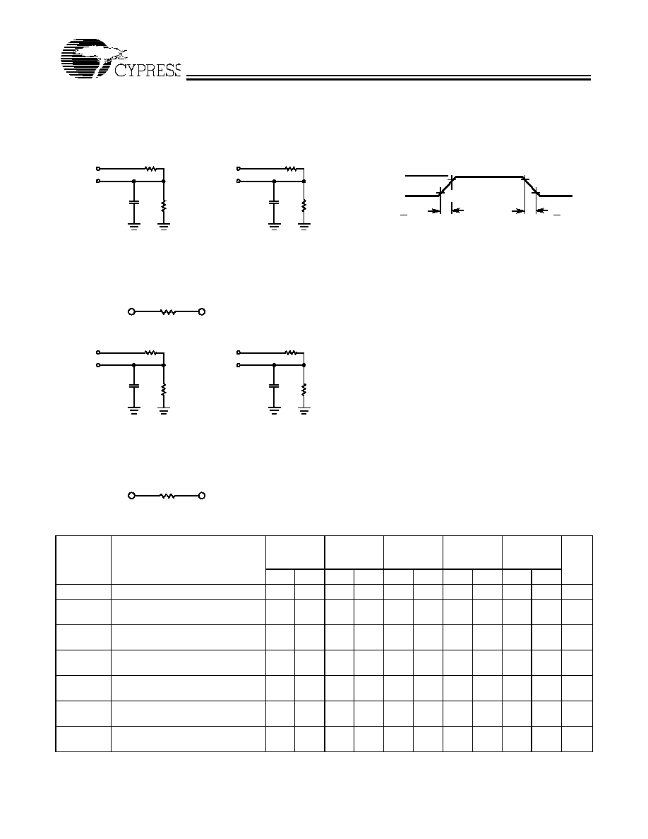
AC Test Loads and Waveforms
[4]
Switching Characteristics
Over the Operating Range
[2,3,4
]
7C261-20
7C263-20
7C264-20
7C261-25
7C263-25
7C264-25
7C261-35
7C263-35
7C264-35
7C261-45
7C263-45
7C264-45
7C261-55
7C263-55
7C264-55
Parameter
Description
Min.
Max.
Min.
Max.
Min.
Max.
Min.
Max.
Min.
Max.
Unit
t
AA
Address to Output Valid
20
25
35
45
55
ns
t
HZCS1
Chip Select Inactive to High Z
(7C263 and 7C264)
12
12
20
30
35
ns
t
HZCS2
Chip Select Inactive to High Z
(7C261)
20
25
35
45
55
ns
t
ACS1
Chip Select Active to Output Valid
(7C263 and 7C264)
12
12
20
30
35
ns
t
ACS2
Chip Select Active to Output Valid
(7C261)
20
25
35
45
55
ns
t
PU
Chip Select Active to Power-Up
(7C261)
0
0
0
0
0
ns
t
PD
Chip Select Inactive to
Power-Down (7C261)
20
25
35
45
55
ns
R2 333
(403
MIL)
3.0V
5V
OUTPUT
R1 500
(658
MIL)
30 pF
INCLUDING
JIG AND
SCOPE
GND
90%
10%
90%
10%
5 ns
5 ns
5V
OUTPUT
5 pF
INCLUDING
JIG AND
SCOPE
(a) Normal Load
(b) High Z Load
OUTPUT
R
TH
200
(250
MIL)
5V
OUTPUT
5V
OUTPUT
R1250
30pF
INCLUDING
JIG AND
SCOPE
5 pF
INCLUDING
JIG AND
SCOPE
(c) Normal Load
(d) High Z Load
OUTPUT
2.0V
R
TH
100
R1 250
R1 500
(658
MIL)
R2 333
(403
MIL)
R2167
R2167
2.0V(1.9VMIL)
Test Load for -20 through -30 speeds
Test Load for -35 through -55 speeds
Equivalent to:
THÉ VENIN EQUIVALENT
Equivalent to:
THÉ VENIN EQUIVALENT
CY7C261
CY7C263/CY7C264
Document #: 38-04010 Rev. **
Page 5 of 16
Erasure Characteristics
Wavelengths of light less than 4000 angstroms begin to erase
the devices in the windowed package. For this reason, an
opaque label should be placed over the window if the PROM
is exposed to sunlight or fluorescent lighting for extended pe-
riods of time.
The recommended dose of ultraviolet light for erasure is a
wavelength of 2537 angstroms for a minimum dose (UV inten-
sity multiplied by exposure time) of 25 Wsec/cm
2
. For an ultra-
violet lamp with a 12 mW/cm
2
power rating, the exposure time would
be approximately 35 minutes. The 7C261 or 7C263 needs to
be within 1 inch of the lamp during erasure. Permanent dam-
age may result if the PROM is exposed to high-intensity UV
light for an extended period of time. 7258 Wsec/cm
2
is the
recommended maximum dosage.
Operating Modes
Read
Read is the normal operating mode for programmed device. In
this mode, all signals are normal TTL levels. The PROM is
addressed with a 13-bit field, a chip select, (active LOW), is
applied to the CS pin, and the contents of the addressed location
appear on the data out pins.
Program, Program Inhibit, Program Verify
These modes are entered by placing a high voltage V
PP
on pin
19, with pins 18 and 20 set to V
ILP
. In this state, pin 21 becomes a
latch signal, allowing the upper 5 address bits to be latched into an
onboard register, pin 22 becomes an active LOW program (PGM)
signal and pin 23 becomes an active LOW verify (VFY) signal. Pins
22 and 23 should never be active LOW at the same time. The PRO-
GRAM mode exists when PGM is LOW, and VFY is HIGH. The verify
mode exists when the reverse is true, PGM HIGH and VFY LOW and
the program inhibit mode is entered with both PGM and VFY HIGH.
Program inhibit is specifically provided to allow data to be placed on
and removed from the data pins without conflict
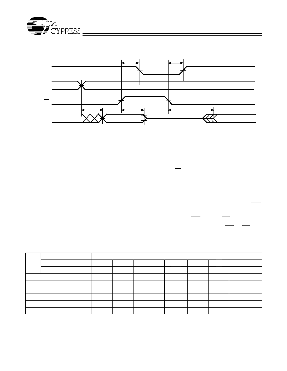
Switching Waveforms
[4]
t
AA
V
CC
SUPPLY
CURRENT
A
0
- A
12
ADDRESS
CS
t
PU
O
0
- O
7
t
HZCS
t
ACS
50%
50%
t
PD
Table 1. Mode Selection
Pin Function
[6, 7]
Read or Output Disable
A
12
A
11
A
10
A
9
A
8
CS
O
7
O
0
Mode
Program
NA
V
PP
LATCH
PGM
VFY
CS
D
7
D
0
Read
A
12
A
11
A
10
A
9
A
8
V
IL
O
7
O
0
Output Disable
A
12
A
11
A
10
A
9
A
8
V
IH
High Z
Program
V
ILP
V
PP
V
ILP
V
ILP
V
IHP
V
ILP
D
7
D
0
Program Inhibit
V
ILP
V
PP
V
ILP
V
IHP
V
IHP
V
ILP
High Z
Program Verify
V
ILP
V
PP
V
ILP
V
IHP
V
ILP
V
ILP
O
7
O
0
Blank Check
V
ILP
V
PP
V
ILP
V
IHP
V
ILP
V
ILP
O
7
O
0
Notes:
6.
X = "don't care" but not to exceed V
CC
±
5%.
7.
Addresses A
8
-A
12
must be latched through lines A
0
-A
4
in programming modes.
Document Outline