Untitled Document

8K x 8 Registered PROM
CY7C265
Cypress Semiconductor Corporation
·
3901 North First Street
·
San Jose
·
CA 95134
·
408-943-2600
Document #: 38-04012 Rev. **
Revised March 14, 2002
65
Features
· CMOS for optimum speed/power
· High speed (commercial and military)
-- 15 ns address set-up
-- 12 ns clock to output
· Low power
-- 660 mW (commercial)
-- 770 mW (military)
· On-chip edge-triggered registers
-- Ideal for pipelined microprogrammed systems
· EPROM technology
-- 100% programmable
-- Reprogrammable (7C265W)
· 5V
±
10% V
CC
, commercial and military
· Capable of withstanding >2001V static discharge
· Slim 28-pin, 300-mil plastic or hermetic DIP
Functional Description
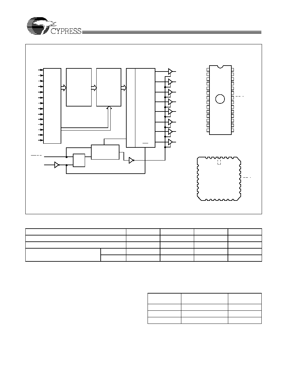
The CY7C265 is a 8192 x 8 registered PROM. It is organized
as 8,192 words by 8 bits wide, and has a pipeline output reg-
ister. In addition, the device features a programmable initialize
byte that may be loaded into the pipeline register with the ini-
tialize signal. The programmable initialize byte is the 8,193rd
byte in the PROM and its value is programmed at the time of
use.
Packaged in 28 pins, the PROM has 13 address signals (A
0
through A
12
), 8 data out signals (O
0
through O
7
), E/I (enable
or initialize), and CLOCK.
CLOCK functions as a pipeline clock, loading the contents of
the addressed memory location into the pipeline register on
each rising edge. The data will appear on the outputs if they
are enabled. One pin on the CY7C265 is programmed to per-
form either the enable or the initialize function.
If the asynchronous enable (E) is being used, the outputs may
be disabled at any time by switching the enable to a logic
HIGH, and may be returned to the active state by switching the
enable to a logic LOW.
If the synchronous enable (ES) is being used, the outputs will
go to the OFF or high-impedance state upon the next positive
clock edge after the synchronous enable input is switched to a
HIGH level. If the synchronous enable pin is switched to a logic
LOW, the subsequent positive clock edge will return the output
to the active state. Following a positive clock edge, the address
and synchronous enable inputs are free to change since no
change in the output will occur until the next LOW-to-HIGH
transition of the clock. This unique feature allows the CY7C265
decoders and sense amplifiers to access the next location
while previously addressed data remains stable on the outputs.
If the E/I pin is used for INIT (asynchronous), then the outputs
are permanently enabled. The initialize function is useful dur-
ing power-up and time-out sequences, and can facilitate im-
plementation of other sophisticated functions such as a built-in
"jump start" address. When activated, the initialize control in-
put causes the contents of a user programmed 8193rd 8-bit
word to be loaded into the on-chip register. Each bit is pro-
grammable and the initialize function can be used to load any
desired combination of 1's and 0's into the register. In the un-
programmed state, activating INIT will generate a register
clear (all outputs LOW). If all the bits of the initialize word are
programmed to be a 1, activating INIT performs a register pre-
set (all outputs HIGH).
Applying a LOW to the INIT input causes an immediate load of
the programmed initialize word into the pipeline register and
onto the outputs. The INIT LOW disables clock and must return
HIGH to enable clock independent of all other inputs, including
the clock.
CY7C265
Document #: 38-04012 Rev. **
Page 2 of 13
F
Maximum Ratings
(Above which the useful life may be impaired. For user guide-
lines, not tested.)
Storage Temperature .................................65
°
C to +150
°
C
Ambient Temperature with
Power Applied.............................................55
°
C to +125
°
C
Supply Voltage to Ground Potential ............... 0.5V to +7.0V
DC Voltage Applied to Outputs
in High Z State ............................................... 0.5V to +7.0V
DC Input Voltage............................................ 3.0V to +7.0V
DC Program Voltage .....................................................13.0V
UV Exposure.................................................7258 Wsec/cm
2
Static Discharge Voltage ........................................... >2001V
(per MIL-STD-883, Method 3015)
Latch-Up Current ..................................................... >200 mA
Logic Block Diagram
Pin Configurations
Top View
LCC/PLCC (Opaque Only)
1
2
3
4
5
6
7
8
9
10
11
12
16
17
18
19
20
24
23
22
21
13
14
25
28
27
26
Top View
DIP/Flatpack
15
7C265
A
7
A
6
A
5
A
4
A
3
A
2
GND
CLK
A
1
A
0
O
0
O
1
O
2
GND
V
CC
A
8
A
9
A
10
A
11
A
12
E/E
S
,I
GND
GND
O
7
O
6
O
4
O
5
O
3
O
7
O
6
O
5
O
4
O
3
O
2
O
1
O
0
A
12
A
11
A
10
A
9
A
8
A
7
A
6
A
5
COLUMN
MULTIPLEXER
A
4
A
3
A
2
A
1
PROGRAMMABLE
MULTIPLEXER
ADDRESS
DECODER
PROGRAMMABLE
ARRAY
8-BIT
EDGE-
TRIGGERED
REGISTER
CLK
INIT/E/E
S
CLK
P
R
O
G
R
AM
M
A
BL
E
INIT
IA
LIZ
E
W
O
RD
D
C
O
28
4
5
6
7
8
9
10
3
2 1
27
13 14 15 16 17
26
25
24
23
22
21
20
11
12
19
O
0
18
A
0
A
1
A
3
A
2
A
10
GND
A
11
A
12
GND
O
7
GND
CLK
E/E
S
,I
A
4
A
5
A
6
A
7
V
CC
A
8
A
9
O
1
O
2
GND O
3
O
4
O
5
O
6
A
5
A
0
ROW
ADDRESS
COLUMN
ADDRESS
Selection Guides
7C26515
7C26525
7C26540
7C26550
Minimum Address Set-Up Time (ns)
15
25
40
50
Maximum Clock to Output (ns)
12
15
20
25
Maximum Operating Current (mA)
Com'l
120
120
100
80
Mil
140
140
120
Operating Range
Range
Ambient
Temperature
V
CC
Commercial
0
°
C to +70
°
C
5V
±
10%
Industrial
[1]
40
°
C to +85
°
C
5V
±
10%
Military
[2]
55
°
C to +125
°
C
5V
±
10%
Notes:
1.
Contact a Cypress representative for industrial temperature range spec-
ifications.
2.
T
A
is the "instant on" case temperature.
CY7C265
Document #: 38-04012 Rev. **
Page 3 of 13
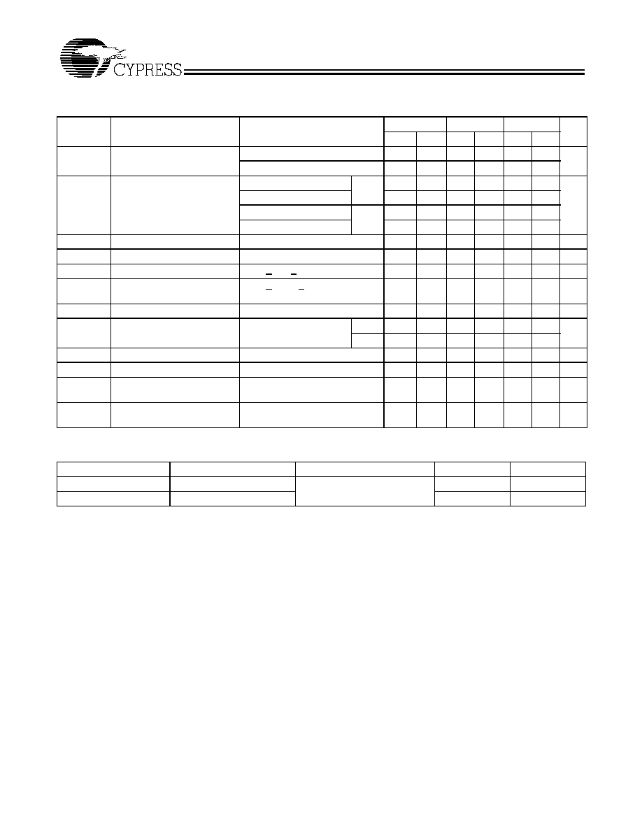
Electrical Characteristics
Over the Operating Range
[3]
7C265-15, 25
7C265-40
7C265-50
Parameter
Description
Test Conditions
Min.
Max.
Min.
Max. Min. Max. Unit
V
OH
Output HIGH Voltage
V
CC
= Min., I
OH
= 2.0 mA
2.4
V
V
CC
= Min., I
OH
= 4.0 mA
2.4
2.4
V
OL
Output LOW Voltage
V
CC
= Min., I
OL
= 8.0 mA Com'l
0.4
V
V
CC
= Min., I
OL
= 12.0 mA
0.4
0.4
V
CC
= Min., I
OL
= 6.0 mA Mil
0.4
V
CC
= Min., I
OL
= 8.0 mA
0.4
V
IH
Input HIGH Voltage
2.0
2.0
2.0
V
V
IL
Input LOW Voltage
0.8
0.8
0.8
V
I
IX
Input Load Current
GND < V
IN
< V
CC
10
+10
10
+10
10
+10
µ
A
I
OZ
Output Leakage Current
GND < V
OUT
< V
CC
,
Output Disabled
40
+40
40
+40
40
+40
µ
A
I
OS
[4]
Output Short Circuit Current
V
CC
= Max., V
OUT
= GND
90
90
90
mA
I
CC
V
CC
Operating Supply
Current
V
CC
= Max., I
OUT
= 0 mA Com'l
120
100
80
mA
Mil
140
120
V
PP
Programming Supply Voltage
12
13
12
13
12
13
V
I
PP
Programming Supply Current
50
50
50
mA
V
IHP
Input HIGH Programming
Voltage
3.0
3.0
3.0
V
V
ILP
Input LOW Programming
Voltage
0.4
0.4
0.4
V
Capacitance
[5]
Parameter
Description
Test Conditions
Max.
Unit
C
IN
Input Capacitance
T
A
= 25
°
C, f = 1 MHz,
V
CC
= 5.0V
10
pF
C
OUT
Output Capacitance
10
pF
Notes:
3.
See the last page of this specification for Group A subgroup testing information.
4.
For test purposes, not more than one output at a time should be shorted. Short circuit test duration should not exceed 30 seconds.
5.
See Introduction to CMOS PROMs in this Data Book for general information on testing.
CY7C265
Document #: 38-04012 Rev. **
Page 4 of 13
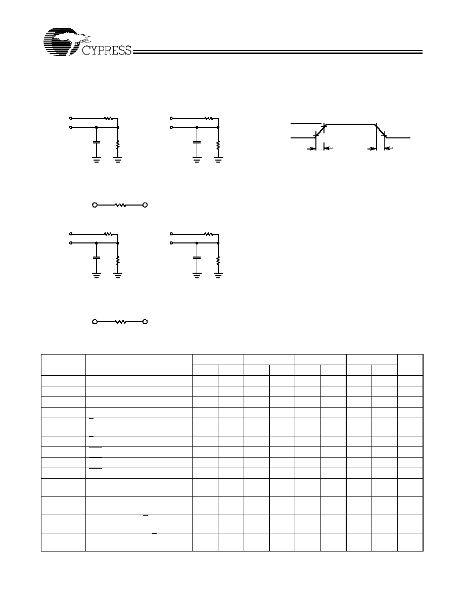
AC Test Loads and Waveforms
R2 333
(403
MIL)
3.0V
5V
OUTPUT
R1 500
(658
MIL)
30 pF
INCLUDING
JIG AND
SCOPE
GND
90%
10%
90%
10%
5 ns
5 ns
5V
OUTPUT
5 pF
INCLUDING
JIG AND
SCOPE
(a) Normal Load
(b) High Z Load
OUTPUT
R
TH
200
5V
OUTPUT
5V
OUTPUT
R1 250
30 pF
INCLUDING
JIG AND
SCOPE
5 pF
INCLUDING
JIG AND
SCOPE
(c) Normal Load
(d) High Z Load
OUTPUT
2.0V
R
TH
100
R1 250
R1 500
(658
MIL)
R2 333
(403
MIL)
R2 167
R2 167
250
MIL
Equivalent to:
THÉ VENIN EQUIVALENT
Equivalent to:
THÉ VENIN EQUIVALENT
Test Load for -15 through -25 speeds
Test Load for -40 through -50 speeds
Switching Characteristics
Over the Operating Range
[3, 5]
7C265-15
7C265-25
7C265-40
7C265-50
Parameter
Description
Min.
Max.
Min.
Max.
Min.
Max.
Min.
Max.
Unit
t
AS
Address Set-Up to Clock
15
25
40
50
ns
t
HA
Address Hold from Clock
0
0
0
0
ns
t
CO
Clock to Output Valid
12
15
20
25
ns
t
PWC
Clock Pulse Width
12
15
15
20
ns
t
SES
E
S
Set-Up to Clock
(Sync. Enable Only)
12
15
15
15
ns
t
HES
E
S
Hold from Clock
5
5
5
5
ns
t
DI
INIT to Output Valid
15
18
25
35
ns
t
RI
INIT Recovery to Clock
12
15
20
25
ns
t
PWI
INIT Pulse Width
12
15
25
35
ns
t
COS
Output Valid from Clock
(Sync. Mode)
12
15
20
25
ns
t
HZC
Output Inactive from Clock
(Sync. Mode)
12
15
20
25
ns
t
DOE
Output Valid from E LOW
(Async. Mode)
12
15
20
25
ns
t
HZE
Output Inactive from E HIGH
(Async. Mode)
12
15
20
25
ns
CY7C265
Document #: 38-04012 Rev. **
Page 5 of 13
Erasure Characteristics
Wavelengths of light less than 4000 angstroms begin to erase
the 7C265 in the windowed package. For this reason, an
opaque label should be placed over the window if the PROM
is exposed to sunlight or fluorescent lighting for extended pe-
riods of time.
The recommended dose of ultraviolet light for erasure is a
wavelength of 2537 angstroms for a minimum dose (UV inten-
sity · exposure time) of 25 Wsec/cm
2
. For an ultraviolet lamp
with a 12 mW/cm
2
power rating the exposure time would be
approximately 45 minutes. The 7C265 needs to be within one
inch of the lamp during erasure. Permanent damage may re-
sult if the PROM is exposed to high-intensity UV light for an
extended period of time. 7258 Wsec/cm
2
is the recommended
maximum dosage.
Control Byte
00
Asynchronous output enable (default condition)
01
Synchronous output enable
02
Asynchronous initialize
Programming Modes
The 7C265 offers a limited selection of programmed architec-
tures. Programming these features should be done with a sin-
gle 10-ms-wide pulse in place of the intelligent algorithm,
mainly because these features are verified operationally, not
with the VFY pin. Architecture programming is implemented by
applying the supervoltage to two additional pins during pro-
gramming. In programming the 7C265 architecture, VPP is ap-
plied to pins 3, 9, and 22. The choice of a particular mode
depends on the states of the other pins during programming,
so it is important that the condition of the other pins be met as
set forth in the mode table. The considerations that apply with
respect to power-up and power-down during intelligent pro-
gramming also apply during architecture programming. Once
the supervoltages have been established and the correct logic
states exist on the other device pins, programming may begin.
Programming is accomplished by pulling PGM from HIGH to
LOW and then back to HIGH with a pulse width equal to 10 ms.
Switching Waveform
t
HZC
t
PWC
t
HES
VALID DATA
t
COS
t
CO
t
PWI
t
DI
ADDRESS
CLOCK
SYNCHRONOUS
ENABLE
(PROGRAMMABLE)
ASYNCHRONOUS INIT
(PROGRAMMABLE)
OUTPUT
ASYNCHRONOUS
ENABLE
t
HZE
t
SES
t
AH
t
AS
t
DOE
t
RI
Bit Map Data
Programmer Address (Hex.)
RAM Data
Decimal
Hex
Contents
0
.
.
8191
8192
8193
0
.
.
1FFF
2000
2001
Data
.
.
Data
INIT Byte
Control Byte
Document Outline