Untitled Document
32K x 8 Power Switched and
Reprogrammable PROM
CY7C271
CY7C274
Cypress Semiconductor Corporation
·
3901 North First Street
·
San Jose
·
CA 95134
·
408-943-2600
Document #: 38-04008 Rev. **
Revised March 4, 2002
74
Features
· CMOS for optimum speed/power
· Windowed for reprogrammability
· High speed
-- 30 ns (commercial)
-- 35 ns (military)
· Low power
-- 660 mW (commercial)
-- 715 mW (military)
· Super low standby power
-- Less than 165 mW when deselected
· EPROM technology 100% programmable
· Slim 300-mil package (7C271)
· Direct replacement for bipolar PROMs
· Capable of withstanding >2001V static discharge
Functional Description
The CY7C271 and CY7C274 are high-performance
32,768-word by 8-bit CMOS PROMs. When disabled (CE
HIGH), the 7C271/7C274 automatically powers down into a
low-power stand-by mode. The CY7C271 is packaged in the
300-mil slim package. The CY7C274 is packaged in the indus-
try standard 600-mil package. Both the 7C271 and 7C274 are
available in a cerDIP package equipped with an erasure win-
dow to provide for reprogrammability. When exposed to UV
light, the PROM is erased and can be reprogrammed. The
memory cells utilize proven EPROM floating gate technology
and byte-wide intelligent programming algorithms.
The CY7C271 and CY7C274 offer the advantage of lower
power, superior performance, and programming yield. The
EPROM cell requires only 12.5V for the super voltage, and low
current requirements allow for gang programming. The
EPROM cells allow each memory location to be tested 100%
because each location is written into, erased, and repeatedly
exercised prior to encapsulation. Each PROM is also tested for
AC performance to guarantee that after customer program-
ming, the product will meet DC and AC specification limits.
Reading the 7C271 is accomplished by placing active LOW
signals on CS
1
and CE, and an active HIGH on CS
2
. Reading the
7C274 is accomplished by placing active LOW signals on OE and
CE. The contents of the memory location addressed by the address
lines (A
0
-
A
14
) will become available on the output lines (O
0
-
O
7
).
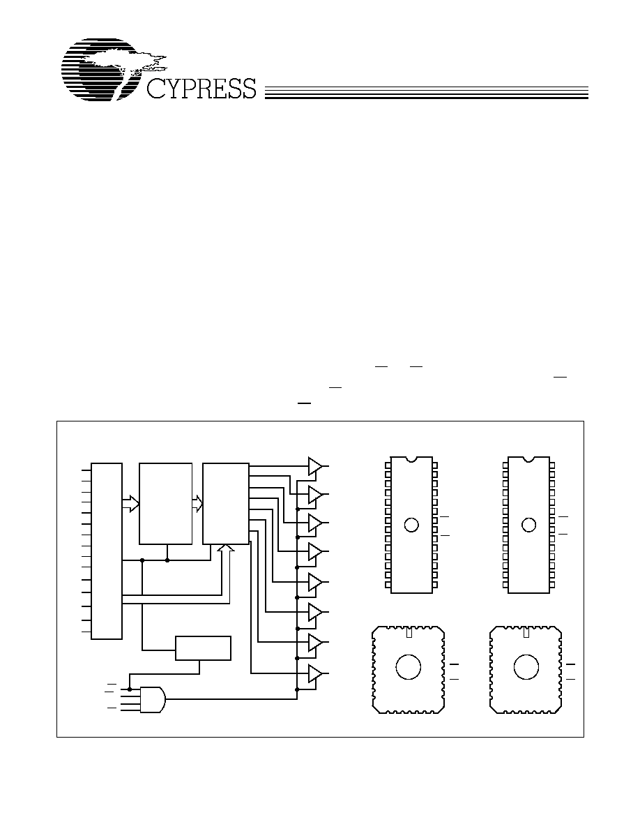
LogicBlockDiagram
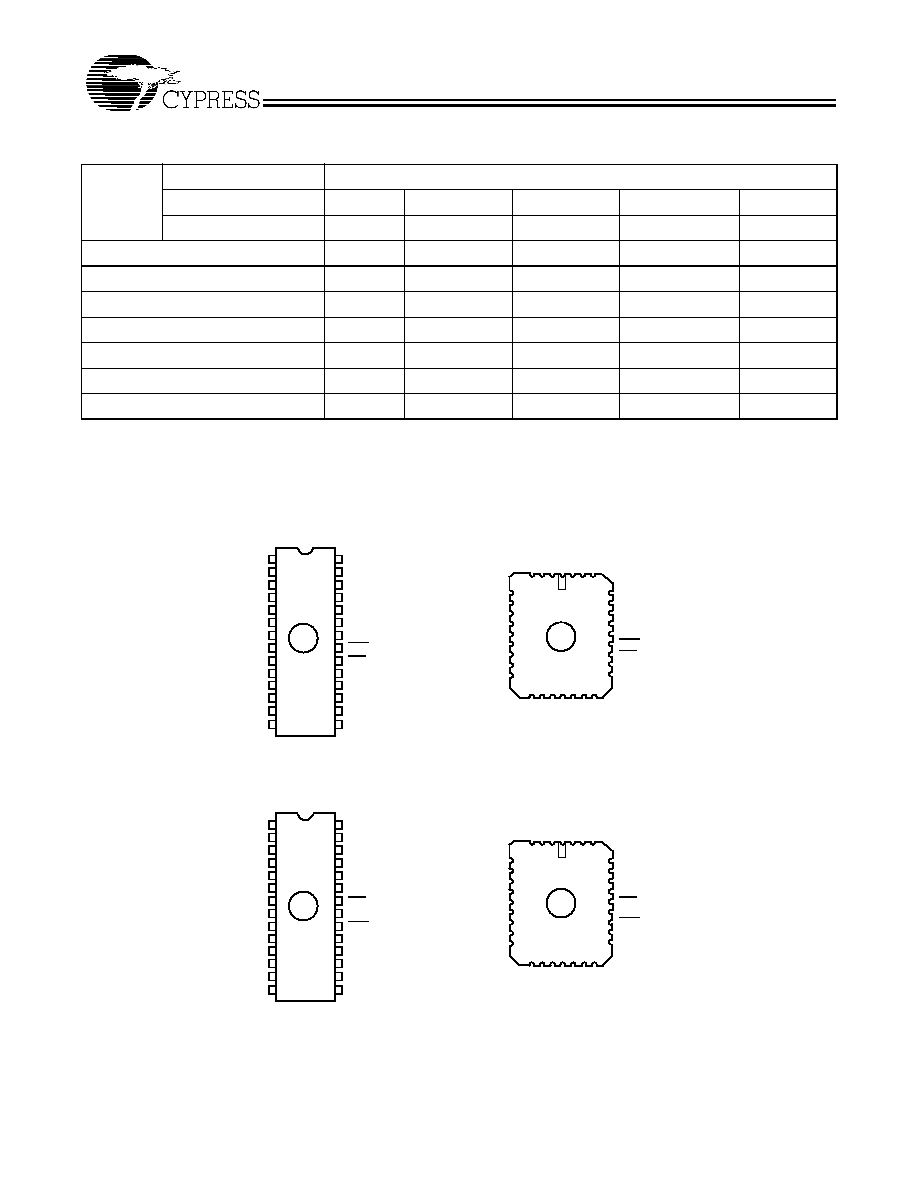
Pin Configurations
1
2
3
4
5
6
7
8
9
10
11
12
16
17
18
19
20
24
23
22
21
13
14
25
28
27
26
A
8
A
7
A
6
A
5
A
4
A
3
A
2
A
1
A
0
O
0
O
1
O
2
GND
V
CC
A
11
A
12
A
13
O
7
O
6
O
4
O
5
O
3
A
12
A
11
A
9
A
8
A
7
A
6
A
5
A
4
A
3
A
2
A
1
A
0
POWERDOWN
O
7
O
6
O
5
O
4
O
3
O
2
O
1
O
0
CE
256 x 1024
PROGRAMABLE
ARRAY
8 x 1 OF 128
MULTIPLEXER
12
31
4
5
6
7
8
9
10
3 2 1
30
13
14151617
26
25
24
23
22
21
11
V CC
A
5
A
4
A
3
A
2
A
6
A
1
A
13
A
14
O
7
O
6
O
4
GND
A
12
A
7
A
8
O
3
O
1
181920
27
28
29
32
NC
O
5
NC
15
A
10
A
13
(7C271) CS
1
(7C274) OE
A
9
A
10
A
14
CS
1
CS
2
CE
A
9
A
10
A
11
CS
1
CS
2
O
0
A
14
1
2
3
4
5
6
7
8
9
10
11
12
16
17
18
19
20
24
23
22
21
13
14
25
28
27
26
12
31
4
5
6
7
8
9
10
3 2 1
30
13
14151617
26
25
24
23
22
21
11
A
7
V CC
A
12
181920
27
28
29
32
15
NC
A
14
A
13
A
12
A
7
A
6
A
5
A
4
A
3
A
2
A
1
A
0
O
0
O
1
O
2
GND
V
CC
A
13
A
8
A
9
O
7
O
6
O
4
O
5
O
3
A
9
A
11
O
7
O
6
A
8
V
PP
A
14
(7C271) CS
2
7C271
7C274
NC
A
11
OE
A
10
CE
NC
CE
O
2
A
0
NC
A
5
A
4
A
3
A
2
A
6
A
1
O
0
A
0
V
PP
NC
OE
A
10
CE
O
4
GND
O
3
O
1
NC
O
5
O
2
DIP/Flatpack
DIP/Flatpack
LCC/PLCC (Opaque Only)
7C271
7C274
X ADDRESS
Y ADDRESS
LCC/PLCC (Opaque Only)
CY7C271
CY7C274
Document #: 38-04008 Rev. **
Page 2 of 15
Maximum Ratings
(Above which the useful life may be impaired. For user guide-
lines, not tested.)
Storage Temperature
..................................... -
65
°
C to +150
°
C
Ambient Temperature with
Power Applied
..................................................-
55
°
C to +125
°
C
Supply Voltage to Ground Potential
.................-
0.5V to +7.0V
DC Voltage Applied to Outputs
in High Z State
.....................................................-
0.5V to +7.0V
DC Input Voltage
.................................................-
3.0V to +7.0V
DC Program Voltage .....................................................13.0V
Static Discharge Voltage ........................................... >2001V
(per MIL-STD-883, Method 3015)
Latch-Up Current ..................................................... >200 mA
UV Exposure ................................................ 7258 Wsec/cm
2
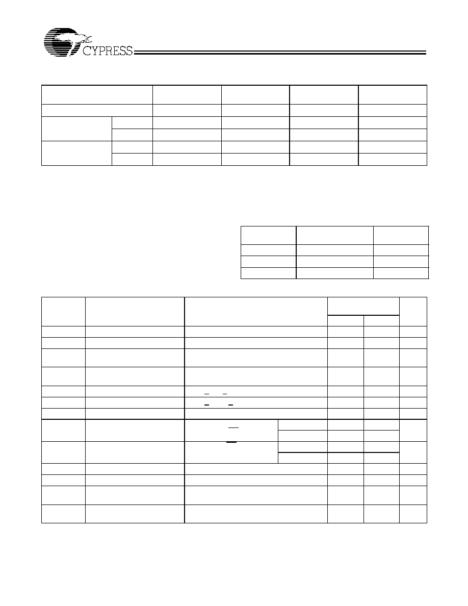
Selection Guide
7C271-30
7C274-30
7C271-35
7C274-35
7C271-45
7C274-45
7C271-55
7C274-55
Maximum Access Time (ns)
30
35
45
55
Maximum Operating
Current (mA)
Com'l
120
120
120
120
Military
130
130
130
Standby Current
(mA)
Com'l
30
30
30
30
Military
40
40
40
Operating Range
Range
Ambient
Temperature
V
CC
Commercial
0
°
C to +70
°
C
5V
±
10%
Industrial
[1]
-
40
°
C to +85
°
C
5V
±
10%
Military
[2]
-
55
°
C to +125
°
C
5V
±
10%
Electrical Characteristics
Over the Operating Range
[3]
7C271-30, 35, 45, 55
7C274-30, 35, 45, 55
Parameter
Description
Test Conditions
Min.
Max.
Unit
V
OH
Output HIGH Voltage
V
CC
= Min., I
OH
=
-
2.0 mA
2.4
V
V
OL
Output LOW Voltage
V
CC
= Min., I
OL
= 8.0 mA
[4]
0.4
V
V
IH
Input HIGH Level
Guaranteed Input Logical HIGH Voltage for All
Inputs
2.0
V
CC
V
V
IL
Input LOW Level
Guaranteed Input Logical LOW Voltage for All
Inputs
0.8
V
I
IX
Input Current
GND < V
IN
< V
CC
-
10
+10
µ
A
I
OZ
Output Leakage Current
GND < V
OUT
< V
CC
, Output Disabled
-
40
+40
µ
A
I
OS
Output Short Circuit Current
[5]
V
CC
= Max., V
OUT
= GND
-
20
-
90
mA
I
CC
Power Supply Current
V
CC
= Max., V
IN
= 2.0V,
I
OUT
= 0 mA, CE=V
IL
Commercial
120
mA
Military
130
I
SB
Standby Supply Current
V
CC
= Max., CE = V
IH
,
I
OUT
= 0 mA
Commercial
30
mA
Military
40
V
PP
Programming Supply Voltage
12
13
V
I
PP
Programming Supply Current
50
mA
V
IHP
Input HIGH Programming
Voltage
3.0
V
V
ILP
Input LOW Programming
Voltage
0.4
V
Note:
1.
Contact a Cypress representative for information on industrial temperature range specifications.
2.
T
A
is the "instant on" case temperature.
3.
See the last page of this specification for Group A subgroup testing information.
4.
6.0 mA military
5.
For test purposes, not more than one output at a time should be shorted. Short circuit test duration should not exceed 30 seconds.
CY7C271
CY7C274
Document #: 38-04008 Rev. **
Page 3 of 15
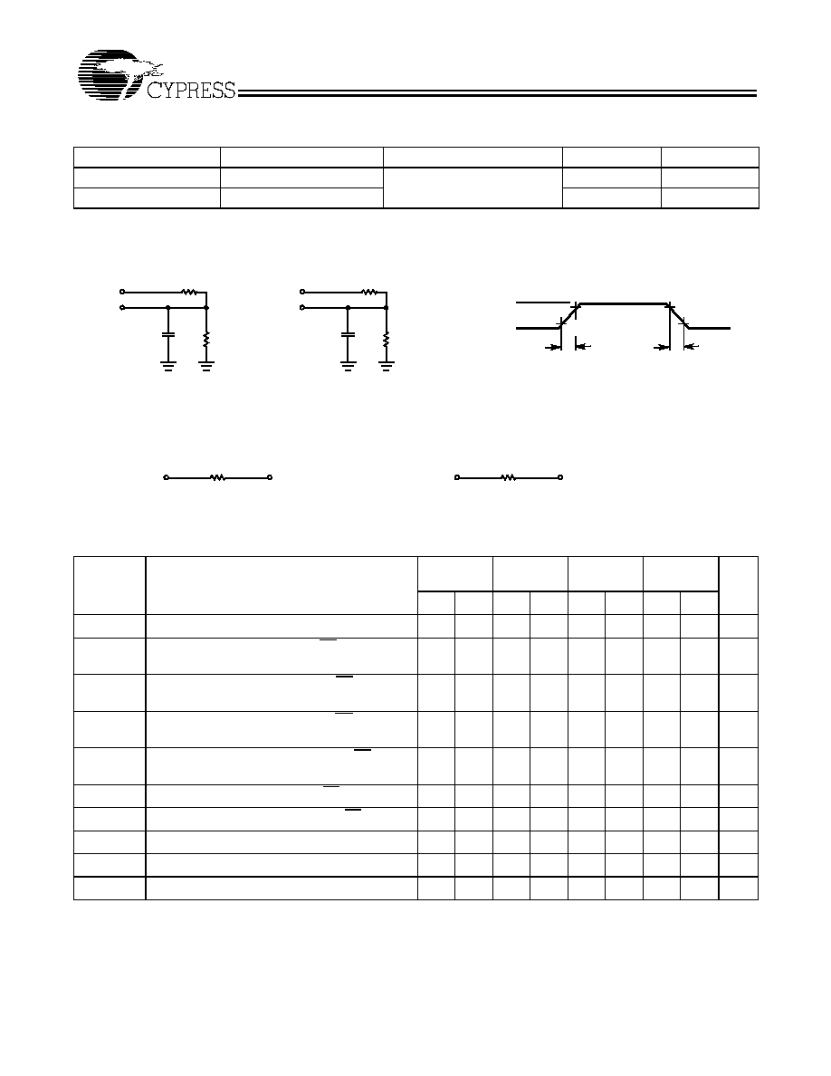
Capacitance
[6]
Parameter
Description
Test Conditions
Max.
Unit
C
IN
Input Capacitance
T
A
= 25
°
C, f = 1 MHz,
V
CC
= 5.0V
10
pF
C
OUT
Output Capacitance
10
pF
AC Test Loads and Waveforms
[6]
3.0V
5V
OUTPUT
R1 500
658
MIL
R2 333
(403
MIL)
30 pF
INCLUDING
JIG AND
SCOPE
GND
90%
10%
90%
10%
5 ns
5 ns
5V
OUTPUT
5 pF
INCLUDING
JIG AND
SCOPE
(a) Normal Load
(b) High Z Load
OUTPUT
2.00V COMMERCIAL
Equivalent to:
THÉ VENIN EQUIVALENT
200
ALL INPUT PULSES
OUTPUT
1.90V MILITARY
250
R1 500
658
MIL
R2 333
(403
MIL)
Switching Characteristics
Over the Operating Range
[3,6]
7C271-30
7C274-30
7C271-35
7C274-35
7C271-45
7C274-45
7C271-55
7C274-55
Parameter
Description
Min.
Max.
Min.
Max.
Min.
Max.
Min.
Max.
Unit
t
AA
Address to Output Valid
30
35
45
55
ns
t
HZCS
Chip Select Inactive to High Z (CS
1
and CS
2
,
7C271 Only)
20
25
30
30
ns
t
ACS
Chip Select Active to Output Valid (CS
1
and CS
2
,
7C271 Only)
20
25
30
30
ns
t
HZOE
Output Enable Inactive to High Z (OE, 7C274
Only)
20
20
25
25
ns
t
OE
Output Enable Active to Output Valid (OE, 7C274
Only)
20
20
25
25
ns
t
HZCE
Chip Enable Inactive to High Z (CE Only)
35
40
50
60
ns
t
ACE
Chip Enable Active to Output Valid (CE Only)
35
40
50
60
ns
t
PU
Chip Enable Active to Power Up
0
0
0
0
ns
t
PD
Chip Enable Inactive to Power Down
35
40
50
60
ns
t
OH
Output Hold from Address Change
0
0
0
0
ns
Note:
6.
See Introduction to CMOS PROMs for general information on testing.
CY7C271
CY7C274
Document #: 38-04008 Rev. **
Page 4 of 15
Erasure Characteristics
Wavelengths of light less than 4000 angstroms begin to erase
the 7C271 and 7C274 in the windowed package. For this rea-
son, an opaque label should be placed over the window if the
PROM is exposed to sunlight or fluorescent lighting for extend-
ed periods of time.
The recommended dose of ultraviolet light for erasure is a
wavelength of 2537 angstroms for a minimum dose (UV inten-
sity
×
exposure time) of 25 Wsec/cm
2
. For an ultraviolet lamp with a
12 mW/cm
2
power rating, the exposure time would be approximately
35 minutes. The 7C271 or 7C274 needs to be within 1 inch of the
lamp during erasure. Permanent damage may result if the PROM is
exposed to high-intensity UV light for an extended period of time.
7258 Wsec/cm
2
is the recommended maximum dosage.
Programming Modes
Programming support is available from Cypress as well as
from a number of third-party software vendors. For detailed
programming information, including a listing of software pack-
ages, please see the PROM Programming Information located
at the end of this section. Programming algorithms can be ob-
tained from any Cypress representative.
Switching Waveform
Note:
7.
CS
2
and CS
1
are used on the 7C271 only. OE is used on the 7C274 only.
t
OH
t
PU
t
PD
t
AA
(t
OE
)
t
ACS(E)
50%
50%
A
0
-
A
14
ADDRESS
V
CC
SUPPLY
CURRENT
CS
2
OE, CE, CS
1
O
0
- O
7
PREVIOUS DATA VALID
DATA VALID
POWER-DOWN CONTROLLED BY CE
(t
HZOE
)
t
HZCS(E)
HIGH Z
[7
Table 1. CY7C271 Mode Selection
Pin Function
[8]
Read or Output Disable
A
14
A
0
CE
CS
2
CS
1
O
7
O
0
Mode
Other
A
14
A
0
VFY
PGM
V
PP
D
7
D
0
Read
A
14
A
0
V
IL
V
IH
V
IL
O
7
O
0
Power Down
A
14
A
0
V
IH
X
X
High Z
Output Disable
A
14
A
0
X
V
IL
X
High Z
Output Disable
A
14
A
0
X
X
V
IH
High Z
Program
A
14
A
0
V
IHP
V
ILP
V
PP
D
7
D
0
Program Verify
A
14
A
0
V
ILP
V
IHP
/V
ILP
V
PP
O
7
O
0
Program Inhibit
A
14
A
0
V
IHP
V
IHP
V
PP
High Z
Blank Check
A
14
A
0
V
ILP
V
IHP
/V
ILP
V
PP
O
7
O
0
CY7C271
CY7C274
Document #: 38-04008 Rev. **
Page 5 of 15
Table 2. CY7C274 Mode Selection
Pin Function
[8]
Read or Output Disable
A
14
A
0
OE
CE
V
PP
O
7
O
0
Mode
Other
A
14
A
0
VFY
PGM
V
PP
D
7
D
0
Read
A
14
A
0
V
IL
V
IL
Note 9
O
7
O
0
Output Disable
A
14
A
0
V
IH
X
X
High Z
Power Down
A
14
A
0
X
V
IH
X
High Z
Program
A
14
A
0
V
IHP
V
ILP
V
PP
D
7
D
0
Program Verify
A
14
A
0
V
ILP
V
IHP
/V
ILP
V
PP
O
7
O
0
Program Inhibit
A
14
A
0
V
IHP
V
IHP
V
PP
High Z
Blank Check
A
14
A
0
V
ILP
V
IHP
/V
ILP
V
PP
O
7
O
0
Note:
8.
X can be V
IL
(V
ILP
) or V
IH
(V
IHP).
9.
V
PP
should be tied to V
CC
±
5% in read mode.
Figure 1. Programming Pinouts
1
2
3
4
5
6
7
8
9
10
11
12
16
17
18
19
20
24
23
22
21
13
14
25
28
27
26
A
9
A
8
A
7
A
6
A
5
A
4
A
3
A
2
A
1
A
0
D
0
D
1
D
2
GND
V
CC
A
10
A
11
A
12
A
13
A
14
V
PP
PGM
VFY
D
7
D
6
D
4
D
5
D
3
12
D
0
31
4
5
6
7
8
9
10
3 2 1
30
13
14151617
26
25
24
23
22
21
11
A
7
V
CC
A
6
A
5
A
4
A
3
A
2
A
1
A
0
PGM
A
14
NC
D
7
D
6
D
4
D
3
D
2
D
1
181920
27
28
29
32
NC
NC
D
5
15
V
PP
7C271
7C271
NC
GND
VFY
A
13
A
12
A
8
A
9
A
10
A
11
DIP
Top View
LCC
Top View
1
2
3
4
5
6
7
8
9
10
11
12
16
17
18
19
20
24
23
22
21
13
14
25
28
27
26
V
PP
A
12
A
7
A
6
A
5
A
4
A
3
A
2
A
1
A
0
D
0
D
1
D
2
GND
V
CC
A
14
A
13
A
8
A
9
A
11
A
10
PGM
VFY
D
7
D
6
D
4
D
5
D
3
12
D
0
31
4
5
6
7
8
9
10
3 2 1
30
13
14151617
26
25
24
23
22
21
11
A
7
V
CC
A
6
A
5
A
4
A
3
A
2
A
1
A
0
PGM
A
11
NC
D
7
D
6
D
4
D
3
D
2
D
1
181920
27
28
29
32
NC
NC
D
5
15
7C274
7C274
NC
GND
VFY
A
9
A
8
A
12
A
13
V
PP
A
14
A
10
DIP
Top View
LCC
Top View
CY7C271
CY7C274
Document #: 38-04008 Rev. **
Page 6 of 15
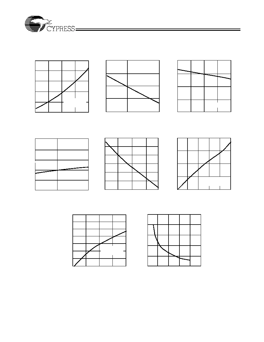
Typical DC and AC Characteristics
1.4
1.6
1.0
0.8
4.0
4.5
5.0
5.5
6.0
-
55
25
125
1.2
1.1
1.2
1.0
0.8
0.6
4.0
4.5
5.0
5.5
6.0
NORM
A
L
IZ
E
D
A
CCE
S
S
T
I
ME
SUPPLYVOLTAGE (V)
NORMALIZED SUPPLY CURRENT
vs. SUPPLY VOLTAGE
NORMALIZED SUPPLY CURRENT
vs. AMBIENTTEMPERATURE
AMBIENT TEMPERATURE (
°
C)
SUPPLYVOLTAGE (V)
NORMALIZED ACCESS TIME
vs. SUPPLY VOLTAGE
0.6
1.2
1.6
1.4
1.2
1.0
0.8
-
55
125
NORMA
L
I
Z
E
D
A
CCE
S
S
TI
M
E
AMBIENT TEMPERATURE (
°
C)
NORMALIZED ACCESS TIME
vs. TEMPERATURE
150
175
125
75
50
25
0.0
1.0
2.0
3.0
OUTP
UT S
I
N
K
C
URRE
NT
(mA
)
0
100
OUTPUT VOLTAGE (V)
OUTPUT SINK CURRENT
vs. OUTPUT VOLTAGE
1.0
0.9
0.8
NORM
A
L
IZ
E
D
I
CC
NORM
A
L
IZ
ED I
CC
V
CC
=5.0V
T
A
=25
°
C
T
A
=25
°
C
0.6
0.4
60
50
40
30
20
10
0
1.0
2.0
3.0
OUTP
UT
S
O
URCE
CURR
E
N
T (
m
A
)
OUTPUT VOLTAGE (V)
40
30
20
10
0
200
400
600
800
DEL
T
A t
(
n
s
)
AA
CAPACITANCE (pF)
TYPICAL ACCESS TIME CHANGE
vs. OUTPUT LOADING
4.0
1000
V
CC
=4.5V
T
A
=25
°
C
T
A
=25
°
C
f = f
MAX
25
0
OUTPUT SOURCE CURRENT
vs. VOLTAGE
4.0
C271-14
1.1
1.0
0.9
0.8
0.7
0
50
100
150
200
CYCLE PERIOD (ns)
NORMALIZED SUPPLY CURRENT
vs. CYCLE PERIOD
250
NORM
A
L
IZ
E
D
I
CC
0.6
0
CY7C271
CY7C274
Document #: 38-04008 Rev. **
Page 7 of 15
Ordering Information
[10]
Speed
(ns)
Ordering Code
Package
Name
Package Type
Operating
Range
30
CY7C271-30JC
J65
32-Lead Plastic Leaded Chip Carrier
Commercial
CY7C271-30PC
P21
28-Lead (300-Mil) Molded DIP
CY7C271-30WC
W22
28-Lead (300-Mil) Windowed CerDIP
35
CY7C271-35JC
J65
32-Lead Plastic Leaded Chip Carrier
Commercial
CY7C271-35PC
P21
28-Lead (300-Mil) Molded DIP
CY7C271-35WC
W22
28-Lead (300-Mil) Windowed CerDIP
CY7C271-35DMB
D22
28-Lead (300-Mil) CerDIP
Military
CY7C271-35KMB
K74
28-Lead Rectangular Cerpack
CY7C271-35LMB
L55
32-Pin Rectangular Leadless Chip Carrier
CY7C271-35QMB
Q55
32-Pin Windowed Rectangular Leadless Chip Carrier
CY7C271-35WMB
W22
28-Lead (300-Mil) Windowed CerDIP
45
CY7C271-45JC
J65
32-Lead Plastic Leaded Chip Carrier
Commercial
CY7C271-45PC
P21
28-Lead (300-Mil) Molded DIP
CY7C271-45WC
W22
28-Lead (300-Mil) Windowed CerDIP
CY7C271-45DMB
D22
28-Lead (300-Mil) CerDIP
Military
CY7C271-45KMB
K74
28-Lead Rectangular Cerpack
CY7C271-45LMB
L55
32-Pin Rectangular Leadless Chip Carrier
CY7C271-45QMB
Q55
32-Pin Windowed Rectangular Leadless Chip Carrier
CY7C271-45TMB
T74
28-Lead Windowed Cerpack
CY7C271-45WMB
W22
28-Lead (300-Mil) Windowed CerDIP
55
CY7C271-55JC
J65
32-Lead Plastic Leaded Chip Carrier
Commercial
CY7C271-55PC
P21
28-Lead (300-Mil) Molded DIP
CY7C271-55WC
W22
28-Lead (300-Mil) Windowed CerDIP
CY7C271-55DMB
D22
28-Lead (300-Mil) CerDIP
Military
CY7C271-55KMB
K74
28-Lead Rectangular Cerpack
CY7C271-55LMB
L55
32-Pin Rectangular Leadless Chip Carrier
CY7C271-55QMB
Q55
32-Pin Windowed Rectangular Leadless Chip Carrier
CY7C271-55TMB
T74
28-Lead Windowed Cerpack
CY7C271-55WMB
W22
28-Lead (300-Mil) Windowed CerDIP
Note:
10. Most of these products are available in industrial temperature range. Contact a Cypress representative for specifications and product availability.
CY7C271
CY7C274
Document #: 38-04008 Rev. **
Page 8 of 15
Ordering Information
[10]
(Continued)
Speed
(ns)
Ordering Code
Package
Name
Package Type
Operating
Range
30
CY7C274-30JC
J65
32-Lead Plastic Leaded Chip Carrier
Commercial
CY7C274-30PC
P15
28-Lead (600-Mil) Molded DIP
CY7C274-30WC
W16
28-Lead (600-Mil) Windowed CerDIP
35
CY7C274-35JC
J65
32-Lead Plastic Leaded Chip Carrier
Commercial
CY7C274-35PC
P15
28-Lead (600-Mil) Molded DIP
CY7C274-35WC
W16
28-Lead (600-Mil) Windowed CerDIP
CY7C274-35DMB
D16
28-Lead (600-Mil) CerDIP
Military
CY7C274-35KMB
K74
28-Lead Rectangular Cerpack
CY7C274-35LMB
L55
32-Pin Rectangular Leadless Chip Carrier
CY7C274-35QMB
Q55
32-Pin Windowed Rectangular Leadless Chip Carrier
CY7C274-35TMB
T74
28-Lead Windowed Cerpack
CY7C274-35WMB
W16
28-Lead (600-Mil) Windowed CerDIP
45
CY7C274-45JC
J65
32-Lead Plastic Leaded Chip Carrier
Commercial
CY7C274-45PC
P15
28-Lead (600-Mil) Molded DIP
CY7C274-45WC
W16
28-Lead (600-Mil) Windowed CerDIP
CY7C274-45DMB
D16
28-Lead (600-Mil) CerDIP
Military
CY7C274-45KMB
K74
28-Lead Rectangular Cerpack
CY7C274-45LMB
L55
32-Pin Rectangular Leadless Chip Carrier
CY7C274-45QMB
Q55
32-Pin Windowed Rectangular Leadless Chip Carrier
CY7C274-45TMB
T74
28-Lead Windowed Cerpack
CY7C274-45WMB
W16
28-Lead (600-Mil) Windowed CerDIP
55
CY7C274-55JC
J65
32-Lead Plastic Leaded Chip Carrier
Commercial
CY7C274-55PC
P15
28-Lead (600-Mil) Molded DIP
CY7C274-55WC
W16
28-Lead (600-Mil) Windowed CerDIP
CY7C274-55DMB
D16
28-Lead (600-Mil) CerDIP
Military
CY7C274-55KMB
K74
28-Lead Rectangular Cerpack
CY7C274-55LMB
L55
32-Pin Rectangular Leadless Chip Carrier
CY7C274-55QMB
Q55
32-Pin Windowed Rectangular Leadless Chip Carrier
CY7C274-55TMB
T74
28-Lead Windowed Cerpack
CY7C274-55WMB
W16
28-Lead (600-Mil) Windowed CerDIP
CY7C271
CY7C274
Document #: 38-04008 Rev. **
Page 9 of 15
MILITARY SPECIFICATIONS
Group A Subgroup Testing
DC Characteristics
Parameter
Subgroups
V
OH
1, 2, 3
V
OL
1, 2, 3
V
IH
1, 2, 3
V
IL
1, 2, 3
I
IX
1, 2, 3
I
OZ
1, 2, 3
I
CC
1, 2, 3
I
SB
1, 2, 3
Switching Characteristics
Parameter
Subgroups
t
AA
7, 8, 9, 10, 11
t
ACS
[11]
7, 8, 9, 10, 11
t
OE
[12]
7, 8, 9, 10, 11
t
ACE
7, 8, 9, 10, 11
Note:
11.
7C271 only (CS
1
and CS
2
).
12. 7C274 only.
SMD Cross Reference
SMD
Number
Suffix
Cypress
Number
5962-89817
01XX
CY7C271-55WMB
5962-89817
01YX
CY7C271-55TMB
5962-89817
01ZX
CY7C271-55QMB
5962-89817
02XX
CY7C271-45WMB
5962-89817
02YX
CY7C271-45TMB
5962-89817
02ZX
CY7C271-45QMB
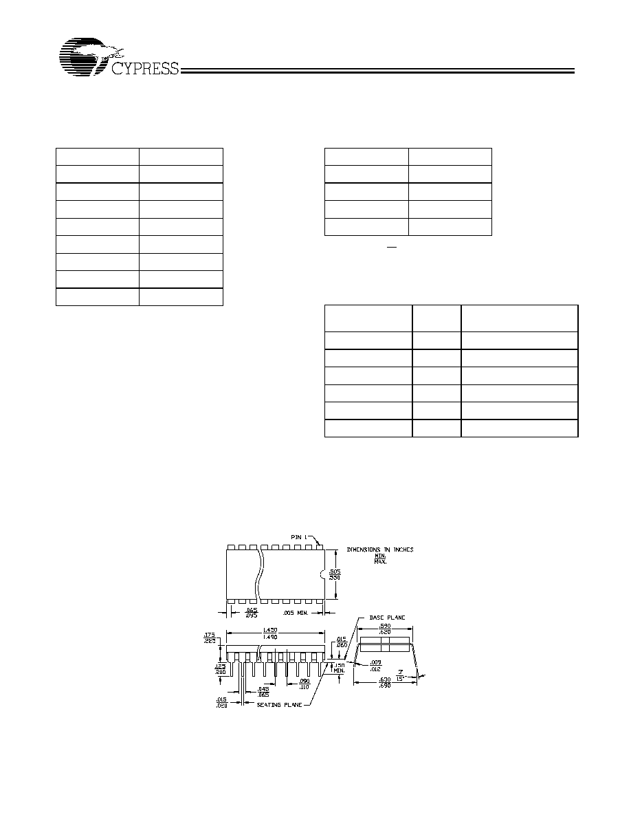
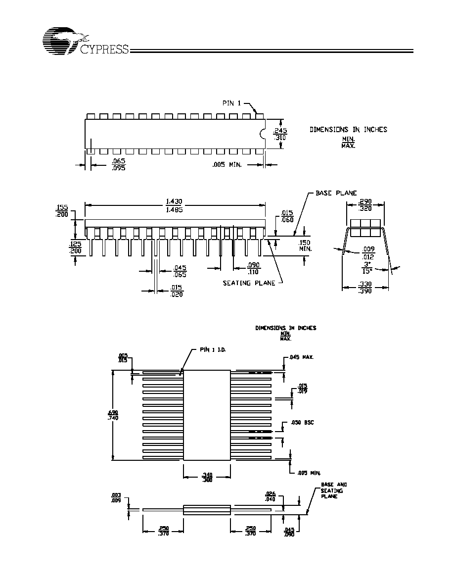
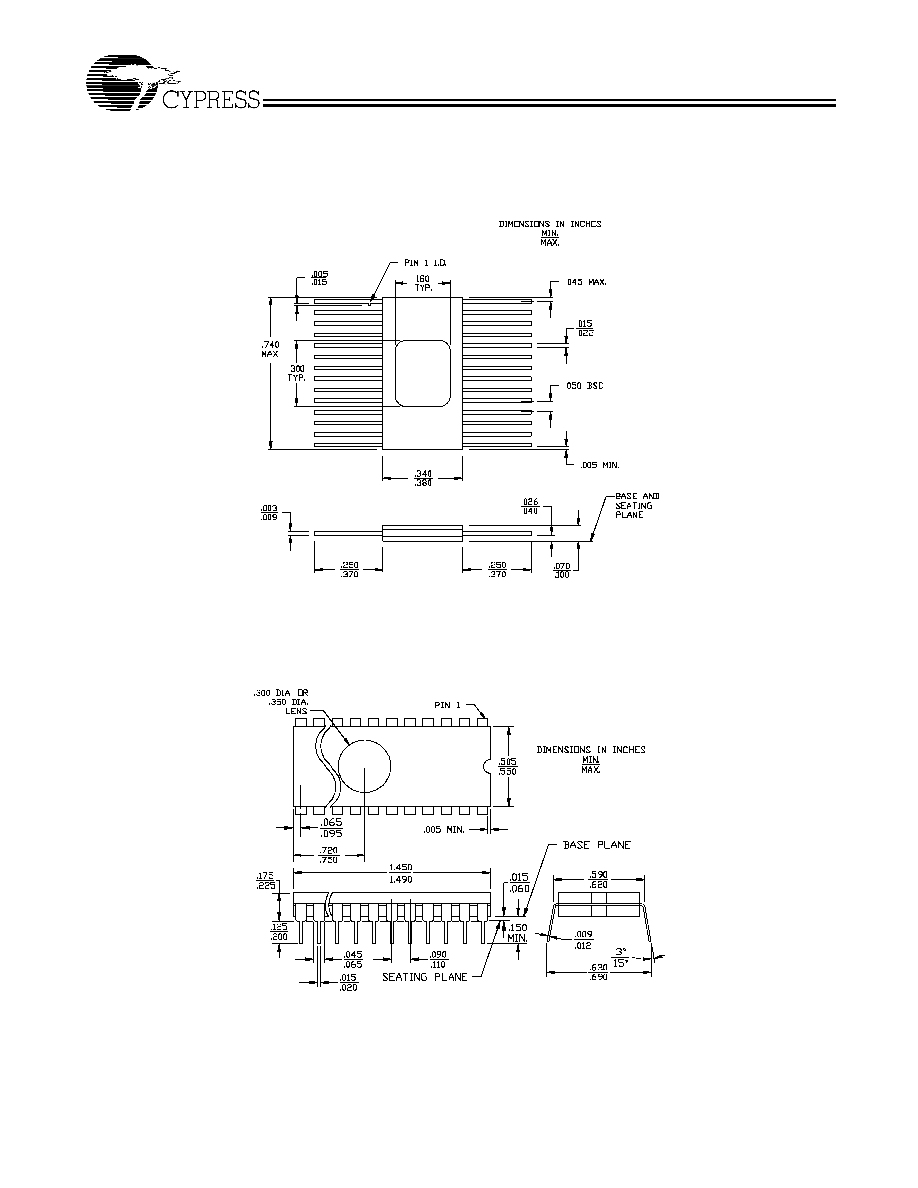
Package Diagrams
28-Lead (600-Mil) CerDIP D16
MIL-STD-1835 D-10 Config. A
51-80019
CY7C271
CY7C274
Document #: 38-04008 Rev. **
Page 10 of 15
Package Diagrams
(continued)
28-Lead (300-Mil) CerDIP D22
MIL-STD-1835 D-15 Config. A
51-80032
28-Lead Rectangular Cerpack K74
MIL-STD-1835 F-11 Config. A
51-80061
CY7C271
CY7C274
Document #: 38-04008 Rev. **
Page 11 of 15
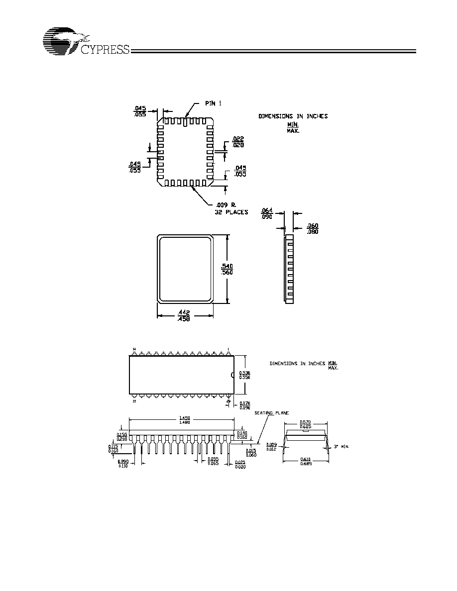
Package Diagrams
(continued)
32-Pin Rectangular Leadless Chip Carrier L55
MIL-STD-1835 C-12
51-80068
51-85017-A
28-Lead (600-Mil) Molded DIP P15
CY7C271
CY7C274
Document #: 38-04008 Rev. **
Page 12 of 15
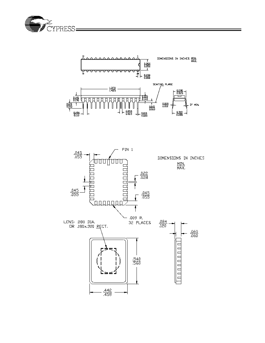
Package Diagrams
(continued)
51-85014-B
28-Lead (300-Mil) Molded DIP P21
MIL-STD-1835 C-12
51-80103-*A
32-Pin Windowed Rectangular Leadless Chip Carrier Q55
CY7C271
CY7C274
Document #: 38-04008 Rev. **
Page 13 of 15
Package Diagrams
(continued)
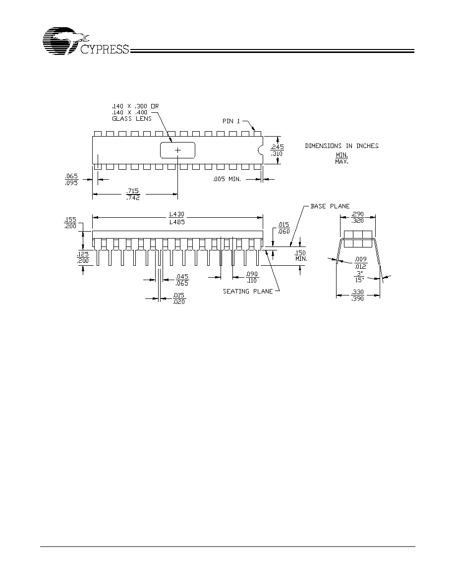
28-Lead Windowed Cerpack T74
28-Lead (600-Mil) Windowed CerDIP W16
MIL-STD-1835 D-10 Config. A
CY7C271
CY7C274
Document #: 38-04008 Rev. **
Page 14 of 15
© Cypress Semiconductor Corporation, 2002. The information contained herein is subject to change without notice. Cypress Semiconductor Corporation assumes no responsibility for the use
of any circuitry other than circuitry embodied in a Cypress Semiconductor product. Nor does it convey or imply any license under patent or other rights. Cypress Semiconductor does not authorize
its products for use as critical components in life-support systems where a malfunction or failure may reasonably be expected to result in significant injury to the user. The inclusion of Cypress
Semiconductor products in life-support systems application implies that the manufacturer assumes all risk of such use and in doing so indemnifies Cypress Semiconductor against all charges.
Package Diagrams
(continued)
28-Lead (300-Mil) Windowed CerDIP W22
MIL-STD-1835 D-15 Config. A
51-80087

CY7C271
CY7C274
Document #: 38-04008 Rev. **
Page 15 of 15
Document Title: CY7C271 CY7C274 32K x 8 Power Switched and Reprogrammable PROM
Document Number: 38-04008
REV.
ECN NO.
Issue
Date
Orig. of
Change
Description of Change
**
113864
3/8/02
DSG
Change from Spec number: 38-00068 to 38-04008
Document Outline