32K x 8 Reprogrammable Registered PROM
CY7C277
Cypress Semiconductor Corporation
·
3901 North First Street
·
San Jose
·
CA 95134
·
408-943-2600
Document #: 38-04006 Rev. **
Revised March 4, 2002
77
Features
· Windowed for reprogrammability
· CMOS for optimum speed/power
· High speed
-- 30-ns address set-up
-- 15-ns clock to output
· Low power
-- 60 mW (commercial)
-- 715 mW (military)
· Programmable address latch enable input
· Programmable synchronous or asynchronous output
enable
· On-chip edge-triggered output registers
· EPROM technology, 100% programmable
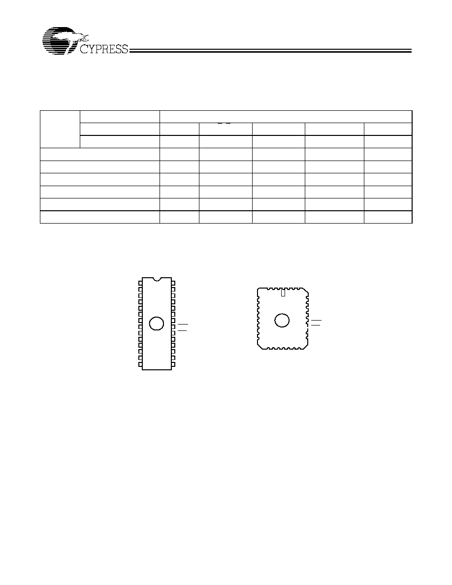
· Slim 300-mil, 28-pin plastic or hermetic DIP
· 5V
±
10% V
CC
, commercial and military
· TTL-compatible I/O
· Direct replacement for bipolar PROMs
· Capable of withstanding greater than 2001V static dis-
charge
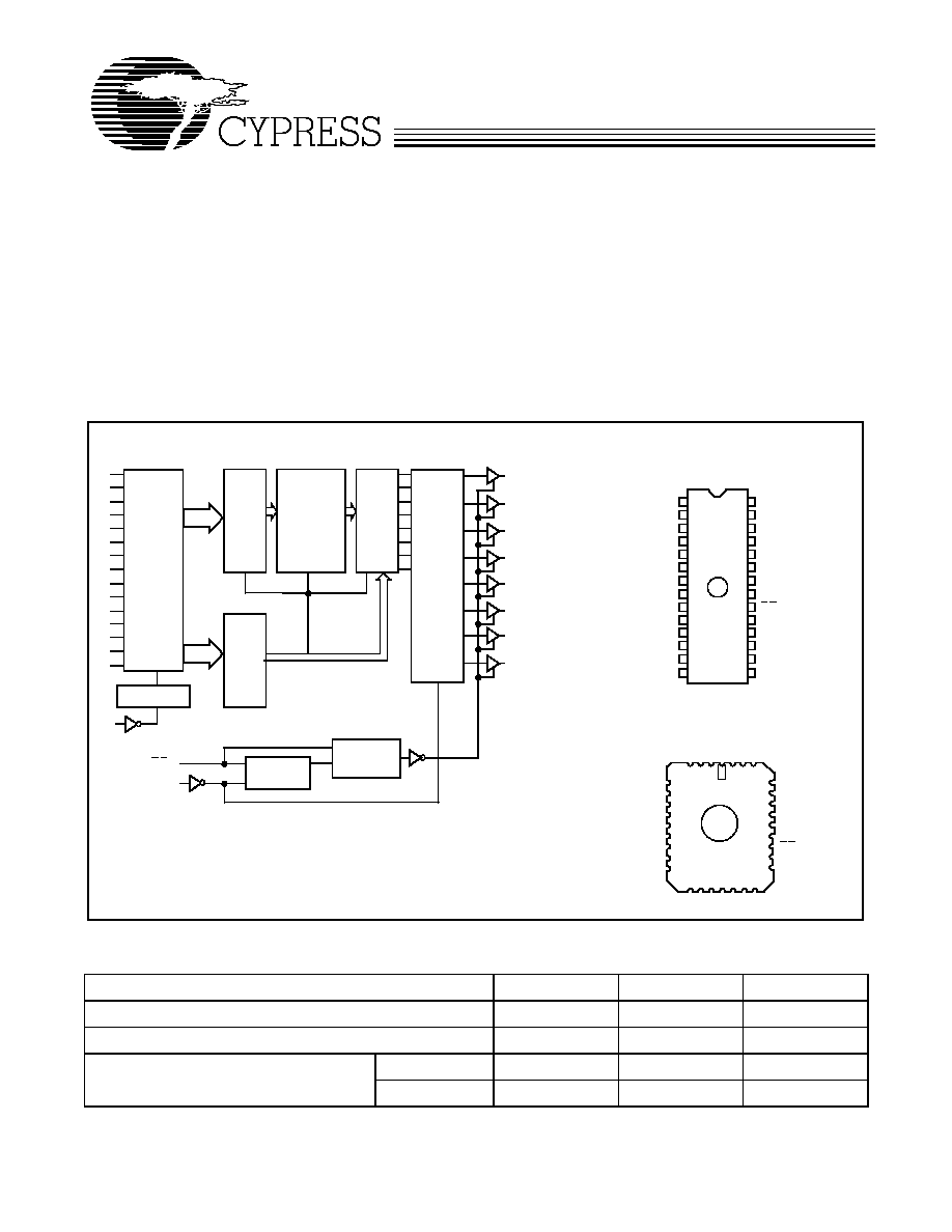
PROGRAMMABLE
MULTIPLEXER
PROGRAMMABLE
CP/ALE OPTIONS
Logic Block Diagram
Pin Configurations
1
2
3
4
5
6
7
8
9
10
11
12
16
17
18
19
20
24
23
22
21
13
14
25
28
27
26
A
9
A
8
A
7
A
6
A
5
A
4
A
3
A
2
A
1
A
0
O
0
O
1
O
2
GND
V
CC
A
10
A
11
A
12
A
13
A
14
ALE
CP
E/E
S
O
7
O
6
O
4
O
5
O
3
12
O
0
31
4
5
6
7
8
9
10
3 2 1
30
13
14151617
26
25
24
23
22
21
11
A
7
V CC
A
6
A
5
A
4
A
3
A
2
A
1
A
0
A
13
A
14
NC
CP
O
7
O
6
O
5
GND
LCC/PLCC (Opaque Only)
A
12
ALE
A
8
O
4
O
2
O
1
181920
27
28
29
32
15
O
3
A
9
A
10
A
11
E/E
S
NC
NC
A
14
A
13
A
12
A
11
A
10
A
9
A
8
8-BIT
1 OF 128
MUX
A
7
A
6
A
5
A
4
A
3
A
2
A
1
A
0
E/E
S
CP
15-BIT
ADDRESS
TRANSPARENT/
LATCH
256 x 1024
PROGRAMMABLE
ARRAY
8-BIT
EDGE-
TRIGGERED
REGISTER
ROW
DECODER
1 OF 256
ALE
COLUMN
DECODER
1 OF 32
ALE
CP
D
C
Q
NC
Top View
DIP/Flatpack
Top View
Y
ADDRESS
X
ADDRESS
O
7
O
6
O
5
O
4
O
3
O
2
O
1
O
0
Selection Guide
7C277-30
7C277-40
7C277-50
Minimum Address Set-Up Time (ns)
30
40
50
Maximum Clock to Output (ns)
15
20
25
Maximum Operating
Current (mA)
Com'l
120
120
120
Mil
130
130
CY7C277
Document #: 38-04006 Rev. **
Page 2 of 13
Functional Description
The CY7C277 is a high-performance 32K word by 8-bit CMOS
PROMs. It is packaged in the slim 28-pin 300-mil package.
The ceramic package may be equipped with an erasure win-
dow; when exposed to UV light, the PROM is erased and can
then be reprogrammed. The memory cells utilize proven
EPROM floating-gate technology and byte-wide algorithms.
The CY7C277 offers the advantages of low power, superior
performance, and high programming yield. The EPROM cell
requires only 12.5V for the supervoltage and low current re-
quirements allow for gang programming. The EPROM cells
allow for each memory location to be 100% tested, as each
location is written into, erased, and repeatedly exercised prior
to encapsulation. Each PROM is also tested for AC perfor-
mance to guarantee that the product will meet DC and AC
specification limits after customer programming.
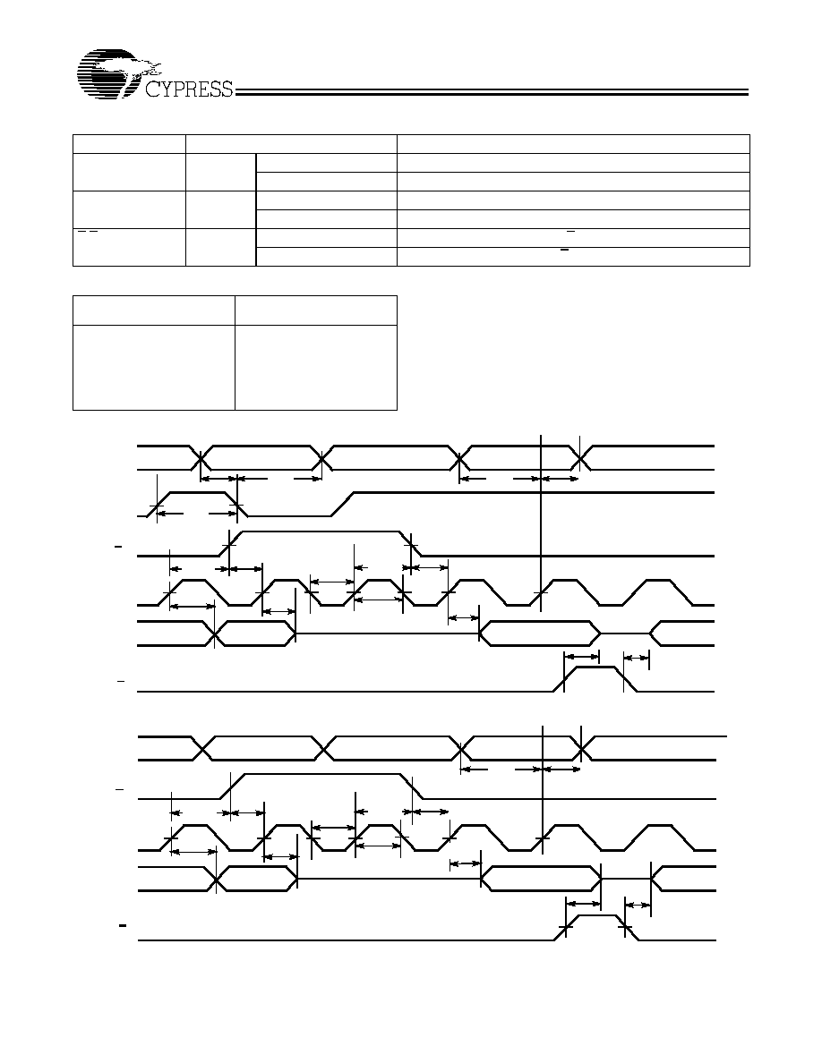
On the 7C277, the outputs are pipelined through a mas-
ter-slave register. On the rising edge of CP, data is loaded into
the 8-bit edge triggered output register. The E/E
S
input pro-
vides a programmable bit to select between asynchronous
and synchronous operation. The default condition is asynchro-
nous. When the asynchronous mode is selected, the E/E
S
pin
operates as an asynchronous output enable. If the synchro-
nous mode is selected, the E/E
S
pin is sampled on the rising
edge of CP to enable and disable the outputs. The 7C277 also
provides a programmable bit to enable the Address Latch in-
put. If this bit is not programmed, the device will ignore the ALE
pin and the address will enter the device asynchronously. If the
ALE function is selected, the address enters the PROM while
the ALE pin is active, and is captured when ALE is deasserted.
The user may define the polarity of the ALE signal, with the
default being active HIGH.
Maximum Ratings
(Above which the useful life may be impaired. For user guide-
lines, not tested.)
Storage Temperature
....................................-
65
°
C to +150
°
C
Ambient Temperature with
Power Applied
.................................................-
55
°
C to +125
°
C
Supply Voltage to Ground Potential
.................-
0.5V to +7.0V
(Pin 24 to Pin 12)
DC Voltage Applied to Outputs
in High Z State
.....................................................-
0.5V to +7.0V
DC Input Voltage
.................................................-
3.0V to +7.0V
DC Program Voltage (Pins 7, 18, 20) ........................... 13.0V
UV Erasure ................................................... 7258 Wsec/cm
2
Static Discharge Voltage ........................................... >2001V
(per MIL-STD-883, Method 3015)
Latch-Up Current ..................................................... >200 mA
Operating Range
Range
Ambient Temperature
V
CC
Commercial
0
°
C to +70
°
C
5V
±
10%
Industrial
[1]
-
40
°
C to +85
°
C
5V
±
10%
Military
[2]
-
55
°
C to +125
°
C
5V
±
10%
Electrical Characteristics
Over the Operating Range
[3, 4]
Parameter
7C277-30
7C277-40, 50
Description
Test Conditions
Min.
Max.
Min.
Max.
Unit
V
OH
Output HIGH Voltage
V
CC
= Min., I
OH
=
-
2.0 mA
2.4
2.4
V
V
OL
Output LOW Voltage
V
CC
= Min., I
OL
= 8.0 mA
0.4
0.4
V
V
IH
Input HIGH Level
Guaranteed Input Logical HIGH
Voltage for All Inputs
2.0
V
CC
2.0
V
CC
V
V
IL
Input LOW Level
Guaranteed Input Logical LOW
Voltage for All Inputs
0.8
0.8
V
I
IX
Input Leakage Current
GND < V
IN
< V
CC
-
10
+
10
-
10
+10
µ
A
V
CD
Input Clamp Diode Voltage
Note 4
I
OZ
Output Leakage Current
0 < V
OUT
< V
CC
, Output Disabled
[5]
-
40
+40
-
40
+40
µ
A
I
OS
Output Short Circuit Current
V
CC
= Max., V
OUT
= 0.0V
[6]
-
20
-
90
-
20
-
90
mA
I
CC
Power Supply Current
V
CC
= Max., CS > V
IH
I
OUT
= 0 mA
Commercial
120
120
mA
Military
130
V
PP
Programming Supply Voltage
12
13
12
13
V
I
PP
Programming Supply Current
50
50
mA
V
IHP
Input HIGH Programming Voltage
3.0
3.0
V
V
ILP
Input LOW Programming Voltage
0.4
0.4
V
Notes:
1.
Contact a Cypress representative for industrial temperature range specifications.
2.
T
A
is the "instant on" case temperature.
3.
See the last page of this specification for Group A subgroup testing information.
4.
See "Introduction to CMOS PROMs" in this Book for general information on testing.
5.
For devices using the synchronous enable, the device must be clocked after applying these voltages to perform this measurement.
6.
For test purposes, not more than one output at a time should be shorted. Short circuit test duration should not exceed 30 seconds.
CY7C277
Document #: 38-04006 Rev. **
Page 3 of 13
Capacitance
[4]
Parameter
Description
Test Conditions
Max.
Unit
C
IN
Input Capacitance
T
A
= 25
°
C, f = 1 MHz,
V
CC
= 5.0V
10
pF
C
OUT
Output Capacitance
10
pF
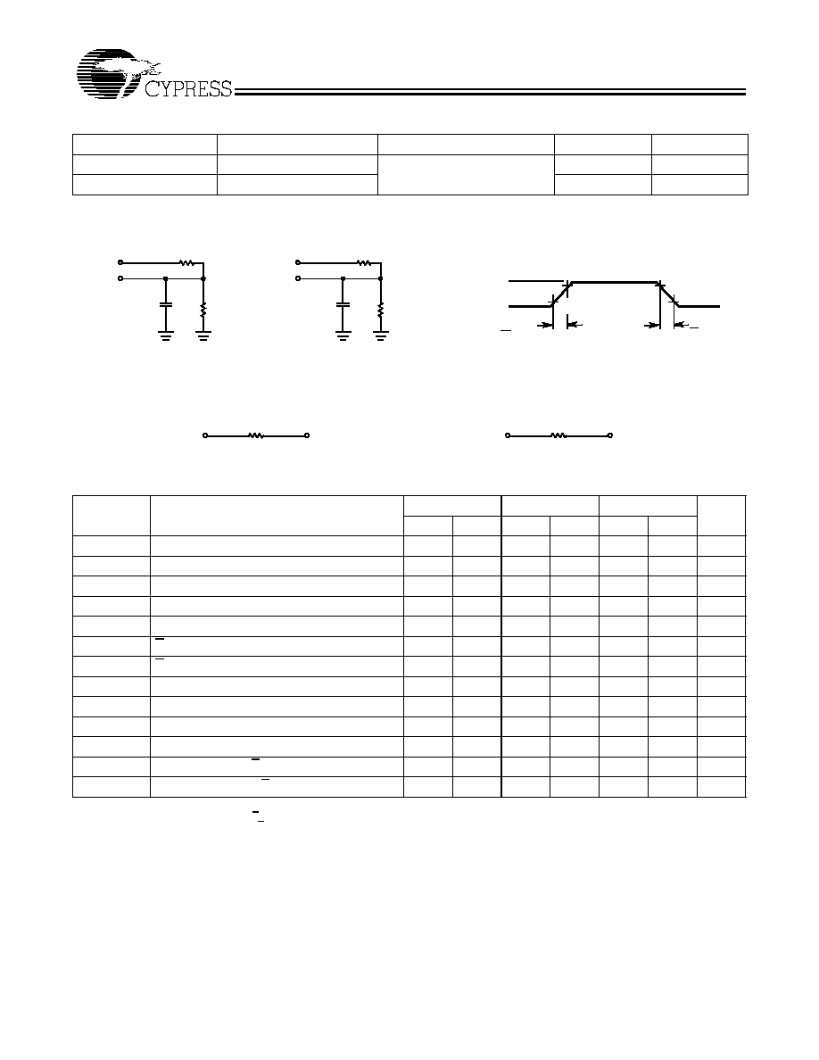
AC Test Loads and Waveforms
[4]
3.0V
5V
OUTPUT
R1 500
R2
333
30 pF
INCLUDING
JIG AND
SCOPE
GND
90%
10%
90%
10%
< 5 ns
< 5 ns
5V
OUTPUT
R1 500
R2
333
5 pF
INCLUDING
JIG AND
SCOPE
(a) Normal Load
(b) High Z Load
OUTPUT
2.0V
Equivalent to:
THÉ VENIN EQUIVALENT
ALL INPUT PULSES
(658
MIL)
(403
MIL)
(403
MIL)
OUTPUT
1.9V
Commercial
Military
(658
MIL)
200
250
CY7C277 Switching Characteristics
Over the Operating Range
[3, 4]
7C277-30
7C277-40
7C277-50
Parameter
Description
Min.
Max.
Min.
Max.
Min.
Max.
Unit
t
AL
Address Set-Up to ALE Inactive
5
10
10
ns
t
LA
Address Hold from ALE Inactive
10
10
15
ns
t
LL
ALE Pulse Width
10
10
15
ns
t
SA
Address Set-Up to Clock HIGH
30
40
50
ns
t
HA
Address Hold from Clock HIGH
0
0
0
ns
t
SES
E
S
Set-Up to Clock HIGH
12
15
15
ns
t
HES
E
S
Hold from Clock HIGH
5
10
10
ns
t
CO
Clock HIGH to Output Valid
15
20
25
ns
t
PWC
Clock Pulse Width
15
20
20
ns
t
LZC
[7]
Output Valid from Clock HIGH
15
20
30
ns
t
HZC
Output High Z from Clock HIGH
15
20
30
ns
t
LZE
[8]
Output Valid from E LOW
15
20
30
ns
t
HZE
[8]
Output High Z from E HIGH
15
20
30
ns
Notes:
7.
Applies only when the synchronous (E
S
) function is used.
8.
Applies only when the asynchronous (E) function is used.