2K x 8 Reprogrammable PROM
CY7C291A
CY7C292A/CY7C293A
Cypress Semiconductor Corporation
∑
3901 North First Street
∑
San Jose
∑
CA 95134
∑
408-943-2600
March 1986 ≠ Revised May 1993
92A
Features
∑
Windowed for reprogrammability
∑
CMOS for optimum speed/power
∑
High speed
-- 20 ns (commercial)
-- 25 ns (military)
∑
Low power
-- 660 mW (commercial and military)
∑
Low standby power
-- 220 mW (commercial and military)
∑
EPROM technology 100% programmable
∑
Slim 300-mil or standard 600-mil packaging available
∑
5V
±
10% V
CC
, commercial and military
∑
TTL-compatible I/O
∑
Direct replacement for bipolar PROMs
∑
Capable of withstanding >2001V static discharge
Functional Description
The CY7C291A, CY7C292A, and CY7C293A are high-perfor-
mance 2K-word by 8-bit CMOS PROMs. They are functionally
identical, but are packaged in 300-mil (7C291A, 7C293A) and
600-mil wide plastic and hermetic DIP packages (7C292A).
The CY7C293A has an automatic power down feature which
reduces the power consumption by over 70% when deselect-
ed. The 300-mil ceramic package may be equipped with an
erasure window; when exposed to UV light the PROM is
erased and can then be reprogrammed. The memory cells uti-
lize proven EPROM floating-gate technology and byte-wide in-
telligent programming algorithms.
The CY7C291A, CY7C292A, and CY7C293A are plug-in re-
placements for bipolar devices and offer the advantages of
lower power, reprogrammability, superior performance and
programming yield. The EPROM cell requires only 12.5V for
the supervoltage and low current requirements allow for gang
programming. The EPROM cells allow for each memory loca-
tion to be tested 100%, as each location is written into, erased,
and repeatedly exercised prior to encapsulation. Each PROM
is also tested for AC performance to guarantee that after cus-
tomer programming the product will meet DC and AC specifi-
cation limits.
A read is accomplished by placing an active LOW signal on
CS
1
, and active HIGH signals on CS
2
and CS
3
. The contents
of the memory location addressed by the address line (A
0
-
A
10
) will become available on the output lines (O
0
-
O
7
).
Logic Block Diagram
Pin Configurations
C291A-1
C291A-2
C291A-3
O
7
O
6
O
5
O
4
O
3
O
2
O
1
O
0
PROGRAM-
MABLE
ARRAY
MULTI-
PLEXER
GND
1
2
3
4
5
6
7
8
9
10
11
14
15
16
20
19
18
17
21
24
23
22
A
6
A
5
A
4
A
3
A
2
A
1
A
0
O
0
A
7
O
3
V
CC
A
8
A
9
A
10
O
7
O
6
O
5
O
4
CS
1
O
2
12
13
O
1
CS
3
CS
2
28
4
5
6
7
8
9
10
3 2 1
27
1314151617
26
25
24
23
22
21
20
11
12
19
A
5
V CC
GND
A
6
A
7
O
3
O
1
O
0
18
O
4
O
5
NC
A
0
A
4
A
3
A
10
NC
A
8
A
9
NC
NC
CS
1
CS
2
O
7
O
6
A
2
A
1
CS
3
O
2
CS
1
CS
2
CS
3
POWER
DOWN
7C293A
Window available on
7C291A and 7C293A
only.
DIP
LCC/PLCC (Opaque Only)
Top View
Top View
ADDRESS
DECODER
A
0
A
1
A
2
A
3
A
4
A
5
A
6
A
8
A
9
A
10
A
7
COLUMN
ADDRESS
ROW
ADDRESS
7C291A
7C292A
7C293A
7C291A
7C293A
CY7C291A
CY7C292A/CY7C293A
2
Maximum Ratings
(Above which the useful life may be impaired. For user guide-
lines, not tested.)
Storage Temperature
......................................-
65
∞
C to+150
∞
C
Ambient Temperature with
Power Applied
...................................................-
55
∞
C to+125
∞
C
Supply Voltage to Ground Potential
...................-
0.5V to+7.0V
DC Voltage Applied to Outputs
in High Z State
......................................................-
0.5V to+7.0V
DC Input Voltage
.................................................-
3.0V to +7.0V
DC Program Voltage .....................................................13.0V
UV Exposure.................................................7258 Wsec/cm
2
Static Discharge Voltage ............................................>2001V
(per MIL-STD-883, Method 3015)
Latch-Up Current ..................................................... >200 mA
Selection Guide
7C291A-20
7C292A-20
7C293A-20
7C291A-25
7C292A-25
7C293A-25
7C291AL-25
7C292AL-25
7C293AL-25
7C291A-35
7C292A-35
7C293A-35
7C291AL-35
7C292AL-35
7C293AL-35
7C291A-50
7C292A-50
7C293A-50
7C291AL-50
7C292AL-50
7C293AL-50
Maximum Access Time (ns)
20
25
35
50
Maximum Operating
Current (mA)
Standard
Commercial
120
90
90
90
Military
120
90
90
L
Commercial
60
60
60
Standby Current (mA)
7C293A Only
Commercial
40
30
30
30
Military
40
40
40
Operating Range
Range
Ambient
Temperature
V
CC
Commercial
0
∞
C to + 70
∞
C
5V
±
10%
Industrial
[1]
-
40
∞
C to + 85
∞
C
5V
±
10%
Military
[2]
-
55
∞
C to + 125
∞
C
5V
±
10%
Notes:
1.
Contact a Cypress representative for industrial temperature range spec-
ifications.
2.
T
A
is the "instant on" case temperature.
CY7C291A
CY7C292A/CY7C293A
3
Electrical Characteristics
Over the Operating Range
[3,4]
7C291A-20
7C292A-20
7C293A-20
7C291A-25
7C292A-25
7C293A-25
7C291AL-25
7C292AL-25
7C293AL-25
Parameter
Description
Test Conditions
Min.
Max.
Min.
Max.
Min.
Max.
Unit
V
OH
Output HIGH Voltage
V
CC
= Min., I
OH
=
-
4.0 mA
2.4
2.4
2.4
V
V
OL
Output LOW Voltage
V
CC
= Min., I
OL
= 16.0 mA
0.4
0.4
0.4
V
V
IH
Input HIGH Voltage
Guaranteed Input Logical
HIGH Voltage for All Inputs
2.0
V
CC
2.0
V
CC
2.0
V
CC
V
V
IL
Input LOW Voltage
Guaranteed Input Logical
LOW Voltage for All Inputs
0.8
0.8
0.8
V
I
IX
Input Load Current
GND < V
IN
< V
CC
-
10
+10
-
10
+10
-
10
+10
µ
A
V
CD
Input Diode Clamp Voltage
Note 4
I
OZ
Output Leakage Current
GND < V
OUT
< V
CC
,
Output Disabled
-
10
+10
-
10
+10
-
10
+10
µ
A
I
OS
Output Short Circuit
Current
[5]
V
CC
= Max., V
OUT
= GND
-
20
-
90
-
20
-
90
-
20
-
90
mA
I
CC
V
CC
Operating Supply
Current
V
CC
= Max.,
I
OUT
= 0 mA
Com'l
120
90
60
mA
Mil
120
I
SB
Standby Supply Current
(7C293A Only)
V
CC
= Max.,
CS
1
= V
IH
Com'l
40
30
30
mA
Mil
40
V
PP
Programming Supply Voltage
12
13
12
13
12
13
V
I
PP
Programming Supply Current
50
50
50
mA
V
IHP
Input HIGH Programming
Voltage
3.0
3.0
3.0
V
V
ILP
Input LOW Programming
Voltage
0.4
0.4
0.4
V
Notes:
3.
See the last page of this specification for Group A subgroup testing information.
4.
See the "Introduction to CMOS PROMs" section of the Cypress Data Book for general information on testing.
5.
For test purposes, not more than one output at a time should be shorted. Short circuit test duration should not exceed 30 seconds.
CY7C291A
CY7C292A/CY7C293A
4
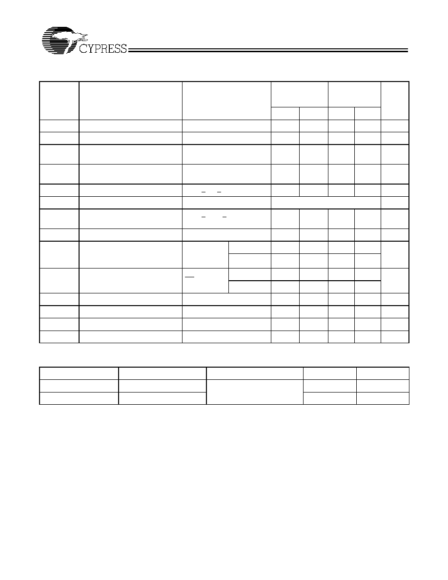
Electrical Characteristics
Over the Operating Range
[3,4]
(continued)
7C291AL-35, 50
7C292AL-35, 50
7C293AL-35, 50
7C291A-35, 50
7C292A-35, 50
7C293A-35, 50
Parameter
Description
Test Conditions
Min.
Max.
Min.
Max.
Unit
V
OH
Output HIGH Voltage
V
CC
= Min., I
OH
=
-
4.0 mA
2.4
2.4
V
V
OL
Output LOW Voltage
V
CC
= Min., I
OL
= 16.0 mA
0.4
0.4
V
V
IH
Input HIGH Voltage
Guaranteed Input Logical
HIGH Voltage for All Inputs
2.0
2.0
V
V
IL
Input LOW Voltage
Guaranteed Input Logical
LOW Voltage for All Inputs
0.8
0.8
V
I
IX
Input Load Current
GND < V
IN
< V
CC
-
10
+10
-
10
+10
µ
A
V
CD
Input Diode Clamp Voltage
Note 4
I
OZ
Output Leakage Current
GND < V
OUT
< V
CC
,
Output Disabled
-
10
+10
-
10
+10
µ
A
I
OS
Output Short Circuit Current
[5]
V
CC
= Max., V
OUT
= GND
-
20
-
90
-
20
-
90
mA
I
CC
V
CC
Operating Supply Current
V
CC
= Max.,
V
IN
= 2.0V
I
OUT
=0 mA
Commercial
60
90
mA
Military
90
I
SB
Standby Supply Current
(7C293A Only)
V
CC
= Max.,
CS
1
=V
IH
Commercial
30
30
mA
Military
40
V
PP
Programming Supply Voltage
12
13
12
13
V
I
PP
Programming Supply Current
50
50
mA
V
IHP
Input HIGH Programming Voltage
3.0
3.0
V
V
ILP
Input LOW Programming Voltage
0.4
0.4
V
Capacitance
[4]
Parameter
Description
Test Conditions
Max.
Unit
C
IN
Input Capacitance
T
A
= 25
∞
C, f = 1 MHz,
V
CC
= 5.0V
10
pF
C
OUT
Output Capacitance
10
pF
CY7C291A
CY7C292A/CY7C293A
5
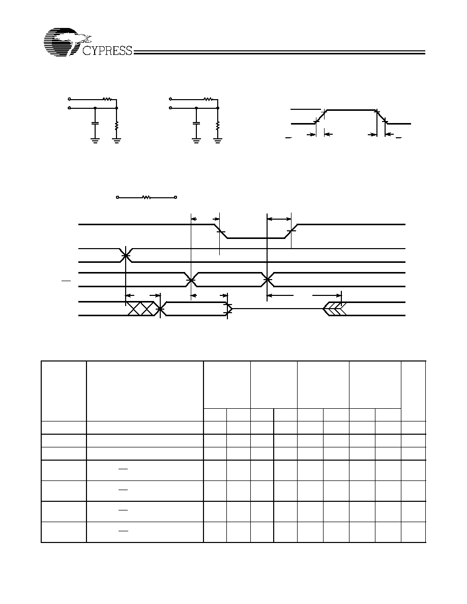
AC Test Loads and Waveforms
[4]
t
PU
t
AA
t
HZCS
t
ACS
50%
50%
t
PD
3.0V
5V
OUTPUT
R1250
R2
167
30pF
INCLUDING
JIG AND
SCOPE
GND
90%
10%
90%
10%
< 5 ns
< 5 ns
5V
OUTPUT
5 pF
INCLUDING
JIG AND
SCOPE
(a) Normal Load
(b) High Z Load
OUTPUT
2.0V
Equivalent to:
TH…
VENIN EQUIVALENT
C291A-4
C291A-5
100
C291A-6
R1250
R2
167
ALL INPUT PULSES
CS
2
-
CS
3
CS
1
V
CC
SUPPLY
CURRENT
A
0
-
A
10
ADDRESS
O
0
- O
7
C291A-7
Switching Characteristics
Over the Operating Range
[3, 4]
7C291A-20
7C292A-20
7C293A-20
7C291A-25
7C292A-25
7C293A-25
7C291AL-25
7C292AL-25
7C293AL-25
7C291A-35
7C292A-35
7C293A-35
7C291AL-35
7C292AL-35
7C293AL-35
7C291A-50
7C292A-50
7C293A-50
7C291AL-50
7C292AL-50
7C293AL-50
Parameter
Description
Min.
Max.
Min.
Max.
Min.
Max.
Min.
Max.
Unit
t
AA
Address to Output Valid
20
25
35
50
ns
t
HZCS1
Chip Select Inactive to High Z
15
15
20
20
ns
t
ACS1
Chip Select Active to Output Valid
15
15
20
20
ns
t
HZCS2
Chip Select Inactive to High Z
(7C293A CS
1
Only)
[6]
22
27
35
45
ns
t
ACS2
Chip Select Active to Output Valid
(7C293A CS
1
Only)
[6]
22
27
35
45
ns
t
PU
Chip Select Active to Power-Up
(7C293A CS
1
Only)
0
0
0
0
ns
t
PD
Chip Select Inactive to Power-Down
(7C293A CS
1
Only)
22
27
35
45
ns