128-Macrocell MAX
Æ
EPLD
CY7C342B
USE ULTRA37000
TM
FOR
ALL NEW DESIGNS
Cypress Semiconductor Corporation
∑
3901 North First Street
∑
San Jose
,
CA 95134
∑
408-943-2600
Document #: 38-03014 Rev. *B
Revised April 22, 2004
Features
∑ 128 macrocells in eight logic array blocks (LABs)
∑ Eight dedicated inputs, 52 bidirectional I/O pins
∑ Programmable interconnect array
∑ Advanced 0.65-micron CMOS technology to increase
performance
∑ Available in 68-pin HLCC, PLCC, and PGA packages
Functional Description
The CY7C342B is an Erasable Programmable Logic Device
(EPLD) in which CMOS EPROM cells are used to configure
logic functions within the device. The MAX
Æ
architecture is
100% user-configurable, allowing the device to accommodate
a variety of independent logic functions.
The 128 macrocells in the CY7C342B are divided into eight
LABs, 16 per LAB. There are 256 expander product terms, 32
per LAB, to be used and shared by the macrocells within each
LAB.
Each LAB is interconnected with a programmable interconnect
array, allowing all signals to be routed throughout the chip.
The speed and density of the CY7C342B allows it to be used in a
wide range of applications, from replacement of large amounts of
7400-series TTL logic, to complex controllers and multifunction
chips. With greater than 25 times the functionality of 20-pin PLDs,
the CY7C342B allows the replacement of over 50 TTL devices.
By replacing large amounts of logic, the CY7C342B reduces board
space, part count, and increases system reliability.
MACROCELL 101
MACROCELL 100
MACROCELL 99
MACROCELL 98
MACROCELL 97
Logic Block Diagram
MACROCELL 85
MACROCELL 84
MACROCELL 83
MACROCELL 82
MACROCELL 81
MACROCELL 33
MACROCELL 34
MACROCELL 35
MACROCELL 36
MACROCELL 37
MACROCELL 17
MACROCELL 18
MACROCELL 19
MACROCELL 20
MACROCELL 21
MACROCELL 1
MACROCELL 2
MACROCELL 3
MACROCELL 4
MACROCELL 5
MACROCELL 6
MACROCELL 7
MACROCELL 8
MACROCELL 121≠128
MACROCELL 102≠112
MACROCELL 86≠96
MACROCELL 38≠48
MACROCELL 22≠32
MACROCELL 9≠16
SYSTEM CLOCK
P
I
A
INPUT
(A7) 68
INPUT
(A8) 66
INPUT
(L6) 36
INPUT
(K6) 35
(B8) 65
(A9) 64
(B9) 63
(A10) 62
(B10) 61
(B11) 60
(C11) 59
(C10) 58
(D11) 57
(D10) 56
(E11) 55
(F11) 53
(F10) 52
(G11) 51
(H11) 49
(H10) 48
(J11) 47
(J10) 46
(K11) 45
(K10) 44
(L10) 43
(L9) 42
(K9) 41
(L8) 40
(K8) 39
(L7) 38
4 (A5)
5 (B4)
6 (A4)
7 (B3)
8 (A3)
9 (A2)
10 (B2)
11 (B1)
12 (C2)
13 (C1)
14 (D2)
15 (D1)
17 (E1)
18 (F2)
19 (F1)
21 (G1)
22 (H2)
23 (H1)
24 (J2)
25 (J1)
26 (K1)
27 (K2)
28 (L2)
29 (K3)
30 (L3)
31 (K4)
LAB H
LAB G
LAB F
LAB E
LAB A
LAB B
LAB C
LAB D
3, 20, 37, 54 (B5, G2, K7, E10)
16, 33, 50, 67 (E2, K5, G10, B7)
V
CC
GND
() ≠ PERTAIN TO 68-PIN PGA PACKAGE
1 (B6)
INPUT/CLK
2 (A6)
INPUT
32 (L4)
INPUT
34 (L5)
INPUT
MACROCELL 120
MACROCELL 119
MACROCELL 118
MACROCELL 117
MACROCELL 116
MACROCELL 115
MACROCELL 114
MACROCELL 113
MACROCELL 73≠80
MACROCELL 72
MACROCELL 71
MACROCELL 70
MACROCELL 69
MACROCELL 68
MACROCELL 67
MACROCELL 66
MACROCELL 65
MACROCELL 57≠64
MACROCELL 49
MACROCELL 50
MACROCELL 51
MACROCELL 52
MACROCELL 53
MACROCELL 54
MACROCELL 55
MACROCELL 56
CY7C342B
USE ULTRA37000
TM
FOR
ALL NEW DESIGNS
Document #: 38-03014 Rev. *B
Page 2 of 14
Selection Guide
7C342B-15
7C342B-20
7C342B-25
7C342B-30
7C342B-35
Unit
Maximum Access Time
15
20
25
30
35
ns
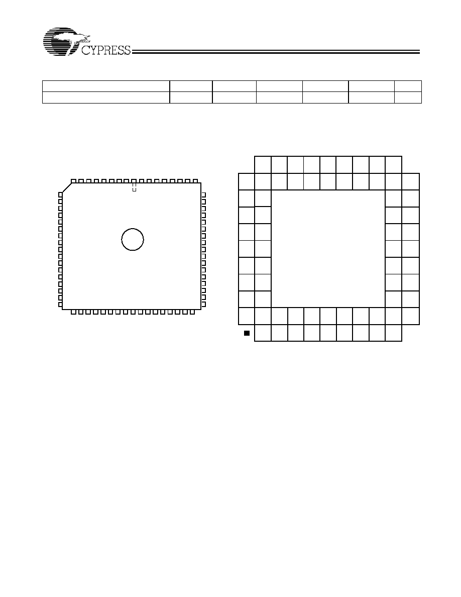
Pin Configurations
I/O
Top View
HLCC, PLCC
7 6
4
5
3
11
12
10
9 8
43
42
44
45
46
21
22
24
23
25
13
14
41
40
2
1
26 27
18
19
17
16
15
20
28 29
31
30
32 33
36
35
37 38 39
34
52
51
49
50
48
47
V
CC
53
54
55
60
58
59
57
56
66 65
63
64
62
68 67
61
I/O
INPUT
INPUT/CLK
INPUT
GND
INPUT
I/O
I/O
I/O
I/O
I/O
I/O
I/O
I/O
I/O
I/O
I/O
I/O
I/O
I/O
I/O
I/O
I/O
I/O
I/O
GND
I/O
I/O
I/O
I/O
I/O
I/O
V
CC
V
CC
INPUT
INPUT
GND
INPUT
I/O
I/O
I/O
I/O
I/O
I/O
I/O
I/O
I/O
INPUT
I/O
I/O
I/O
I/O
I/O
I/O
I/O
I/O
I/O
I/O
I/O
GND
I/O
I/O
I/O
I/O
I/O
I/O
V
CC
I/O
I/O
I/O
I/O
I/O
V
CC
I/O
INPUT/
CLK
INPUT
GND
I/O
I/O
I/O
I/O
V
CC
I/O
I/O
I/O
GND
I/O
I/O
I/O
I/O
I/O
I/O
I/O
I/O
I/O
I/O
I/O
I/O
V
CC
INPUT
INPUT
GND
INPUT
I/O
INPUT
I/O
I/O
I/O
I/O
I/O
I/O
I/O
I/O
V
CC
I/O
I/O
I/O
GND
I/O
I/O
I/O
I/O
I/O
I/O
I/O
PGA
Bottom View
I/O
INPUT INPUT
I/O
I/O
I/O
I/O
I/O
I/O
L
K
J
H
G
F
E
D
C
B
A
1
2
3
4
5
6
7
8
9
10
11
7C342B
7C342B
CY7C342B
USE ULTRA37000
TM
FOR
ALL NEW DESIGNS
Document #: 38-03014 Rev. *B
Page 3 of 14
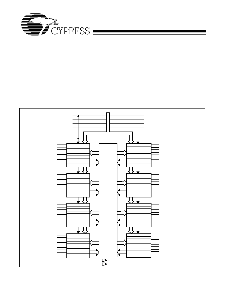
Logic Array Blocks
There are eight logic array blocks in the CY7C342B. Each LAB
consists of a macrocell array containing 16 macrocells, an
expander product term array containing 32 expanders, and an
I/O block. The LAB is fed by the programmable interconnect
array and the dedicated input bus. All macrocell feedbacks go
to the macrocell array, the expander array, and the program-
mable interconnect array. Expanders feed themselves and the
macrocell array. All I/O feedbacks go to the programmable
interconnect array so that they may be accessed by macro-
cells in other LABs as well as the macrocells in the LAB in
which they are situated.
Externally, the CY7C342B provides eight dedicated inputs,
one of which may be used as a system clock. There are 52 I/O
pins that may be individually configured for input, output, or
bidirectional data flow.
Programmable Interconnect Array
The Programmable Interconnect Array (PIA) solves inter-
connect limitations by routing only the signals needed by each
logic array block. The inputs to the PIA are the outputs of every
macrocell within the device and the I/O pin feedback of every
pin on the device.
Unlike masked or programmable gate arrays, which induce
variable delay dependent on routing, the PIA has a fixed delay.
This eliminates undesired skews among logic signals that may
cause glitches in internal or external logic. The fixed delay,
regardless of programmable interconnect array configuration,
simplifies design by assuring that internal signal skews or
races are avoided. The result is ease of design implemen-
tation, often in a signal pass, without the multiple internal logic
placement and routing iterations required for a programmable
gate array to achieve design timing objectives.
Timing Delays
Timing delays within the CY7C342B may be easily determined
using Warp
Æ
, Warp ProfessionalTM, or Warp EnterpriseTM
software by the model shown in Figure 1. The CY7C342B has
fixed internal delays, allowing the user to determine the
worst-case timing delays for any design.
Design Recommendations
Operation of the devices described herein with conditions
above those listed under "Maximum Ratings" may cause
permanent damage to the device. This is a stress rating only
and functional operation of the device at these or any other
conditions above those indicated in the operational sections of
this datasheet is not implied. Exposure to absolute maximum
ratings conditions for extended periods of time may affect
device reliability. The CY7C342B contains circuitry to protect
device pins from high static voltages or electric fields, but
normal precautions should be taken to avoid application of any
voltage higher than the maximum rated voltages.
For proper operation, input and output pins must be
constrained to the range GND < (V
IN
or V
OUT
) < V
CC
. Unused
inputs must always be tied to an appropriate logic level
(either V
CC
or GND). Each set of V
CC
and GND pins must
be connected together directly at the device. Power supply
decoupling capacitors of at least 0.2
µ
F must be connected
between V
CC
and GND. For the most effective decoupling,
each V
CC
pin should be separately decoupled to GND
directly at the device. Decoupling capacitors should have
good frequency response, such as monolithic ceramic types
have.
LOGIC ARRAY
CONTROL DELAY
t
LAC
EXPANDER
DELAY
t
EXP
CLOCK
DELAY
t
IC
t
RD
t
COMB
t
LATCH
INPUT
DELAY
t
IN
REGISTER
OUTPUT
DELAY
t
OD
t
XZ
t
ZX
LOGIC ARRAY
DELAY
t
LAD
FEEDBACK
DELAY
t
FD
OUTPUT
INPUT
SYSTEM CLOCK DELAY t
ICS
t
RH
t
RSU
t
PRE
t
CLR
PIA
DELAY
t
PIA
I/O DELAY
t
IO
Figure 1. CY7C342B Internal Timing Model
CY7C342B
USE ULTRA37000
TM
FOR
ALL NEW DESIGNS
Document #: 38-03014 Rev. *B
Page 4 of 14
Design Security
The CY7C342B contains a programmable design security
feature that controls the access to the data programmed into
the device. If this programmable feature is used, a proprietary
design implemented in the device cannot be copied or
retrieved. This enables a high level of design control to be
obtained since programmed data within EPROM cells is
invisible. The bit that controls this function, along with all other
program data, may be reset simply by erasing the entire
device.
The CY7C342B is fully functionally tested and guaranteed
through complete testing of each programmable EPROM bit
and all internal logic elements thus ensuring 100%
programming yield.
The erasable nature of these devices allows test programs to
be used and erased during early stages of the production flow.
The devices also contain on-board logic test circuitry to allow
verification of function and AC specification once encapsu-
lated in non-windowed packages.
Timing Considerations
Unless otherwise stated, propagation delays do not include
expanders. When using expanders, add the maximum
expander delay t
EXP
to the overall delay. Similarly, there is an
additional t
PIA
delay for an input from an I/O pin when
compared to a signal from straight input pin.
When calculating synchronous frequencies, use t
SU
if all
inputs are on dedicated input pins. When expander logic is
used in the data path, add the appropriate maximum expander
delay, t
EXP
to t
S1
. Determine which of 1/(t
WH
+ t
WL
), 1/t
CO1
,
or 1/(t
EXP
+ t
S1
) is the lowest frequency. The lowest of these
frequencies is the maximum data path frequency for the
synchronous configuration.
When calculating external asynchronous frequencies, use
t
AS1
if all inputs are on the dedicated input pins.
When expander logic is used in the data path, add the appro-
priate maximum expander delay, t
EXP
to t
AS1
. Determine
which of 1/(t
AWH
+ t
AWL
), 1/t
ACO1
, or 1/(t
EXP
+ t
AS1
) is the
lowest frequency. The lowest of these frequencies is the
maximum data path frequency for the asynchronous config-
uration.
The parameter t
OH
indicates the system compatibility of this
device when driving other synchronous logic with positive
input hold times, which is controlled by the same
synchronous clock. If t
OH
is greater than the minimum
required input hold time of the subsequent synchronous
logic, then the devices are guaranteed to function properly
with a common synchronous clock under worst-case
environmental and supply voltage conditions.
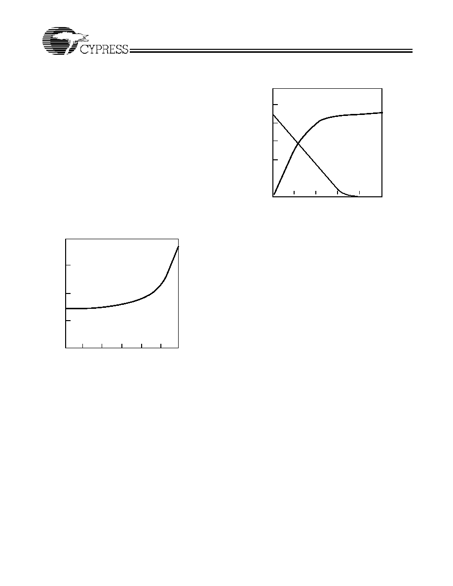
Typical I
CC
vs. f
MAX
400
300
200
100
1 kHz
10 kHz
100 kHz 1 MHz
I
CC
MAXIMUM FREQUENCY
10 MHz
0
50 MHz
100 Hz
ACTIVE (mA
)
T
y
p.
V
CC
= 5.0V
Room Temp.
Output Drive Current
0
1
2
3
4
I OU
TPUT
CURR
EN
T (
m
A)
TYPICAL
V
O
OUTPUT VOLTAGE (V)
250
200
150
100
50
5
O
I
OH
I
OL
V
CC
= 5.0V
Room Temp.
CY7C342B
USE ULTRA37000
TM
FOR
ALL NEW DESIGNS
Document #: 38-03014 Rev. *B
Page 5 of 14
Maximum Ratings
(Above which the useful life may be impaired. For user guide-
lines, not tested.)
Storage Temperature ................................ ≠65
∞
C to +135
∞
C
Ambient Temperature with
Power Applied............................................ ≠65
∞
C to +135
∞
C
Maximum Junction Temperature
(under bias)..................................................................150
∞
C
Supply Voltage to Ground Potential ............≠2.0V to +7.0V
[1]
DC Output Current per Pin
[1]
................... ≠25 mA to +25 mA
DC Input Voltage
[1]
.........................................≠2.0V to +7.0V
Operating Range
Range
Ambient Temperature
V
CC
Commercial
0
∞
C to +70
∞
C
5V
±
5%
Industrial
≠40
∞
C to +85
∞
C
5V
±
10%
Electrical Characteristics
Over the Operating Range
Parameter
Description
Test Conditions
Min.
Max.
Unit
V
CC
Supply Voltage
Maximum V
CC
rise time is 10 ms
4.75(4.5)
5.25(5.5)
V
V
OH
Output HIGH Voltage
I
OH
= ≠4 mA DC
[2]
2.4
V
V
OL
Output LOW Voltage
I
OL
= 8 mA DC
[2]
0.45
V
V
IH
Input HIGH Voltage
2.0
V
CC
+ 0.3
V
V
IL
Input LOW Voltage
≠0.3
0.8
V
I
IX
Input Current
V
I
= V
CC
or ground
≠10
+10
µ
A
I
OZ
Output Leakage Current
V
O
= V
CC
or ground
≠40
+40
µ
A
t
R
Recommended Input Rise Time
100
ns
t
F
Recommended Input Fall Time
100
ns
Capacitance
Parameter
Description
Test Conditions
Max.
Unit
C
IN
Input Capacitance
V
IN
= 0V, f = 1.0 MHz
10
pF
C
OUT
Output Capacitance
V
OUT
= 0V, f = 1.0 MHz
20
pF
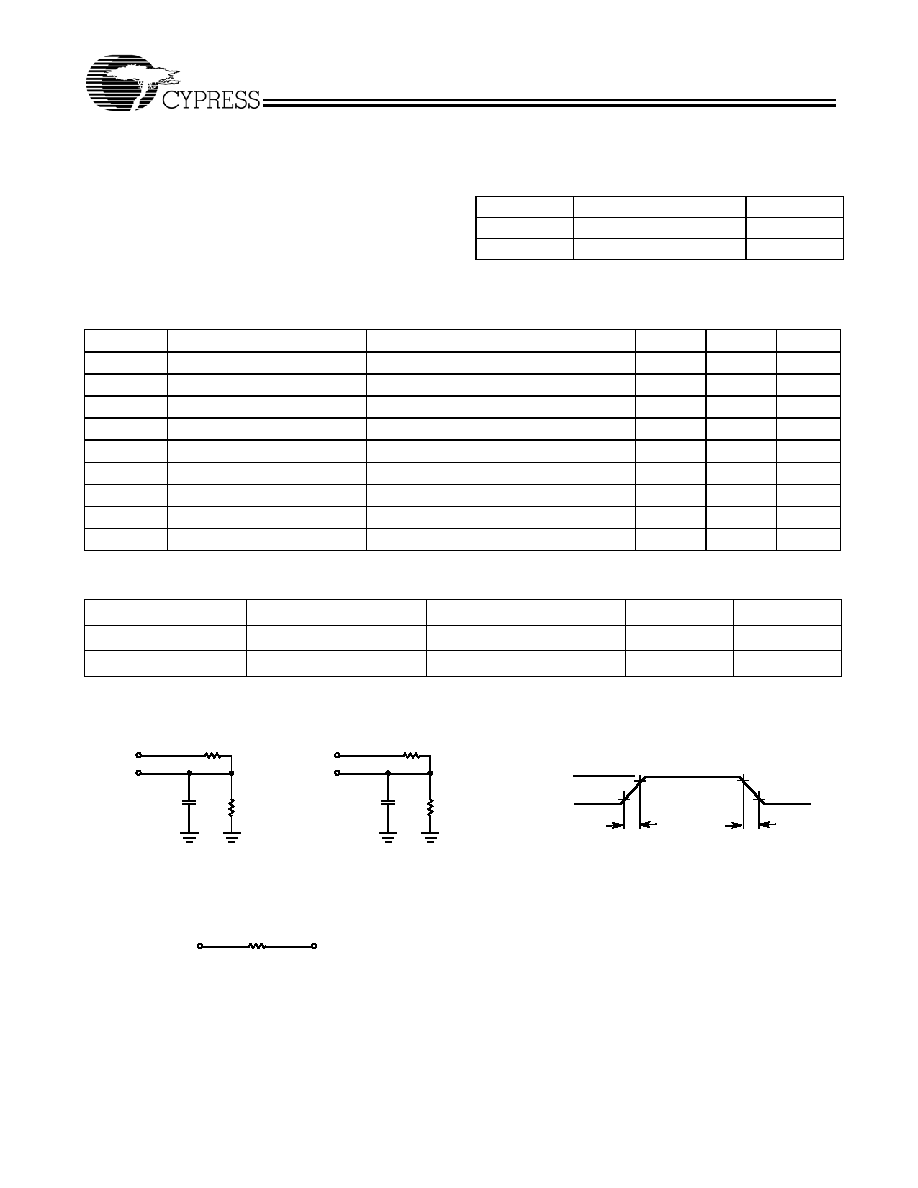
AC Test Loads and Waveforms
Notes:
1. Minimum DC input is ≠0.3V. During transactions, input may undershoot to ≠2.0V or overshoot to 7.0V for input currents less then 100 mA and periods shorter
than 20 ns.
2. The I
OH
parameter refers to high-level TTL output current; the I
OL
parameter refers to low-level TTL output current.
3.0V
5V
OUTPUT
R1 464
R2
250
50 pF
INCLUDING
JIG AND
SCOPE
GND
90%
10%
90%
10%
6 ns
6 ns
5V
OUTPUT
R1 464
R2
250
5 pF
INCLUDING
JIG AND
SCOPE
(a)
(b)
OUTPUT
1.75V
Equivalent to:
TH… VENIN EQUIVALENT (commercial/military)
ALL INPUT PULSES
163