Untitled Document
32-Macrocell MAX® EPLD
CY7C344B
Cypress Semiconductor Corporation
·
3901 North First Street
·
San Jose
·
CA 95134
·
408-943-2600
Document #: 38-03036 Rev. **
Revised December 8, 1999
44B
Features
· High-performance, high-density replacement for TTL,
74HC, and custom logic
· 32 macrocells, 64 expander product terms in one LAB
· 8 dedicated inputs, 16 I/O pins
· Advanced 0.65-micron CMOS EPROM technology to
increase performance
· 28-pin, 300-mil DIP, cerDIP or 28-pin HLCC, PLCC
package
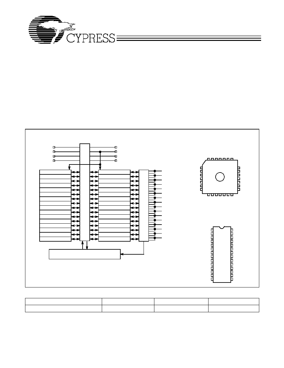
Functional Description
Available in a 28-pin, 300-mil DIP or windowed J-leaded ce-
ramic chip carrier (HLCC), the CY7C344B represents the
densest EPLD of this size. Eight dedicated inputs and 16 bidi-
rectional I/O pins communicate to one logic array block. In the
CY7C344B LAB there are 32 macrocells and 64 expander
product terms. When an I/O macrocell is used as an input, two
expanders are used to create an input path. Even if all of the
I/O pins are driven by macrocell registers, there are still 16
"buried" registers available. All inputs, macrocells, and I/O pins
are interconnected within the LAB.
The speed and density of the CY7C344B makes it a natural for
all types of applications. With just this one device, the designer
can implement complex state machines, registered logic, and
combinatorial "glue" logic, without using multiple chips. This
architectural flexibility allows the CY7C344B to replace multi-
chip TTL solutions, whether they are synchronous, asynchro-
nous, combinatorial, or all three.
MAX is a registered trademark of Altera Corporation.
C344B1
Logic Block Diagram
MACROCELL 2
MACROCELL 4
MACROCELL 6
MACROCELL 8
MACROCELL 10
MACROCELL 12
MACROCELL 14
MACROCELL 16
MACROCELL 18
MACROCELL 20
MACROCELL 22
MACROCELL 24
MACROCELL 26
MACROCELL 28
MACROCELL 30
MACROCELL 32
MACROCELL 1
MACROCELL 3
MACROCELL 5
MACROCELL 7
MACROCELL 9
MACROCELL 11
MACROCELL 13
MACROCELL 15
MACROCELL 17
MACROCELL 19
MACROCELL 21
MACROCELL 23
MACROCELL 25
MACROCELL 27
MACROCELL 29
MACROCELL 31
G
L
O
B
A
L
B
U
S
I
O
C
O
N
T
R
O
L
INPUT
INPUT
INPUT
INPUT
15(22)
15(23)
27(6)
28(7)
INPUT
1(8)
INPUT/CLK
2(9)
INPUT
13(20)
INPUT
14(21)
I/O
3(10)
I/O
4(11)
I/O
5(12)
I/O
6(13)
I/O
9(16)
I/O
10(17)
I/O
11(18)
I/O
12(19)
I/O
17(24)
I/O
18(25)
I/O
19(26)
I/O
20(27)
I/O
23(2)
I/O
24(3)
I/O
25(4)
I/O
26(5)
64 EXPANDER PRODUCT TERM ARRAY
32
Pin Configurations
Top View
HLCC
25
24
23
22
21
20
19
5
6
7
8
9
10
11
12 13 14 1516 1718
4 3 2
28 27 26
I/O
I/O
INPUT
INPUT
INPUT
I/O
I/O
INPUT
INPUT
INPUT/CLK
I/O
I/O
I/O
I/O
I/O
GND
I/O
I/O
I/O
I/O
V CC
1
V
CC
INPUT
C344B2
I/O
GND
I/O
I/O
INPUT
1
2
3
4
5
6
7
8
9
10
11
12
13
14
28
27
26
25
24
23
22
21
20
19
18
17
16
15
INPUT
INPUT
Top View
CerDIP
INPUT/CLK
I/O
I/O
I/O
I/O
V
CC
GND
I/O
I/O
I/O
I/O
INPUT
INPUT
INPUT
I/O
I/O
I/O
I/O
V
CC
GND
I/O
I/O
I/O
I/O
INPUT
INPUT
C344B3
[1]
Selection Guide
7C344B-15
7C344B-20
7C344B-25
Maximum Access Time (ns)
15
20
25
Note:
1.
Number in () refers to J-leaded packages.
CY7C344B
Document #: 38-03036 Rev. **
Page 2 of 12
Maximum Ratings
(Above which the useful life may be impaired. For user guide-
lines, not tested.)
Storage Temperature ................................. 65
°
C to +135
°
C
Ambient Temperature with
Power Applied..............................................-65
°
C to +135
°
C
Maximum Junction Temperature (Under Bias)............. 150
°
C
Supply Voltage to Ground Potential
[2]
............ 2.0V to +7.0V
DC Output Current, per Pin
[2]
...................25 mA to +25 mA
DC Input Voltage
[2]
.........................................2.0V to +7.0V
Operating Range
Range
Ambient
Temperature
V
CC
Commercial
0
°
C to +70
°
C
5V
±
5%
Industrial
40
°
C to +85
°
C
5V
±
10%
Electrical Characteristics
Over the Operating Range
Parameter
Description
Test Conditions
Min.
Max.
Unit
V
CC
Supply Voltage
Maximum V
CC
rise time is 10 ms
4.75(4.5)
5.25(5.5)
V
V
OH
Output HIGH Voltage
I
OH
= 4.0 mA DC
[3]
2.4
V
V
OL
Output LOW Voltage
I
OL
= 8 mA DC
[3]
0.45
V
V
IH
Input HIGH Level
2.0
V
CC
+0.3
V
V
IL
Input LOW Level
0.3
0.8
V
I
IX
Input Current
GND
V
IN
V
CC
10
+10
µ
A
I
OZ
Output Leakage Current
V
O
= V
CC
or GND
40
+40
µ
A
t
R
Recommended Input Rise Time
100
ns
t
F
Recommended Input Fall Time
100
ns
Capacitance
Parameter
Description
Test Conditions
Max.
Unit
C
IN
Input Capacitance
V
IN
= 0V, f = 1.0 MHz
10
pF
C
OUT
Output Capacitance
V
OUT
= 0V, f = 1.0 MHz
12
pF
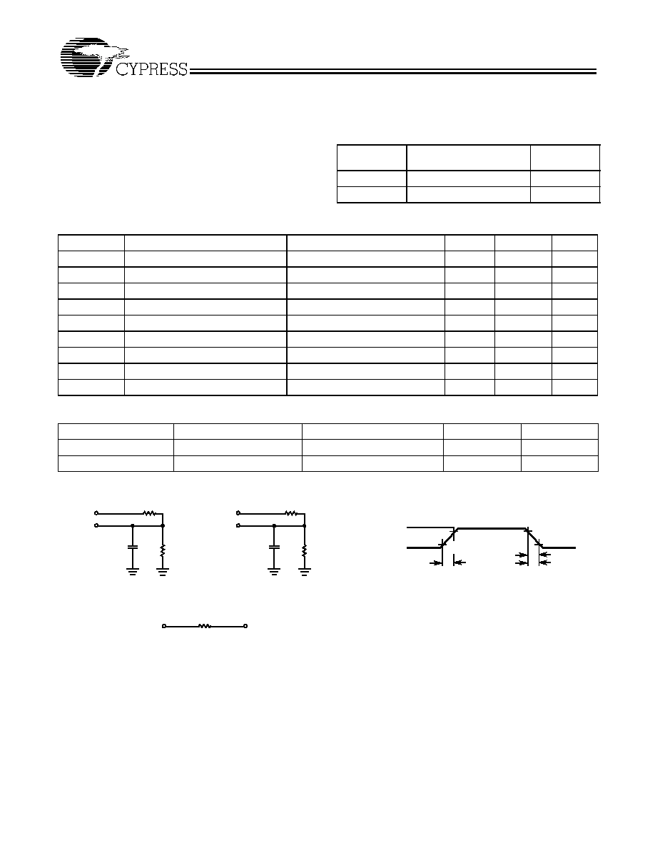
AC Test Loads and Waveforms
Notes:
2.
Minimum DC input is 0.3V. During transactions, the inputs may undershoot to 2.0V or overshoot to 7.0V for input currents less then 100 mA and periods
shorter than 20 ns.
3.
The I
OH
parameter refers to high-level TTL output current; the I
OL
parameter refers to low-level TTL output current.
3.0V
5V
OUTPUT
R1 464
R2
250
50 pF
INCLUDING
JIGAND
SCOPE
GND
90%
10%
90%
10%
6 ns
6 ns
5V
OUTPUT
R1 464
R2
250
(a)
(b)
OUTPUT
1.75V
Equivalent to:
THÉVENIN EQUIVALENT (commercial)
C344B5
C344B6
ALL INPUT PULSES
t
f
5 pF
C344B7
t
R
t
F
163
CY7C344B
Document #: 38-03036 Rev. **
Page 3 of 12
Design Recommendations
Operation of the devices described herein with conditions
above those listed under "Absolute Maximum Ratings" may
cause permanent damage to the device. This is a stress rating
only and functional operation of the device at these or any
other conditions above those indicated in the operational sec-
tions of this data sheet is not implied. Exposure to absolute
maximum ratings conditions for extended periods of time may
affect device reliability. The CY7C344B contains circuitry to
protect device pins from high-static voltages or electric fields;
however, normal precautions should be taken to avoid apply-
ing any voltage higher than maximum rated voltages.
For proper operation, input and output pins must be con-
strained to the range GND
(V
IN
or V
OUT
)
V
CC
. Unused
inputs must always be tied to an appropriate logic level (either
V
CC
or GND). Each set of V
CC
and GND pins must be connect-
ed together directly at the device. Power supply decoupling
capacitors of at least 0.2
µ
F must be connected between V
CC
and GND. For the most effective decoupling, each V
CC
pin
should be separately decoupled.
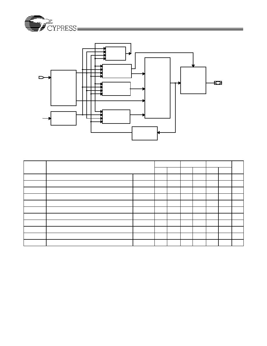
Timing Considerations
Unless otherwise stated, propagation delays do not include
expanders. When using expanders, add the maximum ex-
pander delay t
EXP
to the overall delay.
When calculating synchronous frequencies, use t
SU
if all in-
puts are on the input pins. When expander logic is used in the
data path, add the appropriate maximum expander delay, t
EXP
to t
SU
. Determine which of 1/(t
WH
+ t
WL
), 1/t
CO1
, or 1/(t
EXP
+
t
SU
) is the lowest frequency. The lowest of these frequencies
is the maximum data-path frequency for the synchronous con-
figuration.
When calculating external asynchronous frequencies, use
t
AS1
if all inputs are on dedicated input pins.
When expander logic is used in the data path, add the appro-
priate maximum expander delay, t
EXP
to t
AS1
. Determine which
of 1/(t
AWH
+ t
AWL
), 1/t
ACO1
, or 1/(t
EXP
+ t
AS1
) is the lowest
frequency. The lowest of these frequencies is the maximum
data-path frequency for the asynchronous configuration.
The parameter t
OH
indicates the system compatibility of this
device when driving other synchronous logic with positive in-
put hold times, which is controlled by the same synchronous
clock. If t
OH
is greater than the minimum required input hold
time of the subsequent synchronous logic, then the devices
are guaranteed to function properly with a common synchro-
nous clock under worst-case environmental and supply volt-
age conditions.
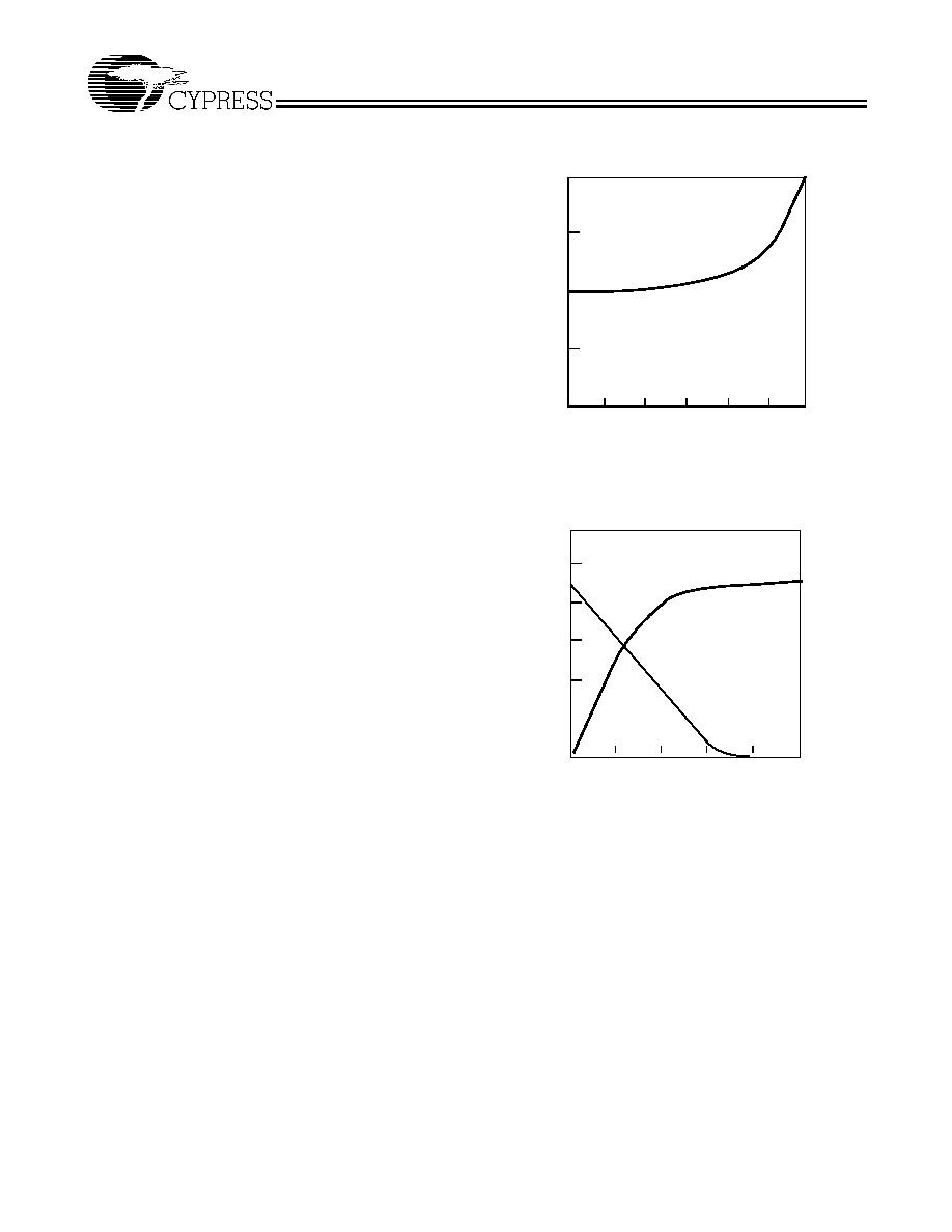
Typical I
CC
vs. f
MAX
Output Drive Current
240
180
120
60
1 kHz
10 kHz
100 kHz
1 MHz
I
CC
MAXIMUM FREQUENCY
10 MHz
0
50 MHz
100 Hz
ACT
I
V
E
(mA
) T
y
p.
V
CC
=5.0V
Room Temp.
C344B8
0
1
2
3
4
I
OUT
P
UT CUR
RE
NT (
m
A
)
TY
P
I
C
A
L
V
O
OUTPUT VOLTAGE (V)
250
200
150
100
50
5
O
I
OH
I
OL
V
CC
=5.0V
Room Temp.
C344B9
CY7C344B
Document #: 38-03036 Rev. **
Page 4 of 12
Figure 1. CY7C344B Timing Model
LOGIC ARRAY
CONTROLDELAY
t
LAC
EXPANDER
DELAY
t
EXP
CLOCK
DELAY
t
IC
t
RD
t
COMB
t
LATCH
INPUT
DELAY
t
IN
REGISTER
OUTPUT
DELAY
t
OD
t
XZ
t
ZX
LOGIC ARRAY
DELAY
t
LAD
FEEDBACK
DELAY
t
FD
OUTPUT
INPUT
C344B10
SYSTEM CLOCK DELAYt
ICS
t
RH
t
RSU
t
PRE
t
CLR
I/O
I/O DELAY
t
IO
I/O
External Synchronous Switching Characteristics
Over Operating Range
7C344B-15
7C344B-20
7C344B-25
Parameter
Description
Min.
Max.
Min.
Max.
Min.
Max.
Unit
t
PD1
Dedicated Input to Combinatorial Output Delay
[4]
Com'l/Ind
15
20
25
ns
t
PD2
I/O Input to Combinatorial Output Delay
[4]
Com'l/Ind
15
20
25
ns
t
SU
Global Clock Set-up Time
Com'l/Ind
9
12
15
ns
t
CO1
Synchronous Clock Input to Output Delay
[4]
Com'l/Ind
10
12
15
ns
t
H
Input Hold Time from Synchronous Clock Input
Com'l/Ind
0
0
0
ns
t
WH
Synchronous Clock Input HIGH Time
Com'l/Ind
6
7
8
ns
t
WL
Synchronous Clock Input LOW Time
Com'l/Ind
6
7
8
ns
f
MAX
Maximum Register Toggle Frequency
[5]
Com'l/Ind
83.3
71.4
62.5
MHz
t
CNT
Minimum Global Clock Period
Com'l/Ind
13
16
20
ns
t
ODH
Output Data Hold Time After Clock
Com'l/Ind
1
1
1
ns
f
CNT
Maximum Internal Global Clock Frequency
[6]
Com'l/Ind
76.9
62.5
50
MHz
Notes:
4.
C1 = 35 pF
5.
The f
MAX
values represent the highest frequency for pipeline data.
6.
This parameter is measured with a 32-bit counter programmed into each LAB.
CY7C344B
Document #: 38-03036 Rev. **
Page 5 of 12
External Asynchronous Switching Characteristics
Over Operating Range
7C344B-15
7C344B-20
7C344B-25
Parameter
Description
Min.
Max.
Min.
Max.
Min.
Max.
Unit
t
ACO1
Asynchronous Clock Input to Output Delay
[4]
Com'l/Ind
15
18
22
ns
t
AS1
Dedicated Input or Feedback Set-Up Time to
Asynchronous Clock Input
Com'l/Ind
5
6
8
ns
t
AH
Input Hold Time from Asynchronous Clock Input
Com'l/Ind
5
6
8
ns
t
AWH
Asynchronous Clock Input HIGH Time
[7]
Com'l/Ind
6
7
9
ns
t
AWL
Asynchronous Clock Input LOW Time
[7]
Com'l/Ind
7
9
11
ns
t
ACNT
Minimum Internal Array Clock Frequency
Com'l/Ind
13
16
20
ns
f
ACNT
Maximum Internal Array Clock Frequency
[6]
Com'l/Ind
76.9
62.5
50
MHz
Typical Internal Switching Characteristics
Over Operating Range
7C344B-15
7C344B-20
7C344B-25
Parameter
Description
Min.
Max.
Min.
Max.
Min.
Max.
Unit
t
IN
Dedicated Input Pad and Buffer Delay
Com'l/Ind
3
5
7
ns
t
IO
I/O Input Pad and Buffer Delay
Com'l/Ind
3
5
7
ns
t
EXP
Expander Array Delay
Com'l/Ind
8
10
15
ns
t
LAD
Logic Array Data Delay
Com'l/Ind
7
10
13
ns
t
LAC
Logic Array Control Delay
Com'l/Ind
4
4
4
ns
t
OD
Output Buffer and Pad Delay
[4]
Com'l/Ind
4
4
4
ns
t
ZX
Output Buffer Enable Delay
[4]
Com'l /Ind
7
7
7
ns
t
XZ
Output Buffer Disable Delay
[4]
Com'l/Ind
7
7
7
ns
t
RSU
Register Set-Up Time Relative to Clock Signal
at Register
Com'l/Ind
4
4
5
ns
t
RH
Register Hold Time Relative to Clock Signal at
Register
Com'l/Ind
5
8
10
ns
t
LATCH
Flow-Through Latch Delay
Com'l/Ind
1
1
1
ns
t
RD
Register Delay
Com'l/Ind
1
1
1
ns
t
COMB
Transparent Mode Delay
Com'l/Ind
1
1
1
ns
t
IC
Asynchronous Clock Logic Delay
Com'l/Ind
7
8
10
ns
t
ICS
Synchronous Clock Delay
Com'l/Ind
2
2
3
ns
t
FD
Feedback Delay
Com'l/Ind
1
1
1
ns
t
PRE
Asynchronous Register Preset Time
Com'l/Ind
5
6
9
ns
t
CLR
Asynchronous Register Clear Time
Com'l/Ind
5
6
9
ns
Notes:
7.
This parameter is measured with a positive-edge-triggered clock at the register. For the negative-edge clocking, the t
ACH
and t
ACL
parameter must be swapped.